Functionalized pentacene field-effect transistors with logic circuit applications
Abstract
Funtionalized pentacene, 6,13-bis(triisopropylsilylethynyl)pentacene (TIPS-pentacene), field-effect transistors(FET’s) were made by thermal evaporation or solution deposition method and the mobility was measured as a function of temperature and light power. The field-effect mobility (FET) has a gate-voltage dependent activation energy. A non-monotonic temperature dependence was observed at high gate voltage (VG -30 V) with activation energy Ea 60 - 170 meV,depending on the fabrication procedure. The gate-voltage dependent mobility and non-monotonic temperature dependence indicates that shallow traps play important role in the transport of TIPS-pentacene films. The current in the saturation regime as well as mobility increase upon light illumination and is proportional to the light intensity, mainly due to the photoconductive response. Transistors with submicron channel length showed unsaturating current-voltage characteristics due to the short channel effect. Realization of simple circuits such as NOT(inverter), NOR, and NAND logic gates are demonstrated for thin film TIPS-pentacene transistors.
I Introduction
The use of organic material for the electronic devices has great importance for future application due to its low cost and easy fabrication procedures. Pentacene, one of most promising organic material for device application, has been studied intensively in polycrystallineJackson or single crystalline structuresRamirez due to its high room temperature hole mobility more than 1 cm2/Vs. And other polyacene single crystals such as tetraceneMorpurgo , anthracenePark as well as thin film structuresJackson_tet were also investigated.
By attaching the side functional group, soluble and stable functionalized pentacene can be madeAnthony and this make its fabrication methods versitile and increase application for devices. Transport measurement depending on its crystal directionBrooks1 shows different conducting properties and the persistent photoconductivity was already reported.Brooks2 Field-effect transistor (FET) application of these functionalized pentacene was shownJackson2 ; Payne and they can get room temperature mobility up to 0.4 cm2/Vs with deposition under substrate heating and gate dielectric with self-assembled monolayer. Temperature dependence of mobility is key to elucidate its quality and transport mechanism. In the case of field-effect mobility, band-like temperature dependence is very rare and only observed at high temperature range in single crystalMorpurgo ; Park and thin filmJackson3 .
In addition to the electrical applications, its photosensitive propertiesBrooks2 can be used as light detector or optical switch. Light responsive properties of organic transistor have not been investigated as much as electrical properties. The performance of photoresponsivity in polymerKumar ; Noh and pentaceneLiang is still lower than that of amorphous silicon ( 300 A/W). However, this can be improved by optimization of device fabrication
In this article, we report the electrical and optical properties of 6,13-bis(triisopropylsilylethynyl)pentacene (TIPS-pentacene) FET. For the electrical properties, we measured field-effect mobility of thin film or single crystal transistor. In temperature dependence, field-effect mobility exhibit gate voltage dependent activation energy and it shows nonmonotonous temperature dependence at Vg -30 V region. This was also observed irrespective of fabrication method. At nanoscale electrodes we cannot observe current saturation as in the case of micron scale FET. The light illumination above absorption edge of TIPS-pentacene enhanced the saturation current of transistor more than 4 orders of magnitude and slightly increased its mobility. By adding off-chip resistor to thin film transistor, we realized logic circuits such as NOT, NAND, and NOR at room temperature.
II Experiment
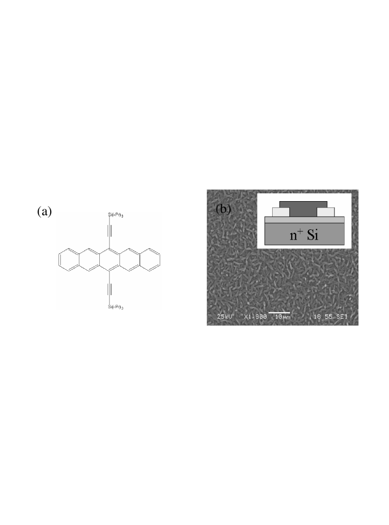
TIPS-pentacene (Fig. 1 (a)) was synthesized as described in elsewhereAnthony and it was thermally evaporated with ( 70 ∘C) or without substrate heating at base pressure less than 5 10 -6 Torr. After drying of 2 wt. % toluene solution droplet, single crystalline films are formed on the surface. Predefined microelectrodes from photolithography with channel length (L) of 5 m 40 m and channel width (W) of 400m 6 cm were used for source and drain contacts and heavily doped n-type Si substrate( 0.002 cm) served as a back gate. Thermally grown 300 nm SiO2 layer used for gate dielectric without molecular modification. For the nanoelectrodes fabrication, we used e-beam lithography and lift-off process. Electrodes with 200 nm channel length and 2 m channel width were used for nanochannel FET. The thickness of TIPS-pentacene is 50 nm to 800 nm and all the devices are bottom contact configuration.
Figure 1 (b) is typical scanning electron microscope (SEM) image of evaporated TIPS-pentacene film. Its X-ray diffraction data (not shown) shows clear c-axis orientation as evaporated pentacene film. Electrical characterization is performed using HP 4155C semiconductor parameter analyzer.
III Results and discussion
III.1 Thin film and single crystalline transistor
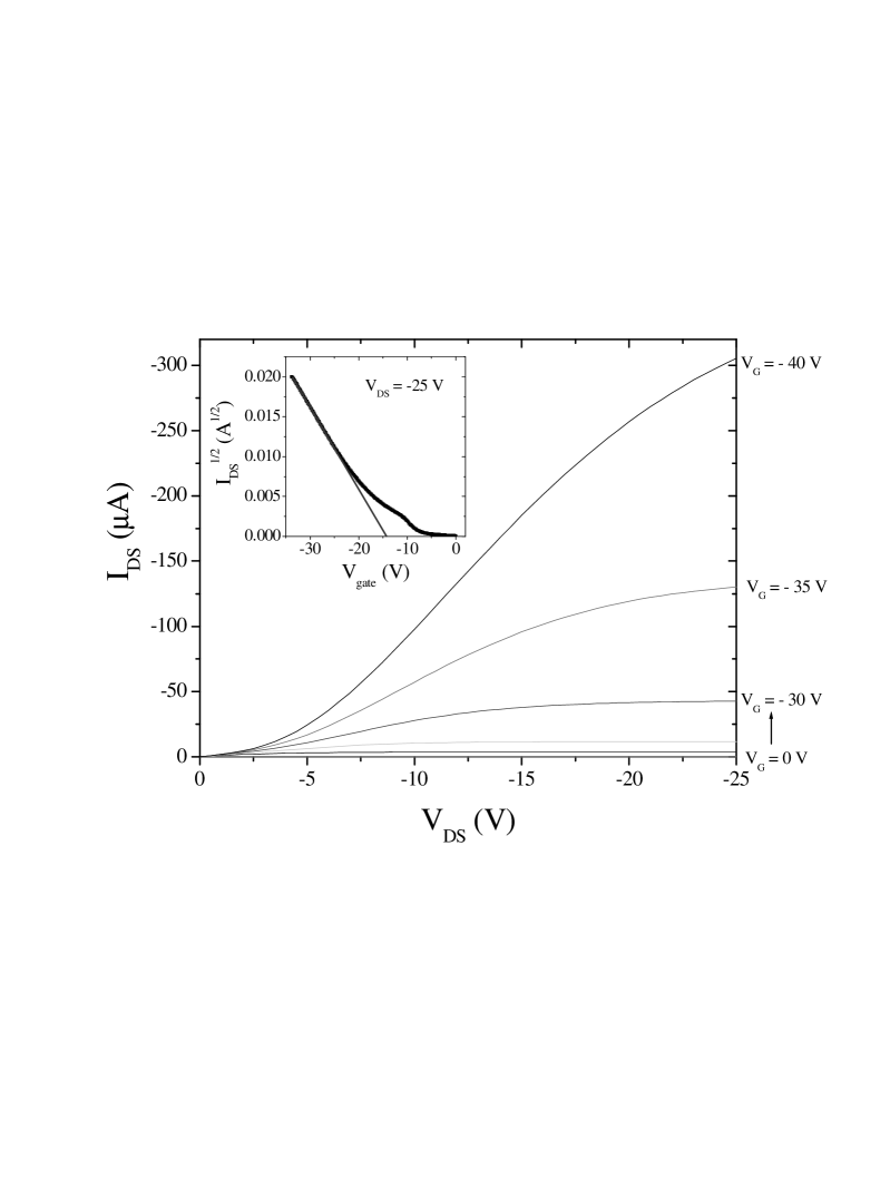
Figure 2 is typical output characteristics of TIPS-pentacene FET at room temperature and inset shows transfer characteristics in the saturation regime(VDS = -25 V). The gate voltage, Vg, was swept from 0 to -40 V in both cases. This device has room temperature mobility of 0.02 cm2/Vs and on/off current ratio higher than 106. The estimated subthreshold slope is 2.6 V/decade, that is comparable to the pentacene thin film and higher than some single crystal.Batlogg Without any modification of electrodes and substrate, most of the samples have room temperature mobility between 0.002 to 0.03 cm2/Vs.
The solution deposited film and evaporated thin film with substrate heating have slightly higher room temperature mobility of 0.08 cm2/Vs and 0.05 cm2/Vs and subthreshold swing of 3.8 V/decade and 2.1 V/decade respectively.
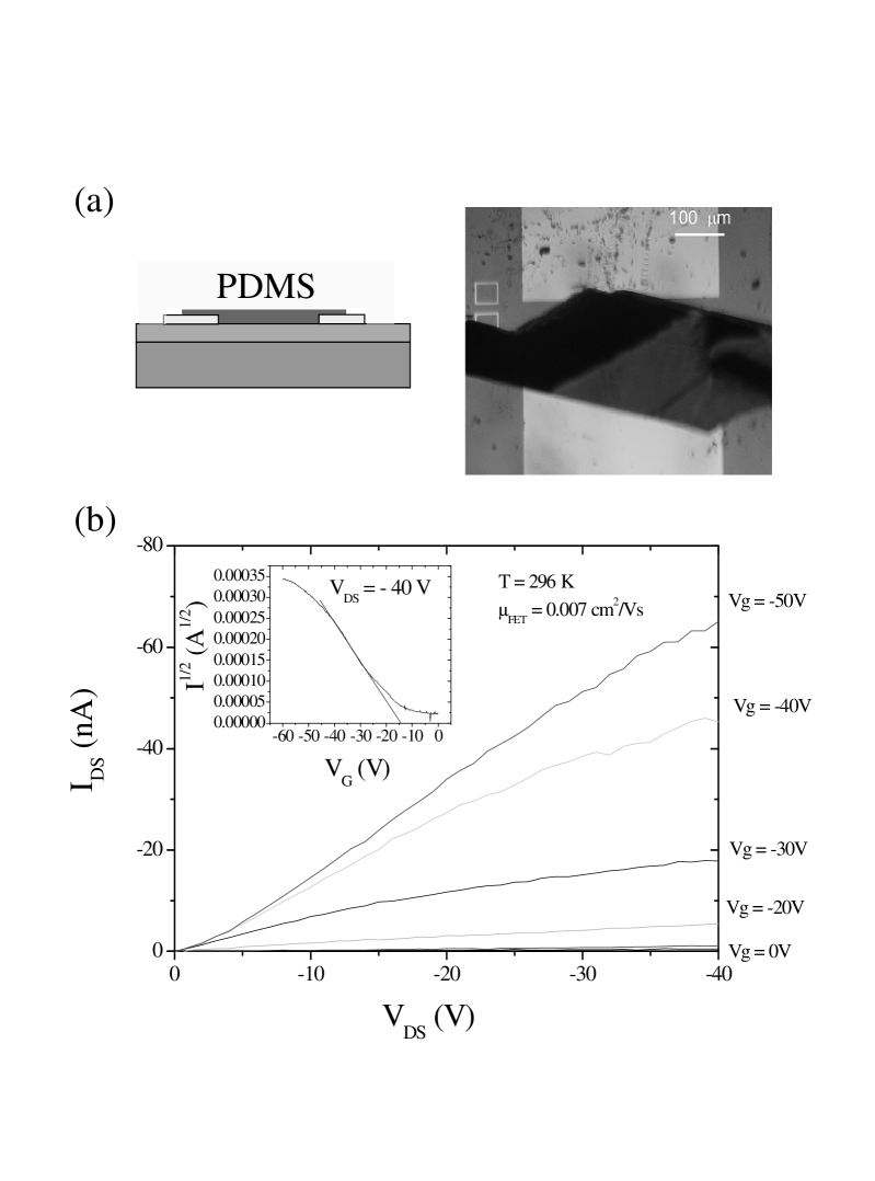
Several groups have measured single crystal FETsRamirez ; Morpurgo ; Park ; Podzorov to get intrinsic properties of organic FET. We also have used TIPS-pentacene single crystal as synthesized and put it on top of electrodes under microscope. To improve contact, transparent polydimethylsiloxane (PDMS) stamp was laid on the crystal as described in elsewherePark . The schematic diagram and its optical image was shown in Fig. 3 (a). The channel length is 100 m and effective channel width from the image is 300 m. The output characteristics (Fig. 3 (b)) also show current enhancement at negative gate voltage and transfer characteristics (VDS = - 40 V) in the inset show room temperature mobility 0.007 cm2/Vs and subthreshold swing of around 10 V/decade. Compared to the previous mentioned evaporated or solution deposited FET, the mobility is decreased and subthreshold swing is increased. A single crystal FET is very sensitive to surface status, however, from the optical microscope image the thickness of crystal is not uniform and the crystal direction is not optimized. Therefore, this can be improved in uniform and thin crystal with optimized crystal arrangement.
III.2 Temperature dependence of mobility
Figure 4 (a) shows temperature dependence of mobility at different gate voltages in evaporated film. To avoid persistent photoconductivityBrooks2 we kept the sample in dark condition for a while. At low gate voltage, mobility shows monotonous temperature dependence with exp(-/) but at high gate voltage, it reaches maximum value (T 250 K) and decreases with decrease of temperature. Unlike the gate-voltage independent mobility of tetracene or rubrene single crystalsMorpurgo ; Podzorov , mobility of TIPS-pentacene thin film is gate-voltage dependent and increase linearly upon gate voltage. This means that induced charge carrier contribute to the conduction. And trap and grain boundary are important to this activation type conduction. Inset shows the change of activation energy depending on the gate voltage. The activation energy at low gate voltage is Ea 0.27 eV, which is lower than that of bulk experiment(550 meV).Brooks2 The activation energy decreased down to 60 meV with increasing gate voltage. This kind of gate voltage dependent activation process was widely observed in thin film pentaceneBrown ; Yao , single crystalline pentaceneRamirez ; Schoonveld or oligothiopheneSchoonveld . At low temperature region (T Tm), the activation energy is 60 - 80 meV at high gate voltage (- 40 V Vg - 30 V) region.
Typical temperature dependences of FET mobility from different fabrication processes are shown in Fig. 4 (b). Generally, FETs fabricated with substrate heating or deposited from solution have higher room temperature mobility than normally deposited film. Thin film with substrate heating has activation energy, Ea = 110 - 170 meV with no mobility maximum in measured temperature range (Tm 310 K). On the other hand, activation energy of solution deposited film and thin film evaporated without substrate heating is 110 meV and 70 meV respectively. From all the temperature dependence, sample with higher Tm has high Ea, which means that trap is more dominant in this case therefore intrinsic transport is suppressed. To explain this nonmonotonous temperature dependence, several group have adopted following equationMorpurgo ; Park
| (1) |
where is the shallow trapping energy and is the Boltzmann constant.
This nonmonotonous temperature dependence can be understood that in the high temperature region, microscopic mobility would be dominant(i.e., intrinsic) and for low temperature region, thermally activated mobility would be important due to traps. This was widely observed in tetraceneMorpurgo , anthracene Park , rubrenePodzorov , and thin film pentaceneJackson3 .
The activation energy of TIPS-pentacene is larger than thermally evaporated pentacene thin film transistor (38 meV with room temperature mobility of 0.3 cm2/Vs)Jackson3 but less than precursor-route pentacene thin filmBrown .
The gate-voltage dependent mobility and nonmonotonous temperature dependence mean that shallow traps play important role in the transport of TIPS-pentacene film.
| Sample | mobility | VT | subthreshold swing | Et |
|---|---|---|---|---|
| (cm2/Vs) | (V) | (V/decade) | (meV) | |
| thin film111without substrate heating. | 0.02 | -14 | 1.9 | 70 |
| thin film222substrate heating at 70 ∘C. | 0.08 | -18 | 2.1 | 110 |
| single crystalline333solution processed. | 0.05 | -12 | 3.8 | 170 |
| single crystalline444as synthesized. | 0.007 | -15 | 10.0 | na |
III.3 Light illumination
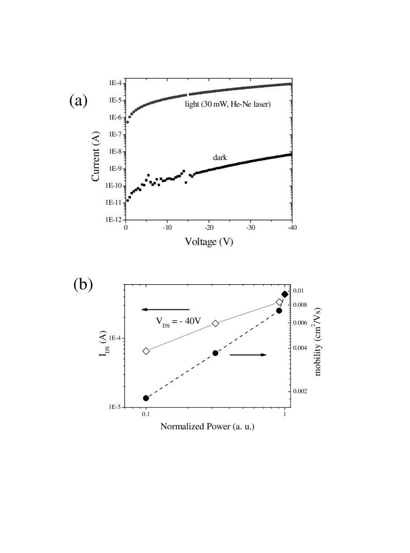
We illuminated 30 mW He-Ne laser ( = 632.8 nm) to the evaporated TIPS-pentacene FET, channel length of 5 m and channel width 6 cm. Since the absorption edge of TIPS-pentacene is around 700 nm, there is nearly 4 orders of current increase upon light illumination (Fig. 5 (a)). With (Vg= -40V) or without gate voltage, the current gain, Idlight/Id, due to light is 104. Illumination on the device generate electron-hole pairs in the channel as well as in bulk TIPS-pentancene. Current saturation indicates that it is also channel restricted as observed in photoresponsive polymer FETKumar . Estimated photoresponsivity, shown in Fig. 5 (a), is around 0.03 A/W and we can get up to 0.4 A/W in some devices.
We used filter to control optical power. As shown in Fig. 4 (b), light illumination increases the source-drain current (IDS) and mobility in proportion to optical power. Unlike semi-logarithmic response of Id vs intensity in phototransistorLakshmi , photocurrent increase with light intensity, Iph Poptα. In most photoconductive polymer films and organic materials, this exponent = 1. However, in the case of bimolecular recombination instead of monomolecular recombination, = 0.5.Lee The exponent of saturated current, Id,sat vs. optical power in Fig. 5 (b) is 0.78. When there is carrier traps, immobilized carrier cannot participate to recombination. This smaller exponent less than one means that traps play important role.
Generally, the increase of carrier density () can be estimated from = C, where Ci is the dielectric capacitance per unit area and is the shift of the threshold voltage. In this device, is around 30 V, hence can be estimated to be 1.9 1012/cm2. In the case of pentaceneLiang or GaN nanowireZhou , light illumination increase only the carrier concentration and has small effect on the mobility. TIPS-pentacene shows mobility increase by factor of 5 upon light illumination.
III.4 Nanoscale FET
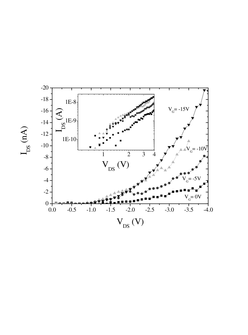
We reduced the channel length in the submicron range. The gate-dependent I-V characteristics of 200 nm channel length and 2 m channel width FET is shown in Fig. 6. TIPS-pentacene was thermally evaporated on top of electrodes that was predifined by e-beam lithography. Unlike the micron scale FET, it doesn’t show any current saturation. This is due to short channel effectSze ; Chou , that source-drain electrodes themselves make depletion, and space charge limited cunduction (SCLC) is preventing current saturation. The SCLC follows , where depends on the trap concentration and typically larger than 2. In TIPS-pentacene nanoscale FET, exponent is between 2.5 and 3 (shown in the inset of Fig. 6).
Since there is no saturation region in this device, we assume the lower voltage region to linear regime of transistor for the estimation of mobility.
| (2) |
where Ci is the gate insulator capacitance per unit area.
The estimated mobility is 0.002 cm2/Vs (at VDS = -2.5 V), that is similar to lower mobility sample in Fig. 4 (b).
III.5 Logic gate application
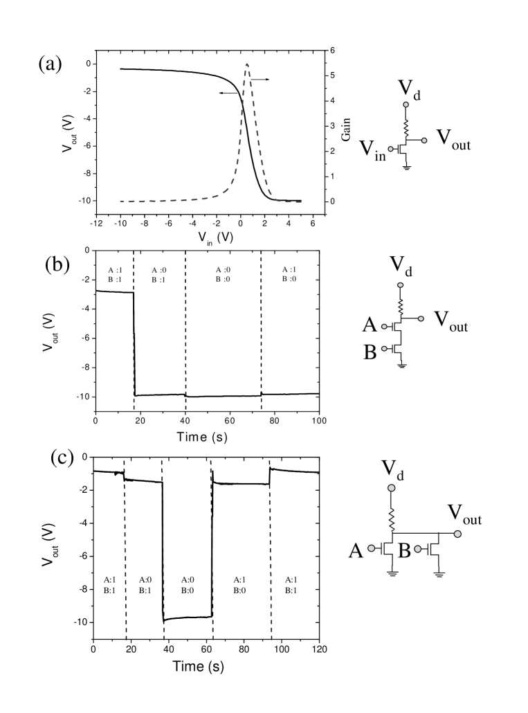
We have fabricated inverter (NOT) using this p-type TIPS-pentacene FET and off-chip resistor as shown in schematic diagram of Fig. 7 (a). A FET with room temperature mobility of 0.002 cm2/Vs (thickness of 50 nm) and serial resistor of 10 M were combined for inverter. When the input voltage is Vin 2 V (logical 0), the transistor resistance is larger than that of series resistor, therefore Vout = -10 V (logical 1). When Vin = - 10 V (logical 1), the transistor resistance is lower than that of series resistor and Vout = 0 V (logical 0). The maximum gain defined by dVout/dVin is up to 5.5 (other inverter shows gain up to 8) from the voltage sweep with driving voltage of -10 V. This value is comparable to other pentacene invertersJackson ; Gelinck . And this gain value increase as increase Vd as mentioned in Ref. Gelinck . Since all measurements for logic circuits were done under ambient condition, the device is normally ”on” with positive threshold voltage at room temperature. Some fresh device show negative threshold voltage but in ambient condition it shifted to positive as time goes on. That is the reason why we have to apply positive gate voltage, Vin to ”off” the FET . In actual application, this need additional level-shifting circuit. To avoid this complication, it’s important to reduce air exposure and light illumination.
By adding one more FET, NAND (Fig. 7 (b)) and NOR (Fig. 7 (c))
logic were constructed. Since the FET is ”on” at zero gate voltage
(i.e. positive threshold voltage), we applied positive gate
voltage to ”off” the transistor. In this operation, we used ”+10
V” for off state. Due to mismatch of current and mobility of two
transistors, there is shift of offset voltage in ”off” state.
IV Summary
In summary, we measured the temperature dependence of mobility of
functionalized pentacene(TIPS-pentacene). It shows gate-voltage
dependent activation energy that is in the 60 - 170 meV at high
gate voltage (Vg -30 V) depending on the fabrication
procedure. Temperature dependence can be ascribed to shallow
trapping of charge carriers. Light illumination increase the
mobility but it is photoconductive response. Logic gate circuit
were also demonstrated. Inverter has gain upto 5.5 that is
comparable to other pentacene device and NAND and
NOR logic gates were also presented.
This work is supported by NSF-DMR-0203532. JGP thanks to MARTECH for using their equipments.
References
- (1) H. Klauk, D. J. Gundlach, T. N. Jackson, IEEE Elec. Dev. Lett. 20, 289 (1999).
- (2) V. Y. Butko, X. Chi, D. V. Lang, and A. P. Ramirez, Appl. Phys. Lett. 83, 4773 (2003).
- (3) R. W. I. de Boer, T. M. Klapwijk, A. F. Morphugo, Appl. Phys. Lett. 83, 4345 (2003).
- (4) A. N. Aleshin, J. Y. Lee, S. W. Chu, J. S. Kim, Y. W. Park, Appl. Phys. Lett. 84 5383 (2004).
- (5) D. J. Gundlach, J. A. Nichols, L. Zhou, T. N. Jackson, Appl. Phys. Lett. 80 2925 (2002).
- (6) J. E. Anthony, D. L. Eaton, S. R. Parkin, Org. Lett. 4, 15 (2002).
- (7) J. S. Brooks, D. L. Eaton, J. E. Anthony, S. R. Parkin, J. W. Brill, and Y. Shusko, Curr. Appl. Phys. 1, 301 (2001).
- (8) J. S. Brooks, T. Tokumoto, E. S. Choi, D. Graf , N. Biskup, D. L. Eaton, J. E. Anthony, S. A. Odom, J. Appl. Phys. 96, 3312 (2004).
- (9) C. D. Sheraw, T. N. Jackson, D. L. Eaton, J. E. Anthony, Adv. Mater. 15, 2009 (2003).
- (10) M. M. Payne, S. R. Parkin, J. E. Anthony, C.-C. Kuo, and T. N. Jackson, J. Am. Chem. Soc. 127, 4986 (2005).
- (11) S. F. Nelson, Y.-Y. Lin, D. J. Gundlach, and T. N. Jackson, Appl. Phys. Lett. 72 1854 (1998).
- (12) K. S. Narayan, N. Kumar, Appl. Phys. Lett. 79 1891 (2001).
- (13) Y. -Y. Noh, D. -Y. Kim, Y. Yoshida, K. Yase, B. -J. Jung, E. Lim, H.- K. Shim, Appl. Phys. Lett. 86, 043501 (2005).
- (14) Y. Liang, G. Dong, Y. Hu, L. Wang, Y. Qiu, Appl. Phys. Lett. 86, 132101 (2005).
- (15) J. Takeyaa, T. Nishikawa, T. Takenobu, S. Kobayashi, Y. Iwasa, T. Mitani, C. Goldmann, C. Krellner, B. Batlogg, Appl. Phys. Lett. 85, 5078 (2004).
- (16) V. Podzorov, E. Menard, A. Borissov , V. Kityukhin, J. A. Rogers, M. E. Gershenson, Phys. Rev. Lett. 93, 086602 (2004).
- (17) A.R. Brown, C. P. Jarrett, D. M. de Leeuw, M. Matters, Synth. Met. 88, 37 (1997).
- (18) S. Jung, Z. Yao, Appl. Phys. Lett. 86 083505 (2005).
- (19) W. A. Schoonveld, J. Wildeman, D. Fichou, P. A.Bobbert, B. J. van Wees, T. M. Klapwijk, Nature 404, 977 (2000). Appl. Phys. Lett. 85, 4219 (2004).
- (20) B. Lakshmi, K. Chalapati, A. K. Srivastava, B. M. Arora, S. Subramanian, and D. K. Sharma, IEEE Trans. Electron Devices 37, 1533 (1990).
- (21) C. H. Lee, G. Yu, and A. J. Heeger, Phys. Rev. B. 47, 14543 (1993).
- (22) S. Han, W. Jin, D. Zhang, T. Tang, C. Li, X. Liu, Z. Liu, B. Lei, C. Zhou, Chem. Phys. Lett. 389, 179 (2004).
- (23) S. M. Sze, Physics of Semiconductor Devices, 2nd ed. (Wiley, New York, 1981), p. 478.
- (24) M. D. Austina, and S. Y. Chou, Appl. Phys. Lett. 81, 4431 (2002).
- (25) G. H. Gelinck, T. C. T. Genus, D. M. de Leeuw, Appl. Phys. Lett. 77, 1487 (2000).