Divergent beams of nonlocally entangled electrons emitted from hybrid normal-superconducting structures
Abstract
We propose the use of normal and Andreev resonances in normal-superconducting structures to generate divergent beams of nonlocally entangled electrons. Resonant levels are tuned to selectively transmit electrons with specific values of the perpendicular energy, thus fixing the magnitude of the exit angle. When the normal metal is a ballistic two-dimensional electron gas, the proposed scheme guarantees arbitrarily large spatial separation of the entangled electron beams emitted from a finite interface. We perform a quantitative study of the linear and nonlinear transport properties of some suitable structures, taking into account the large mismatch in effective masses and Fermi wavelengths. Numerical estimates confirm the feasibility of the proposed beam separation method.
Published in: New J. Phys. 7, 231 (2005)
pacs:
03.67.Mn, 73.63.-b,74.45.+cyear number number identifier LABEL:FirstPage1 LABEL:LastPage#1
I Introduction
The goal of using entangled electron pairs for the processing of quantum information poses a technological challenge that requires novel ideas on electron quantum transport. It has been proposed that a conventional superconductor is a natural source of entangled electrons which may be emitted into a normal metal through a properly designed interface rech01 ; leso01 ; rech02 ; chtc02 ; fein03 ; rech03 ; samu03 ; prad04 ; samu04 ; meli04 ; saur04 . At low temperatures and voltages, the electric current through a normal-superconducting (NS) interface is made exclusively of electron Cooper pairs whose internal singlet correlation may survive for some time in the context of the normal metal. The emission of two correlated electrons from a superconductor into a normal metal is often described as the Andreev reflection andr64 of an incident hole which is converted into an outgoing electron. The equivalence between the two pictures has been rigorously proved in Refs. samu03, ; prad04, ; samu05, . There the relation was established between the various quasiparticle scattering channels as these are referred to different choices of normal metal chemical potential, i.e. to different definitions of the vacuum. When the reference chemical potential employed to label quasiparticle states in the normal metal is identical to the superconductor chemical potential (), the number of Bogoliubov quasiparticles is conserved and the Andreev picture holds. If, on the contrary, is chosen to be smaller than , quasiparticle number conservation is not guaranteed and spontaneous emission of two electrons through the SN interface becomes possible prad04 . Transport calculations across an SN interface at low temperature and voltage which invoke an explicit two-electron picture have been presented in Refs. rech01, ; prad04, ; hekk93, .
The need for spatial separation of the entangled beams has motivated the search for schemes that constrain (or at least allow) the two pair electrons to be emitted from different locations at the NS interface rech01 . In the conventional picture where quasiparticle scattering is unitary, that process is viewed as the absorption of a hole and its subsequent reemission as an electron from a distant point. Such a crossed (or nonlocal) Andreev reflection has been observed experimentally beck04 ; russ05 ; aron05 .
The requirement of physical separation is a severe limitation in practice, since pairing correlations decay with distance. As a consequence, the current intensity of nonlocally entangled electrons decreases with the distance between the two emitting points. There is an exponential decay on the scale of the superconductor coherence length which reflects the short-range character of the superconductor pairing correlations rech01 ; prad04 . A more important limitation in practice comes from the prefactor, which, besides oscillating on the scale of the superconductor Fermi wavelength, decreases algebraically with distance. In the tunneling limit, and for a ballistic 3D superconductor, the decay law is , if the tunneling matrix elements are assumed to be momentum independent rech01 , or , if proper account is taken of the low-momentum hopping dependence prad04 ; houz05 . Within the context of momentum-independent tunneling models, the power law changes if the superconductor is low () dimensional rech02 ; bouc03 , or diffusive fein03 ; bign04 , yielding and , respectively. It remains to be investigated how that behavior changes when more realistic tunnel matrix elements are employed prad04 ; houz05 and when geometries other than planar or straight boundaries are considered.
In this article we propose an experimental setup that would guarantee long term separation of correlated electron pairs without the shortcomings caused by the need to emit the pair electrons from distant points. The idea is to transmit both electrons through the same spatial region but inducing them to leave in different directions. In a ballistic normal metal such as a two-dimensional electron gas (2DEG), that divergent propagation guarantees the long term separation of the entangled electrons at distances from the source much greater than the size of the source.
To force the pair electrons to leave in different directions, we propose to exploit the formation of resonances in a properly designed normal-superconductor interface. These could be one-electron (normal) resonances, such as those found in double-barrier structures chan74 (SININ structure), or two-electron (Andreev) resonances such as the de Gennes – Saint-James resonances appearing in structures with one barrier located on the normal metal side at some distance from the transmissive SN interface (SNIN structure) dege63 ; ried93 ; giaz01 ; giaz03 . Those quasi-bound states have it in common that, in a perfect interface, they select the perpendicular energy of the exiting electrons while ensuring the conservation of the momentum parallel to the interface. At low voltages and temperatures, this also determines the parallel energy, given that the total energy of the current contributing electrons is constrained to lie close to the normal Fermi level. Altogether, this mechanism fixes the magnitude of the exit angle, since the parallel momenta of the pair electrons are opposite to each other and both remain unchanged during transmission through the perfect interface. Thus the electron velocities form a V-shaped beam centered around the perpendicular axis.
The type of structures which are needed seems to be within the reach of current experimental expertise. In the last fifteen years, several groups have built a variety of hybrid superconductor-semiconductor (SSm) structures giaz01 ; giaz03 ; akaz91 ; kast91 ; gao93 ; nguy94 ; tabo96 ; defr98 ; russ05 . More recently, some experimental groups toyo99 ; bato04 ; choi05 have investigated transport through SSm structures where Sm is a 2DEG on a plane essentially perpendicular to the superconductor boundary. In such setups, the SN interface lies at the one-dimensional (1D) border of the two-dimensional (2D) ballistic metal. If two parallel straight-line barriers were drawn in that structure, one along the SN interface and another one at some distance within N, then the experimental scenario considered in this article would be reproduced. A three-dimensional (3D) version of the same structure, in which Sm would be 3D and the interface would be 2D, of the type reported in Ref. giaz03, , would also produce divergent electron beams. These, however, would be emitted into a 3D semiconductor, where it may be more difficult to pattern suitable detectors.
Once the two electrons propagate in the ballistic 2DEG, their motion can be controlled by means of existing techniques. For instance, they can be made to pass through properly located narrow apertures, such as those used in electron focusing experiments vanh88 . For quantum information processing, their spin component in an arbitrary direction could eventually be measured by using the Rashba effect rash60 ; datt90 to rotate the spin before electrons enter the spin filter schl03 . Then one could attempt to measure Bell inequalities leso01 ; chtc02 ; samu03 ; been03 ; faor04 ; saur05 ; prad05 ; tadd05 . Alternatively, one may measure electric current cross-correlations samu04 ; torr99 ; burk00 ; samu02 ; bign04 to indirectly detect the presence of singlet spin correlations.
In Section II, we describe the model we have adopted for our calculations. Two important features are the offset between the conduction band minima and the difference in the effective masses of S and Sm. Both effects have been analyzed by Mortensen et al. mort99 in the context of SIN structures, with N a 3D semiconductor. In Section III, we focus on the linear regime and calculate the zero bias conductance using the multimode formula derived by Beenakker been92 . There we investigate the angular distribution of the outgoing electron current and observe how it is indeed peaked around two symmetric directions. Section IV is devoted to the nonlinear regime leso97 , where the voltage bias may be comparable to the superconductor gap. We find divergent beams again, this time with new features caused by the difference between the electron and hole wavelengths. By plotting the differential conductance, we relate our work to the previous literature on SN transport and note the presence of a reflectionless tunneling zero bias peak giaz03 ; kast91 ; mels94 , as well as the existence of de Gennes – Saint-James resonances. In Section V, we discuss how the need to have a broad perfect interface, as required for parallel momentum conservation, can be reconciled with the interface finite size which is needed for the eventual spatial separation of the emerging beams. We conclude in Section VI.
II The model
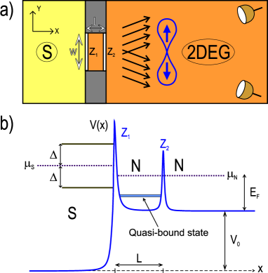
We wish to investigate the role of resonances in the angular distribution of the normal current in suitably designed SSm interfaces. A prototypical structure is shown in Fig. 1a, where the 2DEG forms an angle with the planar boundary of a superconductor, similar to the setup built in Ref. choi05, .
In the present analytical and numerical work we consider a semi-infinite ballistic 2DEG (hereafter also referred to as N) lying in the half-plane . We assume a perfect interface, so that the one-electron potential is independent of . Specifically, is taken of the form
| (1) |
Here, accounts for the large difference between the widths of the S and N conduction bands. If and are N and S Fermi energies, respectively, one typically has , where is the zero-temperature superconducting gap. We assume that the bulk parameters change abruptly at . The structure contains two delta barriers, located at the SN interface and at a distance from it within the N side. Their reflecting power is measured by the dimensionless parameters and , defined as and . The effective mass , the Fermi wavevector , and the Fermi velocity are those of the normal 2DEG, while , , and correspond to a conventional superconductor.
It was shown in Ref. prad04, that the picture of two-electron emission and hole Andreev reflection are equivalent. For computational purposes, we employ here the standard Andreev picture whereby all quasiparticles have positive energy (), with the quasiparticle energy origin given by . However, in our discussion we will occasionally switch between the two images. An important feature is that the absence of a hole at in the Andreev scenario corresponds to the presence of an electron at in the two-electron picture prad04 .
In a transport context, the superconductor and normal metal chemical potentials differ by , where is the applied bias voltage. In the Andreev picture, one artificially takes as the reference chemical potential for labeling quasiparticles and the imbalance is accounted for by introducing an extra population of incoming holes with energies between 0 and blon82 ; lamb91 .
An apparent shortcoming of the Andreev picture is that it does not show explicitly that the emitted electron pairs are internally entangled. In this respect, we may note the following remarks: (i) the two-electron hopping matrix element vanishes when the spin state in the N side is a triplet rech01 ; (ii) an analytical study of transport through a broad SN interface based on a two-electron tunneling picture prad04 (with the final state explicitly entangled) gives results identical to those obtained within an Andreev description kupk97 ; (iii) entanglement in the outgoing electron pairs has been explicitly proven in the general tunneling case samu05 ; and (iv) transport across the SN structure is spin independent and thus must preserve the internal spin correlations of the emitted electron pair oh05 . Moreover, using full counting statistics Samuelsson samu03a has shown that current through an SN double-barrier structure is carried by correlated electron pairs.
To compute the current, we must sum over momenta parallel to the interface, which on the N side take values . For the purposes of solving the one-electron scattering problem, we assume that the superconductor is also two-dimensional. Due to the mismatch in effective masses, the perpendicular energy is not conserved (refraction). The conserved quantum numbers are the parallel momentum () and the total energy (, with ).
For a given , the energy available for perpendicular motion is , where is the electron total energy. As a consequence, for each the picture depicted in Fig. 1b holds provided that the is replaced by an effective value mort99
| (2) |
which is matched to , with generally not equal to .
Beenakker been92 has computed the SN zero bias conductance for an interface with many transverse modes. Mortensen et al. mort99 have adapted the work of Ref. blon82, to account for the full 3D motion through a perfect, 2D SSm interface, where the effective masses and the Fermi wavelengths of N and S may differ widely. Lesovik et al. leso97 have generalized the work of Refs. been92, ; blon82, to the nonlinear case where may be comparable to . They have applied their results to structures displaying quasiparticle resonances. Here we combine the work of these previous three references. Specifically, we investigate the transport properties of an SN interface for arbitrary bias between 0 and . We consider structures displaying resonances due to multiple quasiparticle reflection, and allow for a large disparity between the S and N bulk properties. Most importantly, we calculate the angular distribution of the pair electron current emitted into the semiconductor. Another novel feature is that the semiconductor we consider is a 2DEG whose plane forms an angle with the superconductor planar boundary, so that the SN interface is formed by a straight line.
III Zero bias conductance
The zero bias conductance is defined as
| (3) |
where is the total current at voltage bias . For an SN interface been92 ,
| (4) |
where {} are the eigenvalues of the one-electron transmission matrix through the normal state structure at total energy , and is the number of transverse channels available for propagation in the normal electrode at energy . For a perfect interface, the index runs over the possible values of . Thus, when needed, we make the replacement , where is the interface length. The minimum energy required for propagation in mode , referred to the bottom of the conduction band, is .
In the linear regime, the total energy is restricted to be at . Therefore, the running value of determines the exit angle
| (5) |
since and must satisfy
| (6) |
Therefore, Eq. (4) may be written as
| (7) |
with properly defined as the angular distribution of the zero bias conductance.
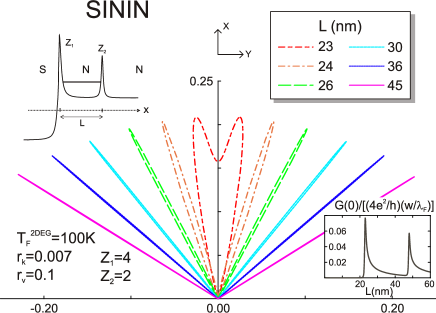
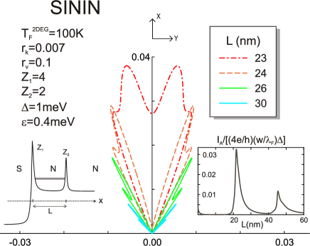
In Fig. 2, we show for several values of the interbarrier distance , on a structure with potential barriers of strength and located at and , respectively. It is divided by ( being the N Fermi wavelength), which is half the maximum possible value of (obtained when for all ).
The semiconductor conduction band width is taken K. The ratios between the Fermi wavevectors and Fermi velocities in N and S are, respectively, and (GaAs values). The presence of quasi-bound states located between the two barriers yields a structure of resonance peaks in the one-electron transmission probability as a function of . We also note that the small value of will cause important internal reflection of the electrons within the superconductor. As a result, only S electrons very close to normal incidence will have a chance to be transmitted into N. Once in N, they may leave with much larger angles. Specifically, if is the angle on the S side, one has (Snell law). For the parameters considered in this article, only electrons arriving from S within degrees of normal incidence are transmitted through the normal-state structure.
As increases, the position of the resonant levels is lowered. In Fig. 2, the values of are chosen such that only the lowest resonant level plays a role. This allows us to investigate the effect of a resonant level at perpendicular energy (on the N side) , which appears as a peak in as a function of . This occurs for satisfying
| (8) |
For the shortest interbarrier distance displayed ( nm), the structure of begins to reveal the presence of a resonance just below . The trend towards a bifurcation of the conductance angular distribution becomes clearer for larger values of . As discussed before, the presence of a sharp resonance only permits the transmission of electrons with perpendicular energy close to . This fixes the value of at and, with it, the magnitude of the exit angle
| (9) |
For a given linewidth of the one-electron resonance, the corresponding spread of the angular distribution is
| (10) |
Thus, the angular width has a minimum at , as in fact revealed by the narrower spikes in Fig. 2.
The lower-right inset of Fig. 2 shows the total conductance [see Eq. (7)] as a function of the interbarrier distance. It is normalized to half its maximum possible value. For small , the lowest resonance lies at , which blocks current flow. As is increased, decreases and the lowest resonance becomes available for transport (). Then shows a rapid increase followed by a decaying tail. The effect is so marked that, if we attempt to plot for e.g. nm (just below the smallest shown value), the resulting curve is invisible on the scale of Fig. 2. As increases further, a second resonance becomes available for transmission and the wide spikes due to the the first resonance coexist with the new, more centered lobes which in turn tend to bifurcate as increases even more (not shown).
The decay of for (where is the interbarrier distance at which ) goes like because it reflects the 1D nature of the transverse density of states. This can be proved by noting that Eq. (4) can be written as
| (11) |
where is the probability for Andreev reflection in mode at total energy , which corresponds to quasiparticle energy . Because of the normal resonance, both and are strongly peaked around the value of satisfying (8). Thus we may approximate , where is an appropriate weight. Then becomes
| (12) |
where is the transverse density of states. On this energy scale, is a smooth function of , so that it can be approximated as , with . Then Eq. (12) yields , as observed in the inset of Fig. 2. Such a manifestation of the transverse density of states in the total transport properties is characteristic of structures which select the energy in the propagation perpendicular to the plane of the heterostructure wagn99 . The foregoing argument allows us to predict that, for a 3D structure, the total conductance will display steps as a function of , since then will be constant (not shown).
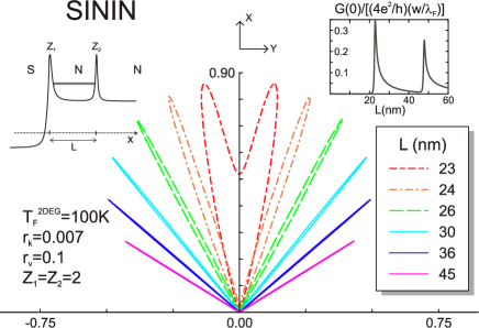
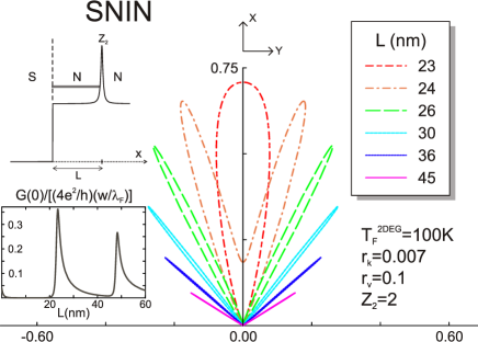
Figs. 3 and 4 show for setups identical to that of Fig. 2, except for taking values 2 and 0, respectively, remaining fixed at 2. The building of SSm interfaces with small seems feasible with the doping techniques implemented in Refs. kast91, ; tabo96, ; giaz03, .
As in Fig. 2, the electron flow is channeled through well-defined resonances in the direction, again giving rise to divergent beams in the N electrode. At first sight it may seem surprising that for one still finds peaks in the angular distribution, since they reveal a structure in the transmission that is not expected from a single barrier of strength . However, when , there is still some normal reflection at due to the large mismatches and . In fact, on quite general grounds, one has as (equivalent to ), even if . This trend is revealed by the decreasing length of the spikes for increasing (decreasing ).
In Fig. 3, stays slightly above for 23 nm. The details of reflection at the interface cause some shift in the detailed position of the resonances. For (Fig. 4), the resonant level at that particular interbarrier distance is exactly at , as revealed by the absence of splitting in . If, by decreasing , were taken considerably above , then the forward lobe of Fig. 4 would be sharply reduced. This general property was already noted in the discussion of Fig. 2 and its inset.
IV Nonlinear transport: spectral conductance
We have seen that, in the zero bias limit, the peaks in the angular distribution directly reflect the structure of (normal) resonances in as a function of , since this determines through Eq. (4). As becomes nonzero and comparable to , new resonances appear which are a direct manifestation of Andreev reflection occurring at nonzero quasiparticle energies. Such Andreev resonances have been discussed, for instance, in Refs. ried93, ; leso97, ; giaz03, . Below we present a brief description that suits our present needs and which complements the discussion given by Lesovik et al. leso97 .
We restrict our study to the case . As in Ref. leso97, , we focus for simplicity on the spectral conductance , i.e. we neglect the contribution to the total differential conductance coming from the derivative with respect to of itself. From Ref. leso97, , we note that, for ,
| (13) | ||||
| (14) |
Here, is the Andreev reflection probability for a quasiparticle of energy incoming in mode , with . It is determined by , which is defined as the transmission probability for an electron incident from the N side on the normal structure (i.e. with ) in transverse mode with total energy , , , and is the phase of the reflection amplitude for an electron impinging from the S side on the normal structure. The latter depends on through the phases acquired upon reflection on each barrier (usually negligible) and, more importantly, through the optical path between the two barriers , where
| (15) |
Here, is the perpendicular velocity for a Fermi electron in mode on the N side (note that is the energy difference between the S chemical potential and the bottom of the N conduction band). We notice the symmetry and the fact that, through (15), the transmission does depend on . In practice, we are only interested in the case . Thus, hereafter we refer to both and as functions of a single argument which is to be identified with in the sense indicated in Eqs. (13) and (14).
The structure of the angular distribution of the conductance reflects that of as a function of , which generally reveals a complex and rich behavior, since it is determined by the combined role of the product and the cosine term in (14). Below we discuss some general trends.
First we note that , with computed for , which is consistent with Eq. (4). If the one-electron (normal) resonance occurs at a perpendicular energy satisfying , for there is always a transverse mode for which
| (16) |
i.e. such that presents a peak at as a function of , with maximum value (normal resonance). In a symmetric structure, .
As a function of , the phases undergo an abrupt change near , so that the cosine term goes quickly through two maxima, in and , none of which necessarily reaches unity. These maxima coincide in general with the peaks of and . From (14), this translates into pairs of close lying peaks in the conductance angular distribution. We have observed that the above tendency is typically present for all intermediate values of (as compared with ) for and . Now we describe another aspect of the peak formation mechanism that is relevant for not much smaller than in the structure . We note that it is compatible with the trend discussed above.
Andreev resonances are characteristically given by the condition leso97
| (17) |
If we recall that is to be identified eventually with , and that through (15) does also depend on , we may state that, for a continuous range of voltages , there is always at least a value of satisfying (17). As defined in (16), is also a function of voltage, since with fixed. Alternatively, one may take as fixed and dependent on voltage; then, is independent of In both scenarios (and, conceivably, in intermediate ones), there is a discrete set of values for which the two transverses modes coincide, i.e. , for which .
We note on the other hand that, for (16) may also be regarded as the maximum condition for viewed as a function of with its maximum lying at (i.e. at total energy ). Thus we can assert that within a range of values, which may include . Noting that the Andreev resonance condition (17) is symmetric in , we conclude from (14) that
| (18) |
even if is not unity. This maximum value of the conductance per mode (which is 2 in units of ; see Ref. sols99, for a discussion) is consistent with the results reported in the single-mode study of Ref. ried93, . Therefore, at voltages the total transmission (summed over ) receives a strong contribution from and its vicinity. This behavior tends to generate peaks in the total spectral conductance at or near the values defined above.
The conclusion is that the sharpest resonances nucleate at angles near normal resonances ( is typically close to , since ). This happens for all energies . However, as explained above, some energies benefit more efficiently from the resonance (in the sense that displays higher maximum values as a function of ) and thus give rise to peaks in when integrated over angles.
Now we may argue like in Section III. Whenever , there is a low-lying transverse mode satisfying (16). Then we expect to have a strong peak in the angular distribution of the spectral conductance, , which is defined to yield
| (19) |
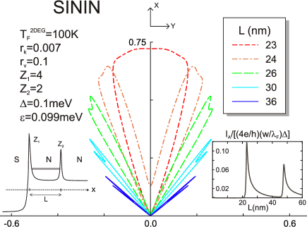
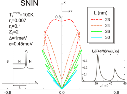
Figs. 5-7 show the normalized value of for structures with and , the former being considered for two different combination of and . As increases, the value of decreases and sinks below . This generates maxima in the angular distribution in the manner discussed above.
At zero temperature, and for , can be understood as the contribution to the total current stemming from electron pairs emitted into the normal metal with total energies . The two electrons leaving the superconductor have identical and slightly different total energy (see below). Thus they do not point exactly in the same direction, i.e. the V which they form upon emission is not exactly centered around the normal axis. By symmetry, for each pair in which e.g. the upper electron is emitted towards the right (and the lower one to the left), there is another pair solution in which the upper electron travels to the left (and the lower one to the right). When plotting the total differential conductance, the two asymmetric Vs appear as a single V whose lobes are double peaked.
We note here that, in the contribution to as defined in Eqs. (13) and (14), is identical to the appearing in the zero voltage limit discussed in the previous section [see Eq. (15)], i.e. as defined in (8), if we identify . This implies that, in the double-peaked lobes, the inner peak points in the same direction as the single-peaked lobe of the linear () limit, a result which is independent of the sign of . The fact that the coincidence occurs at the inner peak can be understood by noting that, since , we have , while . Thus, at a given , peaks in the angular distribution occur at and . Both have the same perpendicular momentum, but the latter has lower parallel kinetic energy.
The fact observed in Figs. 5-7 that the inner peak displays a larger current density is due to the asymmetric character of the peaks in as a function of (or the angle ), which ultimately reflects the greater efficiency with which close-to-normal emission electrons contribute to the electric current.
The insets of Figs. 5-7 show the total current (integrated over and ) as a function of . As for the zero bias conductance, they reveal a succession of maxima followed by an inverse square root decay law that mirrors the transverse density of states (see discussion in the previous section).
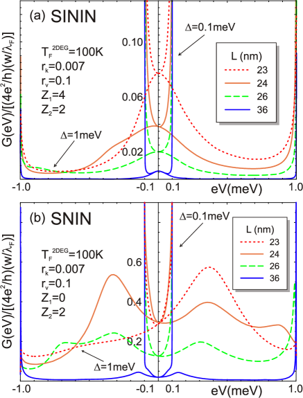
Fig. 8 shows the total spectral conductance for voltages below the gap. This type of curves has been the object of preferential attention in the previous literature on NS transport. By presenting them here, we make connection with that preexisting body of knowledge, in particular with the experimental and theoretical works of Refs. giaz03, and leso97, , respectively. The forthcoming remarks are intended to complement that discussion and to provide a self-contained, unified picture of the work presented here.
The asymmetry in is due to the finite normal bandwidth. For the results plotted in Fig. 8, the voltage varies as varies with fixed. From Fig. 1, it is clear that raising is not equivalent to lowering it. Asymmetric curves are displayed in Ref. choi05, and have been discussed in Ref. leso97, (see also references therein). In what follows, we focus on the behavior for .
Both in Figs. 8a and 8b we present two groups of curves, corresponding to a small and a large gap. The barrier parameters of Fig. 8a are the same as those of Figs. 5 and 6 , namely, . Although Figs. 5 and 6 already exhibit Andreev features such as the double-peaked lobes in , these are washed out when the angular variable is integrated to yield the total spectral conductance , as shown by the single peaked curves obtained for the same value of the gap as in Fig. 5 ( meV), or by the absence of peaks for the parameters of Fig. 6 ( meV. The curves for meV display a clear zero bias conductance peak (ZBCP) whose height is determined by the structure normal properties [see Eq. (4)]. As increases above zero, both electron and holes (or both the upper and lower energy emitted electrons) may benefit from the low-lying normal resonance () as long as , where is the linewidth of the normal resonance. When , it is not possible to channel both electrons through the same resonance and the contribution to the conductances decreases. On closer inspection, one finds that the width of the ZBCP is indeed determined by the normal resonance width, but not by that appearing in the perpendicular transmission (viewed as a function of ). Rather, it essentially mirrors the width of the numerator in Eq. (14). This is the product evaluated at and viewed also as a function of , i.e. for electrons leaving in the direction of maximum current flow (at exit angle ). This is reminiscent of the result stating that, when is replaced by a disordered normal metal, the width of the ZBCP is of the order of the Thouless energy leso97 .
A general property of SN interfaces with a single barrier right at the interface is that Andreev reflection probability tends to unity as blon82 . However, we find that this is generally not the case for a double barrier interface. For , we do notice that sharp peaks in form just below the gap for some values of , so close to it that they can be observed only through a magnification of Fig. 8. Due to this tendency to acquire large values near the gap, goes through a minimum at finite if the width of the ZBCP is smaller than the gap. This is the case shown in Fig. 8a for meV. For a smaller gap ( meV), the value of remains unchanged but there is no room for to display a minimum between 0 and .
Being more transmissive (although not entirely, because of the reflection at the potential step; see Section III), Fig. 8b displays Andreev resonance features that do survive upon integration over angles. For meV and 23 nm, one observes a peak at finite energies that adds to the overall ZBCP. As increases, the inner Andreev peak evolves towards zero energy. At larger distances ( 36 nm), the lowest Andreev resonance can only be hinted at as a shoulder in the plot for meV. We also note that, for 24 and 26 nm, a second Andreev resonance becomes visible close to the gap edge. However, due to the involved interplay between the transmission probabilities and the cosine term appearing in Eq. (14), this second peak does not appear to follow a simple monotonic trend. In fact, for meV, the second resonance is no longer observable because it evolves towards a sharp peak just below the gap.
V Discussion
So far we have assumed that the SN interface is infinitely long (). This has allowed us to treat as a continuous, conserved quantum number, which considerably simplifies the transport calculation. Of course, the idea of an infinite interface is at odds with the primary motivation of our work, which is to propose a method to spatially separate mutually entangled electron beams. Below we argue that, fortunately, only a moderately long interface is needed in practice.
For simplicity, we focus our discussion on the low voltage limit, where the total energy can be assumed to be sharply defined. Then the width of the angular distribution is due only to the uncertainty in the parallel momentum . This in turn is closely connected to through the relation , since total energy uncertainty is zero. There are two contributions to the momentum uncertainty: the nonzero width of the resonance in the perpendicular transmission and the finite length of the SN interface. Thus we may estimate
| (20) |
This translates into an angular width
| (21) |
The actual angular width of is actually a bit smaller, since the present estimate is based on one-electron considerations, while the relevant angular distribution is determined by Eq. (4). We neglect this difference for the present simple estimates.
Eq. (21) contains two contributions. The first term is determined by the normal resonance and is responsible for the width of the angular distributions plotted in Figs. 2-4 (with ). Our main concern here is that the second contribution, that which stems from the finiteness of the aperture, does not contribute significantly.
A strict criterion may be that the interface finite length should not modify the intrinsic angular width (), which everywhere has been assumed to be small enough to allow for narrow divergent beams. A more lenient criterion is that, regardless of the specific value of , the finite aperture should not generate an excessively broad angular distribution. For typical cases this amounts to requiring (for a discussion see Fig. 5 in Ref. prad04, ). For the bandwidth which we have assumed ( K) and an effective mass of , where is the bare electron mass, we have nm. So apertures greater than a few hundred nanometers seem desirable to keep the angular uncertainty within acceptable bounds.
Another source of angular spreading is interface roughness, with a characteristic length scale . However, it should not pose a fundamental problem as long as , so that a structure of intermediate width could be designed satisfying .
For the difference in velocity direction to translate into spatial separation, it is necessary that the spin detectors are placed sufficiently away from the electron-emitting SN interface. Of course, the needed distance depends also on the exit angle . For a convenient value of , simple geometrical considerations suggest that, unsurprisingly, the distance from the detector to the center of the SN interface must be greater than its width . Since elastic mean free paths in a 2DEG can be made as high as 100 m, there seems to be potentially ample room for building structures satisfying . Such devices would display well-defined divergent current lobes which could be detected (and, eventually, manipulated) at separate locations before the directional focusing is significantly reduced by elastic scattering.
VI Conclusions
We have investigated theoretically the possibility of creating hybrid normal-superconductor structures where the two electrons previously forming a Cooper pair in the superconductor are sent into different directions within the normal metal. The central idea relies on the design of a structure that is transparent only to electrons with perpendicular energy within a narrow range of a resonant level. Since the total energy lies close to the Fermi level, such a filtering of the electron perpendicular energy translates into exit angle selection.
Electrons from a conventional superconductor are known to be correlated in such a way that electrons moving at similar speeds in opposite directions tend to have opposite spin. At low temperatures and voltages, electron flow from the superconductor to the normal metal is entirely due the transmission of correlated electron pairs. These have both opposite spin and opposite parallel (to the interface) momentum, while possessing the same total energy. If the exit angle is selected by filtering the perpendicular momentum, the current in the normal metal is formed by two narrow, mutually singlet entangled electron beams which point in different directions and which spatially separate from each other at distances from the source much greater than the width of the source.
The trick of exit angle selection is intended to facilitate a neat observation of nonlocal entanglement between electron beams, and this article has been devoted to proposing a specific implementation of that idea. One cannot help noting, however, that such a selection of the outgoing direction might not be totally essential. If we content ourselves with measuring anticorrelated low-energy spin fluctuations over mesoscopic length scales, it may just be sufficient to place the two spin detectors symmetrically around the interface at a sufficient distance and angle, very much like in the setup of Fig. 1a but with a conventional, non angle-selecting SN tunnel interface. If their motion between the emitter and the detector is ballistic, electrons arriving at each detector have, on average, opposite parallel momentum and opposite spin (angular anticorrelation has been explicitly shown in Ref. prad04, for a broad perfect interface). The boundaries of the 2DEG might conceivably be designed to optimize such correlations. The outcome is that electrons arriving at each detector will exhibit a degree of nonlocal spin-singlet correlations that could be measured.
Altogether, we conclude that a ballistic two-dimensional electron gas provides an ideal scenario to probe nonlocal entanglement between electrons emitted from a distant, finite-size interface with a superconductor. If that interface is formed by a hybrid structure that selects the perpendicular energy and thus the magnitude of the electron exit angle, nonlocal spin correlations will be clearly observed if the outgoing beams are directed towards suitably placed detectors.
Acknowledgments
This research has been supported by MEC (Spain) under Grants No. BFM2001-0172 and FIS2004-05120, the FPI Program of the Comunidad de Madrid, the EU Marie Curie RTN Programme under Contract No. MRTN-CT-2003-504574, and the Ramón Areces Foundation.
References
- (1) P. Recher, E.V. Sukhorukov, and D. Loss, Phys. Rev. B 63, 165314 (2001).
- (2) G.B. Lesovik, T. Martin, and G. Blatter, Eur. Phys. J. B 24, 287 (2001).
- (3) P. Recher and D. Loss, Phys. Rev. B 65, 165327 (2002).
- (4) N.M. Chtchelkatchev, G. Blatter, G.B. Lesovik, and T. Martin, Phys. Rev. B 66, R161320 (2002).
- (5) D. Feinberg, Eur. Phys. J. B 36, 419 (2003).
- (6) P. Recher and D. Loss, Phys. Rev. Lett. 91, 267003 (2003).
- (7) P. Samuelsson, E. V. Sukhorukov, and M. Büttiker, Phys. Rev. Lett. 91, 157002 (2003).
- (8) E. Prada and F. Sols, Eur. Phys. J. B 40, 379 (2004).
- (9) P. Samuelsson, E.V. Sukhorukov, and M. Büttiker, Phys. Rev. B 70, 115330 (2004).
- (10) R. Mélin and D. Feinberg, Phys. Rev. B 70, 174509 (2004).
- (11) O. Sauret, D. Feinberg, and T. Martin, Phys. Rev. B 70, 245313 (2004).
- (12) A. F. Andreev, Zh. Eksp. Teor. Fiz. 46, 1823 (1964).
- (13) P. Samuelsson, E.V. Sukhorukov, and M. Büttiker, New J. Phys. 7, 176 (2005).
- (14) F. W. J. Hekking and Y. Nazarov, Phys. Rev. Lett. 71, 1625 (1993); Phys. Rev. B 49, 6847 (1994).
- (15) D. Beckmann and H.B. Weber, Phys. Rev. Lett. 93, 197003 (2004).
- (16) S. Russo, M. Kroug, T. M. Klapwijk, and A. F. Morpurgo, Phys. Rev. Lett. 95, 027002 (2005).
- (17) P. Aronov and G. Koren, cond-mat/0508753.
- (18) M. Houzet, D. A. Pesin, A. V. Andreev, and L. I. Glazman, Phys. Rev. B 72, 104507 (2005).
- (19) V. Bouchiat et al., Nanotechnology 14, 77 (2003).
- (20) G. Bignon, M. Houzet, F. Pistolesi and F. W. J. Hekking, Europhys. Lett. 67, 110 (2004).
- (21) L. L. Chang, L. Esaki, and R. Tsu, Appl. Phys. Lett. 24, 593 (1974); F. Capasso and S. Datta, Phys. Today 43, 74 (1990).
- (22) P. G. de Gennes and D. Saint-James, Phys. Lett. 4, 151 (1963).
- (23) R. A. Riedel and P. F. Bagwell, Phys. Rev. B 48, 15198 (1993).
- (24) F. Giazotto et al., Phys. Rev. Lett. 87, 216808 (2001).
- (25) F. Giazotto, P. Pingue, and F. Beltram, Mod. Phys. Lett. B 17, 955 (2003).
- (26) T. Akazaki, J. Nitta, and H. Takayanagi, Appl. Phys. Lett. 59, 2037 (1991).
- (27) A. Kastalsky et al., Phys. Rev. Lett. 67, 3026 (1991).
- (28) J. R. Gao et al., Appl. Phys. Lett. 63, 334 (1993).
- (29) C. Nguyen, H. Kroemer, and E. L. Hu, Appl. Phys. Lett. 65, 103 (1994).
- (30) R. Taboryski et al., Appl. Phys. Lett. 69, 656 (1996).
- (31) S. De Franceschi et al., Appl. Phys. Lett. 73, 3890 (1998).
- (32) E. Toyoda, H. Takayanagi, and H. Nakano, Phys. Rev. B 59, R11653 (1999).
- (33) I. E. Batov, Th. Schäpers, A. A. Golubov, and A. V. Ustinov, J. Appl. Phys. 96, 3366 (2004).
- (34) B. R. Choi et. al., Phys. Rev. B 72, 024501 (2005).
- (35) H. van Houten et al., Europhys. Lett. 5, 721 (1988).
- (36) E. I. Rashba, Fiz. Tverd. Tela (Leningrad) 2, 1224 (1960) [Sov. Phys. Solid State 2, 1109 (1960)].
- (37) S. Datta and B. Das, Appl. Phys. Lett. 56, 665 (1990).
- (38) J. Schliemann, J. C. Egues, and D. Loss, Phys. Rev. Lett. 90, 146801 (2003).
- (39) C.W.J. Beenakker, C. Emary, M.Kindermann, and J.L. van Velsen, Phys. Rev. Lett. 91, 147901 (2003).
- (40) L. Faoro, F. Taddei and R. Fazio, Phys. Rev. B 69, 125326 (2004).
- (41) O. Sauret, T. Martin, and D. Feinberg, Phys. Rev. B 72, 024544 (2005).
- (42) E. Prada, F. Taddei and R. Fazio, Phys. Rev. B 72, 125333 (2005).
- (43) F. Taddei, L. Faoro, E. Prada and R. Fazio, New J. Phys 7, 183 (2005).
- (44) J. Torrès and T. Martin, Eur. Phys. J. B 12, 319 (1999).
- (45) G. Burkard, D. Loss, and E. V. Sukhorukov, Phys. Rev. B 61, R16303 (2000).
- (46) P. Samuelsson and M. Büttiker, Phys. Rev. Lett. 89, 046601 (2002).
- (47) N. A. Mortensen, K. Flensberg, and A. P. Jauho, Phys. Rev. B 59, 10176 (1999).
- (48) C. W. J. Beenakker, Phys. Rev. B 46, 12841 (1992).
- (49) G. B. Lesovik, A. L. Fauchere, and G. Blatter, Phys. Rev. B 55, 3146 (1997).
- (50) J. A. Melsen and C. W. J. Beenakker, Physica B 203, 219 (1994).
- (51) G. E. Blonder, M. Tinkham, and T. M. Klapwijk, Phys. Rev. B 25, 4515 (1982).
- (52) C. J. Lambert, J. Phys. Condens. Matter 3, 6579 (1991).
- (53) M. Kupka, Phys. C 281, 91 (1997).
- (54) S. Oh and J. Kim, Phys. Rev. B 71, 144523 (2005).
- (55) P. Samuelsson, Phys. Rev. B 67, 054508 (2003).
- (56) M. Wagner and F. Sols, Phys. Rev. Lett. 83, 4377 (1999).
- (57) F. Sols and J. Sánchez-Cañizares, Superlatt. and Microstruct. 25, 627 (1999).