Current-Voltage Characteristics in Donor-Acceptor Systems : Implications of a Spatially varying Electric Field
Abstract
We have studied the transport properties of a molecular device composed of donor and acceptor moieties between two electrodes on either side. The device is considered to be one-dimensional with different on-site energies and the non-equilibrium properties are calculated using Landauer’s formalism. The current-voltage characteristics is found to be asymmetric with a sharp Negative Differential Resistance at a critical bias on one side and very small current on the other side. The NDR arises primarily due to the bias driven electronic structure change from one kind of insulating phase to another through a highly delocalized conducting phase. Our model can be considered to be the simplest to explain the experimental current-voltage characteristics observed in many molecular devices.
The study of electron transport through single molecules is gaining tremendous attention in recent years owing to the wide variety of applications that they can be used inrev . Recent advances in experimental techniques have allowed fabrication and measurement of current through such nanoscale systems. Various molecular systems have already been demonstrated to behave as wires, switches, diodes and RAMsreed ; Cui ; Kushmerick . The ability of a molecule to switch between off and on states is one of its most important applications. Experimentally, this has been observed in several organic molecules with various donor and acceptor substituents Tour ; Donhauser ; exptNDR ; Xiao . Considerable amount of theoretical work based on semi-empirical to ab-initio methods have also been performed to model molecular transport characteristicsrev . Many explanations for this switching phenomenon, based on chargingSeminario ; 2site , reduction of the acceptor moiety Xiao , twisting of the ring structure leading to conformational changesTaylor ; Bredas ; Ranjit ; lakshmi , bias driven changes in molecule-electrode couplingXshi , have been proposed. Most of these require to impose some external factor like the rotation of the middle ring etc in order for the external bias to cause NDR at some bias. And most often they do not make a relation between structural preference and bias polarity and hence do not explain the asymmetry that has been observed in the experiments. Also a comprehensive understanding of the switching phenomena in general cases is still elusive.
In this letter, we try to understand the reasons for the observed Negative Differential Resistance (NDR) in molecular wires based on a very simple donor-acceptor model. In fact, the asymmetry as well as NDR in forward bias that has been observed in the Tour moleculesreed ; Tour comes out naturally out of this dimer model without having to invoke any external factors. And the simplicity of this parametrized model makes it very tractable and lends physical insight into the factors causing the NDR. We find that a spatially varying external forward bias switches the electronic phases resulting in a sharp rise and fall in transmission through the device. Various extensions of the dimer model together with different spatial variations of the electrostatic potentials have also been considered.
A closer look at the structure of the Tour molecules (see inset of Fig.1) suggests that one part of the molecule with the donor group (NH2) has a positive on-site energy and the other with acceptor group (NO2) has a negative on-site energy (Although this has been assumed here, we have later extended it to describe systems with many localized segments in it, as is shown by quantum chemical calculations on the Tour molecules). For such a two-level model involving a donor and an acceptor, the Hamiltonian is given as: , where is the on-site energy of site and is the hopping integral. This dimer is attached to two metallic electrodes on either side, which are assumed to be non-interacting semi-infinite one dimensional systems described by a tight-binding Hamiltonian with an energy bandwidth of where eVmujica2 . The Fermi energy of the electrodes is generally assumed to be a fitting parameter. We assume that the Fermi energy lies halfway between these equilibrium (zero bias) energies, though its location does not influence our main results.
Spatial variation of bias on the structure is quite a central issue in this fieldSdatta . Except for a few cases (given later), we consider that it drops on the device as a ramp function, varying linearly from one electrode to the other as: , where n is the site-index and N, the total number of sites. With the potential, the energies for the dimer can be written as:
| (1) | |||||

The coupling to the electrodes modifies the bare Greens function of the molecule, which across the molecule can be written as
| (2) | |||||
where and are the self-energies corresponding to the two electrodes, calculated within the Newns-Anderson modelNewns . Using the Greens function, the current through the system can be obtained from the Landauer’s formula datta_book :
| (3) |
where are the anti-hermitian parts of the self-energy matrices, which describe the broadening of the energy levels due to the coupling to the electrodes.
In zero bias condition, as can be seen from Eq.1 (with ), presence of different on-site energies opens up a gap larger than that for a purely hopping model () near the zero of energy indicating the preference of the electrons to stay at the atomic site with negative on-site energy. The equilibrium transmission is found to be large for purely hopping model since it corresponds to equal distribution of charges. With the inclusion of different on-site energies, the systems becomes insulating due to charge transfer and the zero-bias transmission reduces due to this preferential charge localization.

Fig 1 shows the nature of the current-voltage characteristics with external bias. As can be seen, the current is negligible around the zero of energy and around a bias of , there is a small jump in the current. This is the bias at which the device energy level comes into resonance with the Fermi energy of the electrodesmujica2 . With increase in the forward bias, around a bias of , the current shows a sharp rise and fall, indicating strong Negative Differential Resistance (NDR). On the other hand, with increase in the reverse bias, the system continues to remain insulating with negligible current.
To understand the reasons for the NDR, we look at the variation of the energy levels () of the bare molecular dimer with bias (Fig 2a) and the numerator of the Greens function, (see Fig 2b, are the eigenstates). With increase in the forward bias, the energy levels come close to one another up to the critical bias at which the NDR is seen, above which, they move farther away. In Fig. 2b, exactly around this , the contribution to the eigenstate (MO) coefficients from the sites increases quite sharply. To quantify this critical bias , we minimize the gap between the energies with respect to the applied bias and obtain, , which is in accordance with our numerical data (for and , we find ) Pearson . At this critical bias, the energies take the values , precisely the energies of the non-interacting system. However, with increase in the reverse bias, the energy levels start diverging away from their zero bias gap making the system more and more insulating, explaining the small current that is observed in Fig.1 for negative bias.
To quantify the effect at , we calculate the Average Inverse Participation Ratio () which defines the extent of localization for a given eigenstate, with :
| (4) |
where is the IPR, defined as where the is the atomic site index and is the density of states. Fig. 2c shows a strong dip in the values of around the critical bias indicating complete delocalization in the system, while at other values of the bias, is much larger due to the localized nature of the eigenstates.
Initially for small bias, as noted before, the system tends to accumulate its charge density at the site with lower on-site energy. Such a localization causes the system to be insulating. If this site is closer to the electrode with higher chemical potential, charges tend to move towards the other site. At , where the NDR is seen, the charge densities are equally distributed at both sites with no preference of one site over another indicating a situation where both the on-site energies are equal. Further increase of bias would localize the charges on the other site resembling an insulating dimer with its on-site energies interchanged, precisely the case as with reverse bias.
To extend these dimer results further, we look at a chain of atoms with alternating on-site energies, and . The energies in the absence of external bias have the form:
| (5) |
where N is the number of sites and the ’’ signs hold for j=1,2…., (j=+1,…..N). It is quite well-known that different diagonal terms (either random or alternating) localizes the eigenstates of a one-dimensional system. From a perturbative treatment, this localization can be made quantitative as mujica2 , where the localization length depends on the width of the diagonal term and the hopping . Since the system becomes highly delocalized at , we can naively expect the width to tend to zero at this bias, giving , for a sites chain.
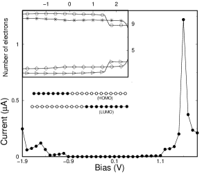
For a 20 sites half-filled system, we obtain a of for values of and and , which is close to the value calculated from the above expression (), with second-order corrections due to the hopping term Pearson . Fig 3 shows the I-V characteristics for this system which is asymmetric and shows clear eigenvalue jumps for reverse biasndr_reverse and a sharp NDR peak at a critical forward bias.
To quantify the effect of bias in the system, we calculate the total charge densities in each of the two sub-lattices for two cases: (i) charges are filled up to the highest-occupied level (HOMO) and (ii) with one of the highest occupied level electron promoted to the lowest unoccupied level(LUMO). Both of these, for each sub-lattice are plotted in the inset of Fig.3, as a function of external bias. As can be seen, there is a jump in the charge density in the sub-lattice due to the initiation of charge transfer from sub-lattice to the sub-lattice with , exactly at the critical bias. Since the HOMO and LUMO levels are very close in energy at the critical bias (as shown for the 2-level system in Fig.2), the charge densities corresponding to both cases become equal for each sub-lattices, giving rise to the crossing of the respective curves. We have also shown in the figure, a pictorial representation of the HOMO and LUMO eigenstates close to . As can be seen, the contribution to HOMO primarily comes from one end of the chain and to LUMO from the other end. However, since at these two states are quasi-degenerate, a linear combination of the two correspond to a system with large transmission amplitude between two ends.

As is well-known, due to screening effects, the potential gradient is expected to be larger near the electrodes than at the center of the chain where it may be zero or very smallSdatta . We have considered the spatial variation of the potential over sites close to the interface with variation in , and the potential is a ramp function when . Three different potential drops have been considered: (a) ramp (b) (2 sites drop) and (c) ( 8 sites drop) close to the interface. In Fig 4., we have plotted the I-V characteristics for the system with and for all the three cases. For the one with , the I-V curves shows clear eigenvalue jumps. With the increase in , the NDR begins to appear at smaller voltages, and a very sharp NDR peak is seen for the ramp potential. The inset shows the variation of the HOMO-LUMO gap with bias for the three cases. There is no significant closing in of the levels when . But with increasing , this becomes more and more pronounced and the NDR appears earlier and is sharper. This study indicates the importance of the spatial variation of the applied electric field in order to see an NDR response.
In the long-chain limit, there is an implicit relation between variation in on-site energies and the bond-length alternation (BLA). Almost all the Tour molecules have BLA together with donor and acceptor groups. In fact, the BLA which dimerizes the system have been shown to give rise to NDRlakshmi . Interestingly, we find that donor () and acceptor () at some positions together with explicit dimerization also causes NDR and asymmetric I-V, very similar to the I-V shown in Fig.3. The main point is that whether it is the explicit dimerization or two-sublattice structure, coupled with the voltage drop, it induces interchange of symmetry together with Landau quasi-degeneracy of the low-lying levels.
To summarize, we find that the ratio is very crucial in determining the nature of the I-V characteristics. Three features, namely, the critical bias, the sharpness of the NDR peak and the extent of asymmetry in the I-V curves are sensitive to this ratio. We believe this to be the reason for experimentally observed NDR and asymmetry in Tour molecules containing NH2 and NO2 groups or NO2 group only, and its absence when there is only NH2 group or no substituents. Nitro group, having a very strong acceptor character tilts this ratio in favor of a sharp NDR peak and asymmetry, within the bias range considered.
Although our model neglects some of the important issues in this field like electron-electron interactions, Coulomb blockade, and other many-body effects, it is nevertheless interesting to see how some experimentally observed features can be captured even by such simple models. And a two-level model, although not well-supported by quantum chemical calculations, is not too far-fetched a description of the Tour molecules, in which the strength of the localized donor/acceptor reduces progressively towards the chain ends.
Our explanation for NDR encompasses the bias driven conformational change occurring in the system and the reduction of the acceptor to donor, where the roles of the donor and acceptor groups have been interchanged, as well as the bias driven changes in electrode-molecule coupling which would result in a change in the on-site energies of the components of the molecule. However, the common thread among all the known factors governing NDR requires further attention.
SKP acknowledges the DST, Govt. of India for financial support.
References
- (1) A. P. Alivisatos et al, Adv. Mater. 10, 1297 (1998); F. Zahid, M. Paulsson and S. Datta, in Advanced Semiconductors and Organic Nano-Techniques, ed. by H. Morkoc, Academic Press, 2003.
- (2) M. A. Reed et al, Science 278, 252 (1997); Appl. Phys. Lett. 78, 3735 (2001).
- (3) X. D. Cui et al, Science 294, 571 (2001).
- (4) J. G. Kushmerick et al, Phys. Rev. Lett. 89, 086802 (2002).
- (5) J. Chen et al, Science, 286, 1550 (2001); Appl. Phys. Lett. 77, 1224 (2000).
- (6) Z. J. Donhauser et al, Science, 292, 2303 (2001).
- (7) I. Kratochvilova et al, J. Mater. Chem. 12, 2927 (2002); N. P. Guisinger et al, Nano Lett. 4, 55 (2004).
- (8) X. Xiao et al, J. Am. Chem. Soc. 127, 9235 (2005).
- (9) J. M. Seminario, A. G. Zacarias and J. M. Tour, J. Am. Chem. Soc. 122, 3015 (2000); J. M. Seminario, A. G. Zacarias and P. A. Derosa, J. Chem. Phys. 116, 1671 (2002).
- (10) J. E. Han and V. H. Crespi, Appl. Phys. Lett. 79, 2829 (2001).
- (11) J. Taylor, M. Brandbyge and K. Strokbro, Phys. Rev. B. 68, 121101 (2003).
- (12) Y. Karzazi, J. Cornil and J. L. Bredas, J. Am. Chem. Soc. 123, 10076 (2001).
- (13) R. Pati and S. P. Karna, Phys. Rev. B. 69 155419 (2004).
- (14) S. Lakshmi and Swapan K. Pati, J. Chem. Phys. 121, 11998 (2004).
- (15) X. Shi, X. Zheng, Z. Dai, Y. Wang and Z. Zeng, J. Phys. Chem. B. 109, 3334 (2005)
- (16) Y. Karzazi, J. Cornil and J. L. Bredas, Nanotechnology 14, 165 (2003); S. Lakshmi, A. Datta and S. Pati, Phys. Rev. B72, 045131 (2005).
- (17) V. Mujica, M. Kemp, A. E. Roitberg and M. A. Ratner, J. Chem. Phys. 104, 7296 (1996).
- (18) P. W. Anderson, Phys. Rev., 124, 41 (1961); D. M. Newns, Phys. Rev., 178, 1123 (1969).
- (19) S. Datta et al, Phys. Rev. Lett. 79, 2530 (1997); V. Mujica, A. E. Roitberg and M. A. Ratner, J. Chem. Phys. 112, 6834 (2000); S. Pleutin, H. Grabert, G-L Ingold and A. Nitzan, J. Chem. Phys. 118, 3756 (2003).
- (20) S. Datta, Electronic Transport in Mesoscopic Systems (Cambridge Univ. Press, New York, 1996).
- (21) R. G. Pearson, Inorg. Chem. 27, 734 (1988); Using the values of the absolute electronegativities and hardness, the ionization potential difference between amino and nitro group is calculated to be of the order of 1.0eV. Critical bias calculated from this, gives a resonable comparison with experiments.
- (22) We also see an NDR peak at reverse bias region (at compared to in forward bias). This is because in the reverse bias, the charge movement is opposed by the extra hopping term which arises due to the even number of sites in the chain. The difference between the critical bias in the positive and negative direction is governed dominantly by and to a second order by the difference in the . Note that, NDR on both sides of bias has been observed in an experiment with Tour molecule recentlyXiao .