PHYSICAL REVIEW B 71, 195301 (2005) also appears in VIRTUAL JOURNAL OF ULTRAFAST SCIENCES (JUNE 2005)
Three-dimensional carrier-dynamics simulation of terahertz emission from photoconductive switches
Abstract
A semi-classical Monte Carlo model for studying three-dimensional carrier dynamics in photoconductive switches is presented. The model was used to simulate the process of photo-excitation in GaAs-based photoconductive antennas illuminated with pulses typical of mode-locked Ti:Sapphire lasers. We analysed the power and frequency bandwidth of THz radiation emitted from these devices as a function of bias voltage, pump pulse duration and pump pulse location. We show that the mechanisms limiting the THz power emitted from photoconductive switches fall into two regimes: when illuminated with short duration () laser pulses the energy distribution of the Gaussian pulses constrains the emitted power, while for long () pulses, screening is the primary power-limiting mechanism. A discussion of the dynamics of bias field screening in the gap region is presented. The emitted terahertz power was found to be enhanced when the exciting laser pulse was in close proximity to the anode of the photoconductive emitter, in agreement with experimental results. We show that this enhancement arises from the electric field distribution within the emitter combined with a difference in the mobilities of electrons and holes.
pacs:
42.72.Ai, 73.20.Mf, 78.20.Bh, 78.47.+pI Introduction
Over the last few years interest in using far-infrared radiation as a non-contact probe of the properties of various materials such as semiconductors Huber et al. (2001); Leitenstorfer et al. (2002); Kaindl et al. (2003), superconductors Nuss et al. (1991); Gao et al. (1995); Federici et al. (1992) and biological tissue Han et al. (2000); Pickwell et al. (2004) has grown considerably. This has been as a result of improvements in sources Shen et al. (2003); Johnston et al. (2002) and detectors Shen et al. (2004) of terahertz (THz) frequency radiation, and the development of novel spectroscopic methods such as time domain spectroscopy Ferguson and Zhang (2002); Shan et al. (2002). By recording the electric field of a single cycle of terahertz radiation as function of time, the technique of time domain spectroscopy is capable of extremely sensitive measurements, especially in the far-infrared band. This technique represents a particularly powerful tool for studying the dynamics of weakly correlated systems in condensed matter physics, including excitons and Cooper pairs, which have binding energies observable in the THz region of the electromagnetic spectrum Kaindl et al. (2003); Federici et al. (1992).
Terahertz time domain spectroscopy relies on the ability to produce pulses of THz radiation so short that they contain only one or even half a cycle. Single-cycle THz pulses can be generated by shining ultrashort laser pulses on bulk semiconductors such as InAs, GaAs and GaP Held et al. (1991); Johnston et al. (2002). These pulses contain a continuous and broad distribution of frequencies, which can be exploited to perform spectroscopic studies over a large portion of the spectrum.
In bulk semiconductors single-cycle radiation can be emitted via three mechanisms: the formation of an electrical dipole due to the difference of mobilities between electrons and holes (the photo-Dember effect) Johnston et al. (2002), optical rectification Auston and Cheung (1985), and the acceleration of charges under the surface depletion field of a semiconductor Johnston et al. (2002). Photoconductive switches (PCSs) are an attractive alternative to surface field semiconductors emitters for the production of single-cycle THz radiation Smith et al. (1988). These devices have been shown to produce broad bandwidth THz signals with high electric field intensities Shen et al. (2003). In a PCS two parallel metallic contacts are deposited on the surface of a semiconductor, an external biasing voltage is applied between these contacts and an ultra-short laser pulse is used to generate photo-carriers in the gap between the contacts. The acceleration of these carriers by the external electric field gives rise to an electromagnetic emission according to Maxwell’s equations.
An understanding of the carrier dynamics in photo-conductive switches is of major importance in order to improve the bandwidth and power of these devices. Several theoretical and experimental studies have been performed to understand different aspects of the process of THz emission by PCS. These works include the analysis of charge transport by the use of rate equations Rodriguez et al. (1994); Dekorsy et al. (1993) and Drude-Lorentz models Piao et al. (2000); Jepsen et al. (1996). In addition, the effect of dislocations on the emitted signal has been studied by the inclusion of reduced mobilities in rate equations Liu and Qin (2003a) as well as experimentally measuring time domain THz traces and fitting them to simple charge transport models Nemec et al. (2001). Also, TDS experiments using double pulses to excite the PCS Siebert et al. (2004) have been performed to obtain information about the photo-generated carrier screening of the bias voltage.
These models correctly predict most of the characteristics of the observed THz signals, but have the disadvantage that parameters such as mobility and carrier trapping time have to be adjusted phenomenologically to reproduce the details of the experimental measurements. While such models have the advantage that under certain circumstances they can be analytically solved, this possibility is limited by factors such as the geometry of the domain in which the equations can be solved, and in some cases the analysis has to be restricted to one or two dimensions Dekorsy et al. (1993); Nemec et al. (2001); Rodriguez and Taylor (1996). A Monte Carlo simulation for PCSs was recently published Liu and Qin (2003b) that models the dynamics of a low density of electrons generated by small photon fluences. However, it neglects the contribution of holes to the current density (see Section II) as well as the carrier-carrier scattering mechanism which has been found to dominate the total carrier scattering rate Lloyd-Hughes et al. .
In this work a three-dimensional Monte Carlo model is presented (Section II) that provides a powerful tool for the analysis of the influence of parameters on carrier dynamics and the evolution of variables in time. The effect of the applied bias voltage (Section III) and pump pulse width (Section IV) on the emitted signal is analyzed. A discussion of electric field screening is also presented (Section V).
II Monte Carlo Model
In this paper we extend the Monte Carlo model of Ref. Johnston et al. (2002) to simulate emission from PCSs. The model uses the current density vector as source term of Maxwell’s equations. The electric field is calculated by the use of the far-field approximation
| (1) |
In order to obtain the current density vector, the simulation volume is divided into a three-dimensional rectangular grid, and the displacement of each carrier (electron or hole) is calculated over small time intervals, which are shorter than the scattering times. In each time interval and spatial box, the electric field is assumed to be constant and uniform and then the displacement of each carrier is calculated by assuming it follows the solution of
| (2) |
with initial conditions given by its previous position and velocity, where is the acceleration of the carrier with charge and effective mass in an electric field .
Although the simulation assumes parabolic band dispersion, inclusion of both and L valleys creates a more realistic carrier ensemble. A set of quantum mechanical scattering rates are calculated. Random numbers are used to determine if each particle is scattered in each time step, the scattering angle and the energy loss. The scattering mechanisms included are: LO phonon absorption and emission within both and L valleys, TO phonon emission and absorption between and L valleys, acoustic phonon, impurity and carrier-carrier scattering. Details of the implementation of these scattering mechanisms are described in Ref.Johnston et al. (2002).
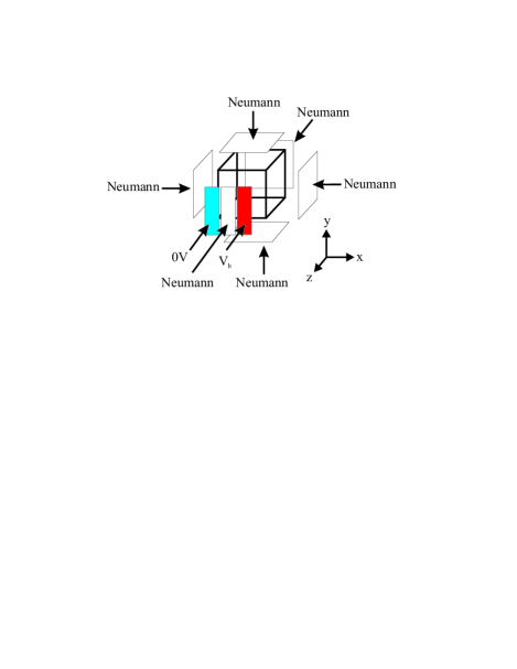
In each time interval the charge density is calculated for each of the boxes in the spatial grid. This is then used to find the electric potential by numerically solving Poisson’s equation in three dimensions using a relaxation method with Chebyshev acceleration. The boundary conditions for solving Poisson’s equation are set as follows (Fig. 1): the potential is fixed to zero on one third of the top surface (), corresponding to one of the contacts, on the second third of the surface Neumann boundary conditions are assumed, and the potential is fixed to (the bias voltage) in the final third. Neumann boundary conditions are also assumed on the other boundaries. The electric-field vector , is determined using the central difference method. Initially the spatial distribution of extrinsic carriers is calculated, and the temperature distribution of these cold carriers is set according to Maxwell-Boltzman statistics. The simulation is run until charge distribution equilibrium is reached, prior to the photo-excitation process.
Photo-excited carriers are assumed to be generated according to the spatial and temporal intensity of a Gaussian laser pulse absorbed in the sample. Random numbers are used to calculate the initial positions of each photo-generated electron-hole pair. The distribution in the -direction is weighted exponentially as defined by the absorption coefficient of the light in the semiconductor. The initial energy of the electron-hole pairs is the difference between the semiconductor band gap and the photon energy, this energy is partitioned between electrons and holes based on momentum conservation. Photons are assumed to have the energy distribution of a Gaussian pulse (thus spectral width in the simulation is calculated from the laser pulse duration parameter). The directions of the pairs of momentum vectors are initially randomized with equal probability across steradians.
The net current density vector is then calculated as
| (3) |
its derivative is calculated and with it the radiated electric field using the far field approximation (Equation 1).
The parameters used in the simulation are taken from Ref. Johnston et al. (2002). These parameters are typical of insulating GaAs (an n-type sample with very low donor density of was chosen). A 4 pJ laser pulse with standard deviation beam-waist was simulated, where the centre wavelength of the laser pulse was chosen to be 800nm (1.55 eV). The domain of the simulation was , divided in to a space-grid of and time intervals of . The distance between the contacts of the simulated photoconductive switch was . One million pairs of pseudo-particles were used to represent extrinsic and intrinsic electrons and holes.
III Bias voltage effects
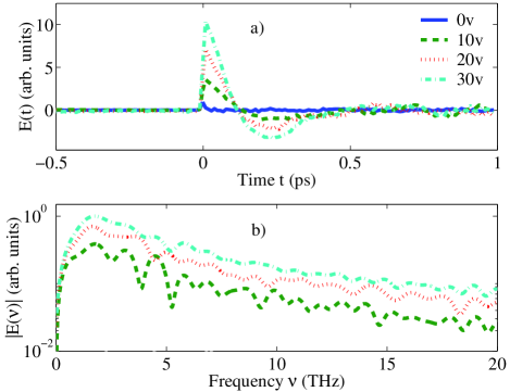
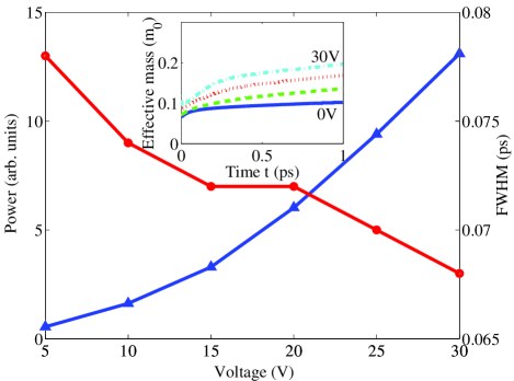
Using the model described in the previous section we performed a study of the effect of applied bias voltage on emitted THz power from GaAs PCSs. Since mode-locked Ti:Sapphire lasers are most commonly used in experiments we chose pulse parameters typical of this type of laser. The simulation results presented in Fig. 2a show the effect of altering the bias across a PCS. In this set of simulations the laser pulse duration was set to 10 fs, which is a pulse duration easily achieved using chirped mirror Ti:Sapphire oscillators. The THz pulse shortens at higher bias voltages as seen in Fig. 3, in which the FWHM of the pulses at different voltages are plotted. This is because at higher applied voltages a greater number of electrons are transferred into the L-valley, resulting in a higher TO-phonon emission and absorption rate. As a consequence the average effective mass of the electron population increases (see inset in Fig. 3), reducing the net electron mobility, thereby shortening the pulse. This effect has been observed in the experiments of Liu et al. Liu et al. (2003). In Fig. 2b the Fourier transforms of Fig. 2a are shown. These spectra broaden as the voltage increases, produced by the shortening of the THz transient.
The power emitted increases with the bias voltage, as seen in Fig. 3, and in agreement with the experimental measurements of Liu et al. (2003). This power enhancement is expected in a simple macroscopic picture. Taking the current vector , with being the switch’s conductivity and the external bias field, assuming that remain constant we get . If the power is given by
| (4) |
and since we end up with , which is consistent with the quadratic-like behaviour of power in Fig. 3. Note that the assumption of being constant, while a good first approximation, it is not strictly true as shown by the further analysis of the full microscopic simulation (Section V).
IV Pulse width effects
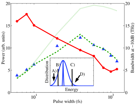
The excitation pulse duration is one of the main variables affecting the temporal width (and hence the frequency bandwidth) of an emitted THz transient from a photoconductive switch. This is primarily because the pulse duration determines the time interval over which photo-carriers are generated, and therefore the current rise time in a PCS. Here we present a set of simulations where the excitation pulse duration is varied over a range achievable using Ti:Sapphire lasers (6 to 120 fs).
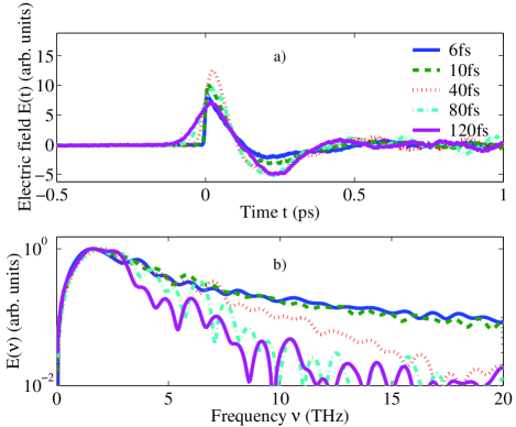
In Fig. 4 the electric fields for various laser pulse durations are shown for a bias voltage of . It can be seen that the THz transient becomes narrower as the pump pulse gets shorter (Fig. 4a). In Fig. 4b the spectra of the time-domain pulses are shown. While the distributions for long pump pulses () show a sudden drop in spectral components over , distributions for short pulses () contain components over . The distribution width at -10dB of the spectra is used as a measure of the bandwidth of signal generated in the PCS in Fig. 5. This plot shows how the bandwidth of the signal increases as the pump pulse shortens.
A priori the power is not expected to depend significantly on the exciting pulse width, as the number of photons per pulse and the applied bias voltage are identical in the simulation. In Fig. 5 the power is plotted (triangles) as function of the pump pulse width. Surprisingly a strong dependence can be seen, with the power dropping for both over and under pulses. The drop for under pulses can be explained macroscopically by calculating the current density vector, given by
| (5) |
Taking the number densities and to be proportional to the total number of carriers and , extracted from the simulation output, and calculating the mobilities and from the average effective mass, which is
| (6) |
for electrons and for holes, the current vector can be estimated, and with it the emitted power, and were again extracted from the simulation. In Fig. 5 the dotted line shows the expected power using this method; the drop in power in the short pulse region approximately reproduces that of the simulation. It can therefore be attributed to the broadening of the energy distribution of the pump pulse as its duration gets shorter, having as a consequence two main effects. Firstly, the lower energy tail of the distribution falls below the band-gap energy (see inset in Fig. 5), resulting in a smaller density of photo-carriers generated. Secondly the high energy tail of the pump pulse distribution contributes to the power reduction, since a larger number of electrons are directly injected into the L valleys, resulting in a larger electronic effective mass and thus a lower mobility.
In order to explain the drop in power for long pulses, it is necessary to take into account the actual electric field acting on the photo-generated carriers. This can be done by replacing the electric field in Equation 5 by an effective electric field obtained by averaging the simulated electric field over the size of the laser spot ( from the center of the PCS’s gap), and over (the screening time, see Section V). The dashed line in Fig. 5 shows the power calculated using this effective electric field. The good agreement between the simulations and this curve leads to the conclusion that the drop in power for long pulses can be attributed to the screening of the bias field.
V Screening
The power and bandwidth of radiation emitted by a PCS is influenced strongly by electric field screening effects. Therefore it is not surprising that space-charge screening has been a major focus of models describing PCS emission.Shan and Heinz (2004)
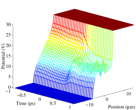
Even prior to photoexcitation of a PCS, the steady-state distribution of extrinsic carriers around the electrodes must be considered in order to determine the complete electric vector-field within the active region of the PCS. In the present study this steady-state space-charge field is automatically calculated (before the optical excitation process is simulated) by iterating the simulation over enough time-steps until an equilibrium electric potential is reached. The form of the screened electric field between the electrodes for an n-type GaAs PCS may be inferred from the gradient of the ps trace in Fig. 6. It can be seen that the extrinsic electron distribution is such that the anode and cathode are screened to similar extents.
Here we focus on the rôle of space-charge screening during and after the arrival of the pump pulse. On photo-excitation electron–hole pairs are generated within the high electric field gap region of a PCS. Charge separation produces a dipole, resulting in the emission of THz radiation. However, the resulting space-charge electric field opposes the applied field, thereby reducing the force experienced by carriers. It is expected that this effect would be particularly significant for carriers photo-injected in the center of the PCS gap at later times.
In Fig. 6 the simulated potential of the PCS is plotted (for ) as a function of -position and time. Before the arrival of the pulse (at 0 ps) the gradient of the potential shows a continuous and positive -component in the region of the gap between the electrodes. After the injection of photo-carriers the potential considerably flattens in the central part of the gap region, corresponding to screening of the electric field.
It can be seen from Fig. 6 that an abrupt change in the potential is present near the edges of the electrodes, which increases as a result of the photo-carrier-induced screening. Therefore, the gradient of the potential will have a large -component, implying a high electric field zone. If the photo-carriers are generated near the electrodes an enhancement of the emitted signal may be expected.
Experimental studies have shown that the power emitted by a PCS may be enhanced by illuminating it asymmetrically. The enhancement is greatest if the region illuminated with the pump-pulse is close to the edge of the anode contactShen et al. (2003); Ralph and Grischkowsky (1991); Keil and Dykaar (1996). This has important practical implications for THz emitter design.
Such “anode-enhanced” THz emission has been explained previously by a trap-enhancement of the electric field near the anode Ralph and Grischkowsky (1991) or by the presence of a high field region near the anode in the case of a Schottky contact Keil et al. (1994). However, experimental measurements Keil and Dykaar (1996) suggest that the asymmetry between two Ohmic electrodes may be attributed to the difference of mobilities between electrons and holes.
As discussed above, the simulation treats the case of PCS electrodes that are each screened to a similar extent before photoexcitation. In reality, depending on the substrate and type of contacts, some asymmetry in this screening may exist. However here we show that the presence of contact asymmetry is not a necessary condition in order to observe “anode-enhanced” THz emission.
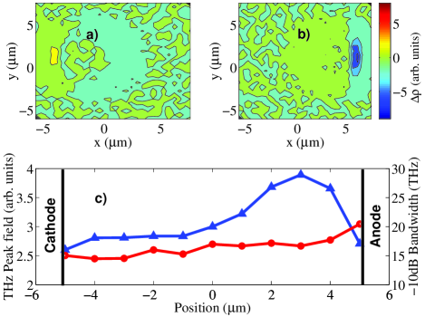
This effect is most easily illustrated by plotting the movement of charge over the duration of the simulation. The contour plots in Fig. 7(a) and (b) show the change in charge density, , as a function of – position of the gap PCS. Plots (a) and (b) are extracted from a simulation where the PCS was illuminated near the cathode and anode respectively. It can be seen that the displaced charge when the PCS is illuminated near the anode is considerable larger.
The enhancement effect can be understood in terms of the higher effective mobility of the photo-injected electron population over the hole population. When photoexcitation occurs close to the anode electrons (holes) migrate into the high (low) field region (see Fig. 6). Therefore, in this case it is the more mobile charges that are affected by the higher electric fields. Thus when electron-hole pairs are generated near the anode the higher electron mobility results in an increase in the effective current density, and as a consequence a larger amplitude THz electric field is emitted.
The above explanation is somewhat simplified, as under typical electric fields inter-valley scattering will lead to a drop in electron mobility. However, as the simulation considers intervalley scattering, all results presented here include this additional effect.
A set of simulations were performed where the laser pulse arrival position was varied across the gap of the PCS. A summary of these data is shown in Fig. 7(c), where the peak electric field is plotted as a function of the distance of the laser pulse from the center of the PCS gap. The peak THz field is enhanced by approximately 40% as the pulse approaches the edge of the anode. The field drops again nearer the anode as a larger fraction of the laser beam-waist is incident outside the active region of the PCS. These results are consistent with previous experimental observations.Shen et al. (2003); Ralph and Grischkowsky (1991); Keil and Dykaar (1996)
The widths of the Fourier transforms at -10 dB of the signal at different positions are also plotted in Fig. 7(c). It is interesting to note that the bandwidth increases as the excitation nears the anode. This can be attributed to the fact that in that region the electric field is greater, resulting in a shorter THz transient, as discussed in Section III.
Finally, it is useful to characterise the timescale of space-charge screening during the photo-excitation of a PCS, so that the influence of pump-pulse duration on the THz emission process can be analysed. We fitted an error function to the position slices of the graph shown in Fig. 6 and chose to define the screening time as 2 standard deviations of that error function. The screening time for this simulation was found to be for all simulated pump pulses between 10 and 100 fs. This suggests that space charge screening is dominated by the intrinsic dynamics of carriers in the semiconductor and it is not significantly affected by the carrier generation time.
VI Conclusions
A semi-classical Monte Carlo model that simulates the carrier dynamics in a photoconductive switch was presented. The THz transient has been shown to narrow with the applied voltage, as well as to be strongly dependent on the pulse width of the exciting laser. The emitted THz power was also studied, and was found to have a maximum for pump pulses of duration. A drop in power for shorter pulses was explained by a broadening in the energy distribution of the exciting pulse, which starts to contain a significant number of photons with sub-band-gap and over L-valley gap energies. This reduces the quantity of free photo-carriers and increases their average effective mass. The reduction in THz power for longer excitation pulses is explained by a decrease in the bias field as a result of screening, since the photo-carriers are injected over a longer period of time.
The screening of the electric bias field was studied. It was found that the screening time is independent of the pump pulses (for pulses under ), implying that the screening time is mainly dependent on the carrier dynamics and not on their injection time on this timescale. The electric field was found to be screened over the gap between the electrodes of the PCS, but not near the edges of the electrodes. This fact combined with the difference of mobilities of electrons and holes produces an increase in the peak THz electric field and a broadening in bandwidth when carriers are photo-excited near the anode edge.
In the future this model promises to be useful for testing new PCS electrode designs and substrate materials (for example low temperature grown GaAs or ion-implanted semiconductors). For better correlation with experimental results it would also be informative to couple a full three-dimensional electromagnetic simulation with the existing carrier dynamics simulation.
VII Acknowledgements
The authors would like to thank the EPSRC (UK) and the Royal Society for financial support of this work, ECC wishes to thank CONACyT (México) for a scholarship.
References
- Huber et al. (2001) R. Huber, F. Tauser, A. Brodschelm, M. Bichler, G. Abstreiter, and A. Leitenstorfer, Nature 414, 286 (2001).
- Leitenstorfer et al. (2002) A. Leitenstorfer, R. Huber, F. Tauser, A. Brodschelm, M. Bichler, and G. Abstreiter, Physica B 314, 248 (2002).
- Kaindl et al. (2003) R. A. Kaindl, D. Hagele, M. A. Carnahan, R. Lovenich, and D. S. Chemla, Phys. Status Solidi B 238, 451 (2003).
- Nuss et al. (1991) M. C. Nuss, K. W. Goossen, J. P. Gordon, P. M. Mankiewich, M. L. Omalley, and M. Bhushan, J. Appl. Phys. 70, 2238 (1991).
- Gao et al. (1995) F. Gao, J. F. Whitaker, Y. Liu, C. Uher, C. E. Platt, and M. V. Klein, Phys. Rev. B 52, 3607 (1995).
- Federici et al. (1992) J. F. Federici, B. I. Greene, P. N. Saeta, D. R. Dykaar, F. Sharifi, and R. C. Dynes, Phys. Rev. B 46, 11153 (1992).
- Han et al. (2000) P. Y. Han, G. C. Cho, and X. C. Zhang, Opt. Lett. 25, 242 (2000).
- Pickwell et al. (2004) E. Pickwell, B. E. Cole, A. J. Fitzgerald, V. P. Wallace, and M. Pepper, Appl. Phys. Lett. 84, 2190 (2004).
- Shen et al. (2003) Y. C. Shen, P. C. Upadhya, E. H. Linfield, H. E. Beere, and A. G. Davies, Appl. Phys. Lett. 83, 3117 (2003).
- Johnston et al. (2002) M. B. Johnston, D. M. Whittaker, A. Corchia, A. G. Davies, and E. H. Linfield, Phys. Rev. B 65, 165301 (2002).
- Shen et al. (2004) Y. C. Shen, P. C. Upadhya, H. E. Beere, E. H. Linfield, A. G. Davies, I. S. Gregory, C. Baker, W. R. Tribe, and M. J. Evans, Appl. Phys. Lett. 85, 164 (2004).
- Ferguson and Zhang (2002) B. Ferguson and X. C. Zhang, Nat. Mater. 1, 26 (2002).
- Shan et al. (2002) J. Shan, A. Nahata, and T. F. Heinz, J. Nonlinear Opt. Phys. Mater. 11, 31 (2002).
- Held et al. (1991) T. Held, T. Kuhn, and G. Mahler, Phys. Rev. B 44, 12873 (1991).
- Auston and Cheung (1985) D. H. Auston and K. P. Cheung, J. Opt. Soc. Am. B 2, 606 (1985).
- Smith et al. (1988) P. R. Smith, D. H. Auston, and M. C. Nuss, IEEE J. Quantum Electron. 24, 255 (1988).
- Rodriguez et al. (1994) G. Rodriguez, S. R. Caceres, and A. J. Taylor, Opt. Lett. 19, 1994 (1994).
- Dekorsy et al. (1993) T. Dekorsy, T. Pfeifer, W. Kutt, and H. Kurz, Phys. Rev. B 47, 3842 (1993).
- Piao et al. (2000) Z. S. Piao, M. Tani, and K. Sakai, Jpn. J. Appl. Phys. Part 1 39, 96 (2000).
- Jepsen et al. (1996) P. U. Jepsen, R. H. Jacobsen, and S. R. Keiding, J. Opt. Soc. Am. B-Opt. Phys. 13, 2424 (1996).
- Liu and Qin (2003a) D. F. Liu and J. Y. Qin, Appl. Opt. 42, 3678 (2003a).
- Nemec et al. (2001) H. Nemec, A. Pashkin, P. Kuzel, M. Khazan, S. Schnull, and I. Wilke, J. Appl. Phys. 90, 1303 (2001).
- Siebert et al. (2004) K. J. Siebert, A. Lisauskas, T. Loffler, and H. G. Roskos, Jpn. J. Appl. Phys. Part 1 43, 1038 (2004).
- Rodriguez and Taylor (1996) G. Rodriguez and A. J. Taylor, Opt. Lett. 21, 1046 (1996).
- Liu and Qin (2003b) D. F. Liu and J. Y. Qin, Int. J. Infrared Millimeter Waves 24, 2127 (2003b).
- (26) J. Lloyd-Hughes, E. Castro-Camus, M. D. Fraser, C. Jagadish, and M. B. Johnston. Phys. Rev. B 70, 235330 (2004).
- Liu et al. (2003) T. A. Liu, M. Tani, and C. L. Pan, J. Appl. Phys. 93, 2996 (2003).
- Shan and Heinz (2004) J. Shan and T. F. Heinz, Top Appl Phys 92, 1 (2004).
- Ralph and Grischkowsky (1991) S. E. Ralph and D. Grischkowsky, Appl. Phys. Lett. 59, 1972 (1991).
- Keil and Dykaar (1996) U. D. Keil and D. R. Dykaar, IEEE J. Quantum Electron. 32, 1664 (1996).
- Keil et al. (1994) U. D. Keil, D. R. Dykaar, R. F. Kopf, and S. B. Darack, Appl. Phys. Lett. 64, 3267 (1994).