Luttinger liquid behavior in weakly disordered quantum wires
Abstract
We have measured the temperature dependence of the conductance in long V-groove quantum wires (QWRs) fabricated in GaAs/AlGaAs heterostructures. Our data is consistent with recent theories developed within the framework of the Luttinger liquid model, in the limit of weakly disordered wires. We show that for the relatively low level of disorder in our QWRs, the value of the interaction parameter , which is the expected value for GaAs. However, samples with a higher level of disorder show conductance with stronger temperature dependence, which does not allow their treatment in the framework of perturbation theory. Fitting such data with perturbation-theory models leads inevitably to wrong (lower) values of .
pacs:
73.21.Hb, 71.10.Pm, 73.23.AdThe electrical conductance through noninteracting clean quantum wires (QWRs) containing a number of one-dimensional subbands is quantized in the universal unit Landauer (1), as observed in narrow constrictions in 2D electron gas (2DEG) systems Wees (2, 3). For such short and clean narrow wires, the e-e interactions described by the so-called Luttinger liquid (LL) model Tomonaga (4) do not affect the value of the conductance, namely it is temperature and length independent as indeed was shown experimentally Wees (2, 3). In the presence of disorder in sufficiently long QWRs, suppression of the conductance is expected at low temperatures. A number of theoretical papers addressing this issue Kane (5, 6, 7, 8) predict a negative correction to the conductance versus temperature , which increases with and obeys a power law: , where is an interaction parameter.
The validity of the implications of the LL theory has been recently demonstrated in a number of experiments Yacoby1 (9, 10). The most evident proofs of the predictions were shown in tunnelling experiments performed in T-shaped cleaved-edged overgrown GaAs quantum wires Yacoby1 (9) and in carbon nanotubes McEuen (10). Earlier non-tunnelling experiments, in which suppression of conductance occurs in the linear response regime, did not unambiguously prove the validity of the theory, and the value of the parameter could not be deduced from the experimental data Tarucha (11, 12, 13). Several complications are encountered in such experiments. For sufficiently disordered wires, where the correction to is expected to be large, the value of the conductance at the plateau is not well defined due to the specific realization of the disordered potential in the wire, as was the case for the long wires of Tarucha et al. Tarucha (11). Moreover, in the intermediate regime, namely for disorder level for which the conductance plateau could be well defined but the corrections to are already significant for a relatively narrow temperature range, cannot be extracted by applying a perturbation theory. If however, the disorder is very weak so that the plateaus are well defined at all temperatures Tarucha (11, 12), the variation of its value versus temperature is so weak that the parameter cannot be reliably determined. Therefore, if one wishes to compare to the theory, a wire possessing just the right amount of disorder is needed.
In this work, we present an experimental study of the conductance in single mode V-groove GaAs QWRs. The variation of conductance was measured over a wide temperature range. Our results are consistent with the theories Maslov1 (7, 8) based on the LL model for weakly disordered wires, allowing us to deduce the value of , as expected for interacting electrons in GaAs and as was observed experimentally in tunneling experiments Yacoby1 (9). We show results for QWRs displaying different amounts of disorder, thus enabling us to show the importance of the degree of disorder and the limits of perturbation theory.
The QWRs studied here were produced by low pressure () metalorganic vapor phase epitaxy (MOVPE) of GaAs/AlGaAs heterostructures on undoped (001) GaAs substrates patterned with V-grooves oriented in the [01-1] direction, fabricated by lithography and wet chemical etching Kapon (14). The heterostructure consisted of a GaAs buffer layer, lower barrier layer, GaAs quantum well (QW) layer, upper barrier layer, and a GaAs cap layer. All layers were nominally undoped, except for two Si doped regions in the barriers, spaced by and , respectively, from the lower and upper GaAs QW interface, serving as modulation doping regions. The layer thicknesses refer to growth on a planar (100) sample. Growth of the GaAs QW in V-grooves yields a crescent-shaped QWR flanked on both sides by {111}A oriented QWs (see inset of Fig. 1). The modulation doping yields a 1D electron gas confined to the wire, laterally connected to 2DEG systems that form on the {111}A QWs.
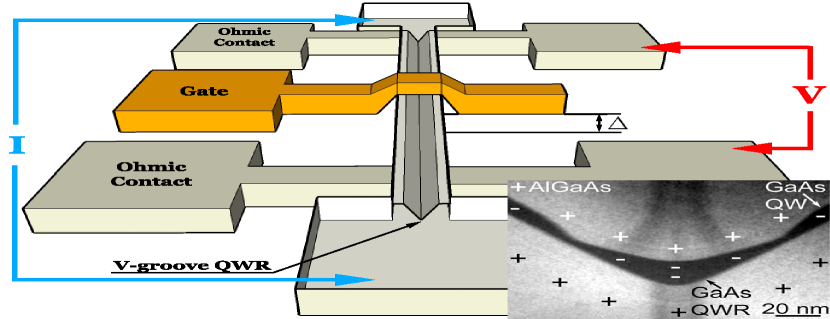
The QWRs were contacted using the scheme illustrated schematically in Fig. 1. Source and drain Au/Ge/Ni pads were fabricated using standard photolithography techniques with a mesa etched along the QWR, providing ohmic contacting to the 2DEG regions. Additionally, narrow () Ti/Au Schottky gates were formed using electron beam lithography in order to isolate the QWR and control the number of populated 1D subbands in it.
The conductance was measured by the four-terminal method using a low noise analog lock-in amplifier (EG&G PR-124A). The excitation current was kept at ensuring that the voltage drop across the wire never exceeded at the lowest temperature. Without application of gate voltage , the transport in our system is carried by electrons in the 2DEG on the sidewalls and in parallel with those in the 1D QWR. Application of a sufficiently large negative depletes the electrons at the sidewalls and creates a 1DEG confined to the V-groove QWR underneath the gate Kaufman1 (15). At a certain range of still more negative voltage, a single populated 1D channel is realized. As was demonstrated Kaufman2 (16), the electrons remain at their one-dimensional state during a transition length (see Fig. 1) on both sides of the gate. This transition length arises from the weak coupling between the 1D states and the located 2DEG, which acts as an electron reservoir. This transition length, defined as the length required for electrons to be scattered into/from the 2DEG, was found to be as large as Kaufman2 (16). It is thus reasonable to conclude that the effective length of the 1D wire exceeds the actual width of the gate ()by about on each side of the gate.
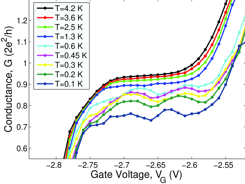
Fig. 2 shows the variation of the conductance with gate voltage , in the range where electrons populate only a single 1D sub-band, at temperatures between and . The temperature was measured using a calibrated carbon thermometer (Matsushita 56 resistor). The electronic temperature of GaAs 2DEG does not deviate from the bath temperature for as shown in our previous studies Shkol (17). The data was taken at stabilized temperatures of the bath while the was swept through the entire range. A series resistance of , measured at , has been subtracted from all curves. At the conductance plateau is smooth with , indicating that only weak disorder is present in our samples. At lower temperatures, some small undulations of the conductance values appear at the plateau, but its average value is well defined with the standard deviation being much less than the average value (see error bars in Figs. 3 and 4). A similar phenomenon, namely the appearance of such structures at lower temperatures and their disappearance at higher temperatures, was also recently observed in clean cleaved-edged overgrown wires Picciotto (18). The variation of the plateau value (approximately ) through the wide temperature range ( decades), allows us to make a meaningful comparison of the data to the theories derived in the appropriate limit of weak disorder. Fig. 3 shows the measured variation of conductance versus temperature.
Early theories, particularly those of Kane and Fisher Kane (5) (and of Ogata and Fukuyama Fukuyama (6)), proposed that for relatively small barriers (weak disorder, which is assumed to result in relatively small corrections), the conductance of a sufficiently long, single mode 1D spinfull Luttinger liquid system decreases with temperature in the manner
| (1) |
Here, is a dimensionless parameter, which is a measure of the strength of the interactions. For repulsive interactions, is given roughly by the expression , where is the Coulomb interaction energy between neighboring electrons. is a parameter describing the strength of the backscattering (disorder) in the wire; at the corrections to become of order . Both theories predict a correction of even for ballistic wires at relatively high temperatures. These imply that for sufficiently long wires, one cannot observe values close to in GaAs, since the value of is expected to be of the order of in such wires, as was already pointed out by Tarucha et al. Tarucha (11).
This contradiction was also addressed in detail in several theoretical papers Maslov1 (7, 8, 19, 20, 21). According to the theory of Maslov Maslov1 (7), the interaction parameter of the wire determines the exponent of the temperature variation, whereas the pre-factor in equation (1) should be set to 1 (noninteracting reservoirs). Fig. 3 (dashed line) shows the curve calculated from this modified equation.
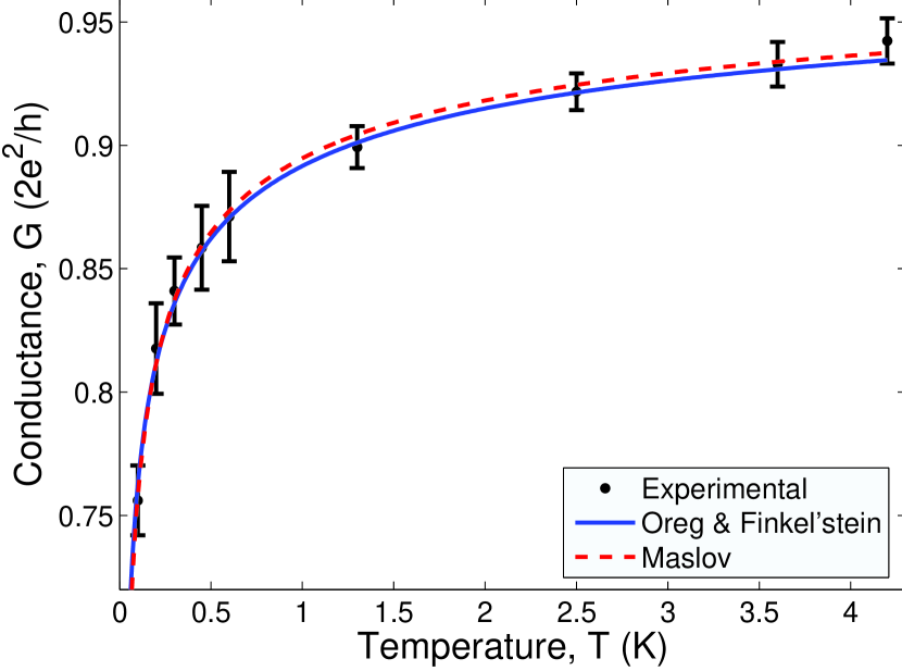
A different but numerically equivalent result was derived by Oreg and Finkel’stein Oreg (8). They also demonstrated that for an infinite clean wire, the conductance keeps the universal value per mode, even in the presence of interactions. According to their theory, because of the electric field renormalization by the interactions, the results given by Kane and Fisher Kane (5) of equation (1) are modified in the following way:
| (2) |
As can be easily verified, the leading term in the temperature variation of the conductance of equation (2) leads to the same results given by Maslov Maslov1 (7).
As one can see from Fig. 3, an excellent fit is obtained for both theories Maslov1 (7, 8), and we obtain , as is expected for electrons in GaAs wires. Indeed, this value is consistent with the experiments in Ref. Yacoby1 (9) , showing values between and . Moreover, using the Fermi energy (half of level spacing between 1D sub-bands estimated in our previous experiments Kaufman1 (15)), we calculate the corresponding electron densities at the middle of the plateau, obtaining . Substituting the above value for into we get which yields the values of , consistent with our fit to the LL model.
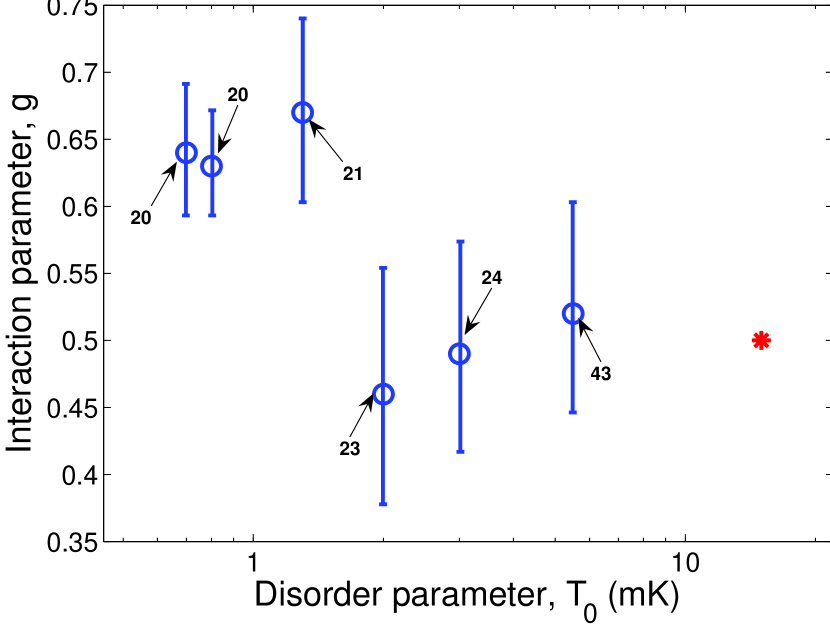
Disorder in V-groove QWRs stems mainly from interface roughness brought about by lithography imperfections on the patterned substrate and peculiar faceting taking place during MOVPE on a nonplanar surface Kapon_a (22). The disorder results in potential fluctuations along the axis of the wire, and manifests itself in localization of excitons and other charge carriers as evidenced in optical spectroscopy studies of these wires Kapon_b (23). Optical and structural studies indicate the formation of localizing potential wells along the wires with size in the range of several Kapon_c (24). The specific features of the disorder in the QWRs studied here, in terms of depth and size of the localization potential, are expected to vary from sample to sample. In fact, the degree of disorder is represented in our analysis of the temperature dependence of the conductance by the parameter . Repeating the analysis of Fig. 3 for several samples, we observed in all the wires having small amount of disorder, namely showing , similar values of , namely . However, other wires with stronger disorder (), showed lower values of g, around . Fig. 4 summarizes the values of g vs. , obtained for our different wires. The values of the total change were calculated for each wire in the temperature range and are also shown in Fig. 4. Note that there is an agreement between the two indicators for the strength of the disorder, and . The transition between and at occurs for . We believe that above the disorder in the wires is strong enough so that the description by perturbation theory is no longer valid. Trying to fit such data with perturbation-theory equations gives inevitably lower (and wrong) values of . For such wires, one should use other theories, concerning stronger disorder due to many impurities Gurnyi (25), or stronger backscattering Fendley (26) in the system. The results of conductance measurements in GaAs wires reported recently by Rother et al. Rother (13) also correspond to highly disordered samples, and also give . Indeed, analyzing their data, we estimate the value of (marked by a star in Fig. 4) and the change in the conductance over a small temperature range (). These values are even larger than corresponding values for our most disordered sample in the same temperature range.
It is highly unlikely that the observed temperature dependence could
be attributed to the contact resistance between the 2DEG and the 1D
subbands outside the gated region for the reasons outlined below:
a) if the contact resistance is treated quantum mechanically Yacoby2 (12),
namely as a change of the transmission from the 2DEG to the 1D
subbands in the ungated region, we would expect that would be similar for any number of 1D channels under the
gate. We however observe that of the
first plateau is much smaller than of
the second plateau at the same temperature range. The latter,
however, is consistent with the expected result of the Luttinger
model when the scattering occurs under the gated region, since the
effect of the Coulomb interaction on the transmission depends on the
number of 1D subbands. Indeed, from an analysis of higher steps in
the conduction depletion curve, used in a smaller temperature range
(, where the plateaux are better resolved), we deduce the
values and for the second and the third plateaux,
respectively, which agrees with the theoretical values of and
Oreg (8).
b) if the decrease of the conductance is considered
as an additional contact resistance added in series to the wire
(i.e., treated classically), than the values of the transmission for
each channel at low temperature at the second plateau would increase
with lowering temperature and eventually exceed unity for each
channel. Therefore, we conclude that the observed decrease of the
conductance is due to the interactions in the LL model.
In conclusion, we have measured the temperature dependence of the electrical conductance in single mode quantum wires. We find that our data is consistent with theoretical calculations Maslov1 (7, 8) based on the LL model, in the limit of weak disorder in the system. We showed that the use of the perturbative result (namely ) in order to estimate , is valid only for wires produced with a moderate amount of disorder ().
We thank Dganit Meidan for constructive discussions of our results. This research was partially supported by the Israel Science Foundation, founded by the Israeli academy Sciences and Humanities Centers of Excellence Program and by ISF grant 845/04.
References
- (1) R. Landauer, IBM J. Res. Develop. 32, 306 (1988).
- (2) B.J. van Wees et al., Phys. Rev. Lett. 60, 848 (1988).
- (3) D.A. Wharam et al., J. Phys. C: Solid State Phys. 21, L209 (1988).
- (4) S. Tomonaga, Prog. Theor. Phys. 5, 544 (1950).
- (5) C.L. Kane, and M.P.A. Fisher, Phys. Rev. B. 46, 15233 (1992).
- (6) M. Ogata, and H. Fukuyama, Phys. Rev. Lett. 73, 468 (1994).
- (7) D.L. Maslov, Phys. Rev. B. 52, R14368 (1995).
- (8) Y. Oreg, and A.M. Finkel’stein, Phys. Rev. B. 54, R14265 (1996).
- (9) O.M. Auslaender et al., Phys. Rev. Lett. 84, 1764 (2000).
- (10) M. Bockrath et al., Nature 397, 598 (1999).
- (11) C. Tarucha et al., Solid State Commun. 94, 413 (1995).
- (12) A. Yacoby et al., Phys. Rev. Lett. 77, 4612 (1996).
- (13) M. Rother et al., Physica E. 6, 551 (2000).
- (14) F. Gustafsson et al., Appl. Phys. Lett. 67, 3673 (1995).
- (15) D. Kaufman et al., Phys. Rev. B. 59, R10433 (1999).
- (16) D. Kaufman et al., Physica E. 7, 756 (2000).
- (17) M. Eshkol et al., Accepted in Phys. Rev. B. (cond-mat/0509285).
- (18) R. de Picciotto et al., Phys. Rev. Lett. 92, 036805 (2004).
- (19) D.L. Maslov, and M. Stone, Phys. Rev. B. 52, R5539 (1995).
- (20) I. Safi, and H.J. Schulz, Phys. Rev. B. 52, R17040 (1995).
- (21) Y. Oreg, and A.M. Finkel’stein, Phys. Rev. Lett. 74, 3668 (1995).
- (22) F. Lelarge et al., J. Crystal Growth. 221, 551 (2000).
- (23) F. Vouilloz et al., Solid State Comm. 108, 945 (1998).
- (24) D.Y. Oberli et al., Phys. Rev. B 59, 2910 (1999); T. Otterburg et al., Phys. Rev. B 71, 033301 (2005).
- (25) I.V. Gornyi et al., Phys. Rev. Lett. 95, 046404 (2005).
- (26) P. Fendley et al., Phys. Rev. B. 52, 8934 (1995).