Planar Hall Effect MRAM
Abstract
We suggest a new type of magnetic random access memory (MRAM) that is based on the phenomenon of the planar Hall effect (PHE) in magnetic films, and we demonstrate this idea with manganite films. The PHE-MRAM is structurally simpler than currently developed MRAM that is based on magnetoresistance tunnel junctions (MTJ), with the tunnel junction structure being replaced by a single layer film.
pacs:
75.47.-m, 75.47.Lx, 75.70.-i, 85.75.DdAmong various technologies considered for future memory applications, magnetic random access memory (MRAM) has attractive properties, since in addition to being nonvolatile with high endurance it can also be as fast as static random access memory (SRAM) and as dense as dynamic random access memory (DRAM).
Storing data in a typical MRAM device is accomplished by applying a magnetic field and causing a magnetic layer in the device to be magnetized in one of two possible states. Reading the data stored in an MRAM device requires reading the electrical resistance of the device, which depends on the magnetization orientation. Currently developed MRAM devices are based on magnetoresistance tunnel junctions (MTJ) tmr1 ; tmr2 , which are comprised of two ferromagnetic layers separated by a thin, electrically insulating, tunnel barrier layer. The operative effect in MTJ structures exploits the asymmetry in the density of states of the majority and minority energy bands in a ferromagnet, with the tunneling resistance depending on the relative orientation of the magnetization vectors in the two magnetic layers. In the parallel configuration, there is a maximal match between the occupied states in one layer and available states in the other layer, leading to a minimum in the tunneling resistance.
Current MTJ structures can achieve percent tmr200percent1 ; tmr200percent2 resistance differences between the parallel and antiparallel magnetization configurations, but these structures require layering of numerous films and relatively precise control of the thickness of the insulating layer. Also, in both states the measured voltage is of the same sign, so if MTJ structures are used in arrays, the variance of the voltages in the array must be much smaller than the difference in the average values of the distribution of the two states in the array.
We suggest here a different approach for storing a magnetic bit, which is based on the planar Hall Effect [PHE] PHE1 . The PHE in magnetic conductors occurs when the resistivity depends on the angle between the current density J and the magnetization M, an effect known as anisotropic magnetoresistance (AMR) amr1 . The AMR yields a transverse electric field when J in not parallel or perpendicular to M. If we assume J in the x direction and M in the x-y plane with an angle between them, the generated electric field has both a longitudinal component:
| (1) |
and a transverse component:
| (2) |
The latter component is denoted the planar Hall effect. Unlike the ordinary and extraordinary Hall effects, the PHE shows an even response upon inversion of J and M. Therefore, the PHE is most noticeable when M changes its axis of orientation, in particular between and . The PHE in magnetic materials has been previously investigated in 3d ferromagnetic metals, such as Fe, Co and Ni films, as a tool to study in-plane magnetization ipm1 . It has also been studied for low-field magnetic sensor applications phs . Recently, large resistance jumps in the PHE have been discovered in the magnetic semiconductor Ga(Mn)As below its Curie temperature, . Four orders of magnitude larger than what has been observed in ferromagnetic metals, it has been termed the giant planar Hall effect (GPHE) gphe1 . We previously reported that the GPHE can be observed in thin manganite films GPHE_LSMO at temperatures up to . Here we show the PHE in manganite films above room temperature. In addition, we demonstrate the possible use of a thin manganite film as a memory cell operating at room temperature.
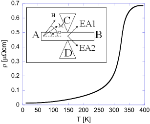
The samples we use are epitaxial thin films ( nm) of (LSMO), with x=0.35, and a resistivity peak temperature of (see Figure 1). The films are patterned for longitudinal and transverse resistivity measurements, with the current path along the [100] and [010] directions. Voltage sensing leads are connected perpendicular to the current path in a ”Hall like” configuration (see inset of Figure 1). The ”active area” (between C and D) on the current path is .
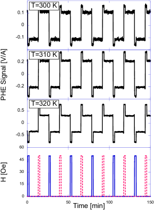
Magnetizing the film along and yields a PHE with opposite signs, according to Eq. 2, which can serve as the two states of a memory cell. Figure 2 shows the PHE signal, , defined as the voltage between C and D divided by the current between A and B, while a field of 50 Oe is applied and then removed along and , at temperatures of 300 K, 310 K, and 320 K. The temperature dependence of the transverse voltage shows that the signal increases with temperature up to T=320 K. In the low temperature regime, the effect is measurable down to T=270 K. We see that the two memory states are clearly separated and stable in time.
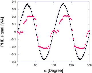
We notice that the PHE signal decreases in absolute value when the field is removed. To explore the origin of this behavior we measured with and without magnetic field as a function of , the angle between the magnetic field and the current (Figure 3). The applied field (50 Oe) is bigger than the coercive field of the sample. Therefore, when the field is on, the magnetization is parallel to the applied field, and follows the behavior expected from Eq. 2. In the absence of the magnetic field, we see that has several plateaus, which we attribute to bi-axial magnetocrystalline anisotropy with easy axes along and , combined with shape anisotropy along the current path. The role of shape anisotropy was revealed by measuring patterns with current paths in different orientations. While the effect of these anisotropies decreases the observed signal, the results presented in Figure 2 indicate that the two magnetic states are still well separated.
The results presented here demonstrate the potential of using the PHE as the basis for a new type of MRAM. The device possesses structural simplicity (a single layer thin film compared to a tunnel junction), and the measured voltages involve a sign reversal between the two states.
L.K. acknowledges support by Intel-Israel and by the Israel Science Foundation founded by the Israel Academy of Sciences and Humanities. L. K. and C. A. acknowledge support from Grant No. 2002384 from the United States - Israel Binational Science Foundation (BSF), Jerusalem, Israel.
References
- (1) J. S. Moodera, Lisa R. Kinder, Terrilyn M. Wong, and R. Meservey, Phys. Rev. Lett. 74, 3273 (1995).
- (2) T. Miyazaki and N. Tezuka, J. Magn. Magn. Mat. 151, 403 (1995).
- (3) C. Goldberg and R. E. Davis, Phys. Rev. 94, 1121 (1954); F. G. West, J. Appl. Phys. 34, 1171 (1963); W. M. Bullis, Phys. Rev. 109, 292 (1958).
- (4) S. S. P. Parkin, C.Kaiser, A. Panchula, P. M. Rice, B. Hughes, M. Samant, S.-H. Yang, Nature Materials 3, 862 (2004)
- (5) S. Yuasa, T. Nagahama, A. Fukushima, Y. Suzuki, K. Ando, Nature Materials, 3, 868 (2004)
- (6) T. R. McGuire and R. I. Potter, IEEE Trans. Magn. 11, 1018 (1975).
- (7) B. Zhao, X. Yan, and A. B. Pakhomov, J. Appl. Phys. 81, 5527 (1997); A. Nemoto, Y. Otani, S. G. Kim, K. Fukamichi, O. Kitakami, and Y. Shimada Appl. Phys. Lett. 74, 4026 (1999); G. Li, T. Yang, Q. Hu, H. Jiang, and W. Lai, Phys. Rev. B 65, 134421 (2002); Z. Q. Lu and G. Pan, Appl. Phys. Lett. 80, 3156 (2002); S. Das, H. Yoshikawa, and S. Nakagawa, J. Appl. Phys. 93, 8098 (2003)
- (8) A. Schuhl, F. Nguyen Van Dau, and J. R. Childress, Appl. Phys. Lett. 66, 2751 (1995).
- (9) H. X. Tang, R. K. Kawakami, D. D. Awschalom, M. L. Roukes, Phys. Rev. Lett. 90, 107201 (2003).
- (10) Y. Bason, L. Klein, J.-B. Yau, X. Hong, C. H. Ahn et al Appl. Phys. Lett.84, 2593 (2004).