Signature of a crossed Andreev reflection effect (CARE)
in the magnetic response of junctions
with the itinerant ferromagnet
Abstract
Magnetic properties of SFS and SF ramp-type junctions with (YBCO) electrodes (S), and the itinerant ferromagnet (SRO - F), were investigated. We looked for a crossed Andreev reflection effect (CARE) in which an electron from one magnetic domain in F is Andreev reflected as a hole into an adjacent, oppositely polarized, domain while a pair is transmitted into S. CARE is possible in SRO since the width of its domain walls is of the order of the YBCO coherence length (2-3 nm). Our junctions behave as typical magnetic tunneling junctions, as the conductance spectra were always asymmetric, and a few showed bound state peaks at finite bias that shifted with field according to the classical Tedrow and Meservey theory. In many of our SFS junctions with a barrier thickness of 10-20 nm, a prominent zero bias conductance peak (ZBCP) has been observed. This peak was found to decrease linearly with magnetic field, as expected for Andreev and CARE scattering. In contrast, in SF junctions, the observed ZBCP was found to decrease versus field almost exponentially, in agreement with the Anderson-Appelbaum theory of scattering by magnetic states in F. Thus, transport in our SFS and SF junctions depends strongly on the size of the F layer. We also found that in both cases, the ZBCP height at zero field decreased with increasing magnetic order of the domains in F, in agreement with the CARE mechanism.
pacs:
74.45.+c, 75.70.-i, 74.50.+r, 74.78.BzProperties of SFS ramp type junctions of
(YBCO) electrodes (S) and (SRO) barrier (F) have been
investigated by two groups more than ten years ago
Char-SRO ; Juelich . Both groups have found that the normal
resistance values of their junctions show two distinct phenomena.
One, that the observed values had a large spread from a few tens
of Ohms to a few hundred Ohms, and the other that they were two or
more orders of magnitude higher than the expected Ohmic resistance
of the SRO film. The high normal resistance was therefore assumed
to originate at the YBCO/SRO interfaces, and more specifically
attributed to oxygen disorder and depletion near the interfaces
Juelich ; Char-interface ; Olsson . Dömel et al.
attributed the high normal resistance to an insulating interface
layer through which quasiparticle tunnelling via localized states
occurred Juelich . A second explanation to the high normal
resistance was given by Antognazza et al. who attributed
it to interface stress created by thermal expansion mismatch in
the junctions Char-SRO . Conductance spectra of YBCO based
SFS junctions with SRO and (CRO) barriers were also
measured by Antognazza et al. Char-conductance .
With both type of barriers they found a zero bias conductance peak
(ZBCP) in the center of a tunneling-like gap structure. The
critical current density however, in the junctions with the CRO
barrier persisted up to a barrier thickness of 50 nm, while that
of the junctions with the SRO barrier vanished abruptly already at
a thickness of 25 nm Char-CRO ; Char-interface . Since SRO is
an itinerant ferromagnet below K Klein ; Zakharov
while CRO is a paramagnet, the different behavior of the critical
current density indicates that the magnetic properties of the
barrier layer play an important role in the transport of these
junctions.
In the present study we revisit the same type of junctions of YBCO
and SRO, with a special focus on transport properties which are
affected by the magnetic nature of the barrier material. In the
absence of a critical current, transport in junctions at voltage
bias values below the energy gap of the superconductor is
controlled by Andreev scattering. When the barrier material is
fully spin polarized in one direction, no Andreev transport is
possible. If however, the ferromagnetic barrier has many domains
with opposite polarizations, a crossed Andreev reflection effect
(CARE) is possible Deutscher . This effect can occur at the
intersection of the domain walls and the YBCO electrodes at the
interfaces, provided the value of the domain walls width is
similar to that of the superconductor’s coherence length
(2-3 nm for optimally doped YBCO). We have chosen to study
junctions with an SRO barrier since the domain wall width of this
highly anisotropic ferromagnet is very narrow (3 nm only
TEM ; Michaelklein ), and fulfils the above condition. As will
be described in the following, our conductance spectra results
under magnetic fields provide supportive evidence for the
existence of CARE in our junctions. It should be noted that
recently CARE was observed by Beckmann et al. in
conventional FSF junctions made of two closely spaced Fe nanowires
in contact with an Al electrode Beckmann . They found that
the resistance difference between parallel and antiparallel
magnetization of the Fe electrodes when the Al electrode was in
the superconducting state, decay with increasing distance of the
Fe electrodes up to about twice the coherence length of Al, in
agreement with the CARE phenomena. Technically however, it is
impossible to reproduced this kind of study in the high
temperature superconductors due to their extremely short coherence
length.
We prepared the YBCO based ramp-type junctions with SRO on (100)
(STO) wafers with a ramp angle of . This
was done by a multi-step process, where the epitaxial thin film
layers are prepared by laser ablation deposition, patterning is
done by deep UV photolithography, and etching by Ar ion milling
Nesher . The YBCO films had c-axis orientation
normal to the wafer. The thickness of the base and cover
electrodes was kept constant at 80 nm, while the SRO thickness on
different wafers ranged between 4 and 80 nm. On each wafer we
patterned ten identical junctions along the (100) direction, with
a width of . Finally, a gold layer was deposited and
patterned to produce the contact pads for the 4-probe
transport measurements. The YBCO electrodes of our junctions had
oxygen content close to optimal doping with a of 88-89 K.
The quality of our junctions fabrication process was tested by
measuring the critical current density of ”shorts”
(junctions without any barrier). We found
which is reasonable compared to
found in the best blanket
films.
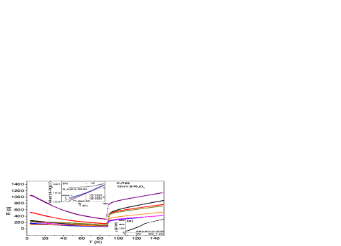
Fig. 1 shows the resistance versus temperature of several junctions
on a single wafer. The spread of resistance values at temperatures
above is extrinsic and due to the different length of
the YBCO leads to the junctions. At low temperatures, the resistance
values have an intrinsic large spread of about one order of
magnitude. These resistance values are also several order of
magnitude higher than the calculated Ohmic resistance
of the junction obtained by using the resistivity of the
film (see inset (a) to Fig. 1). These observations are similar to
the results reported previously on the same kind of junctions by
other groups as discussed in the introduction to this paper
Char-SRO ; Juelich . Unlike previous results however, our
junctions generally had a critical current up to a barrier
thicknesses of nm, but were resistive at higher barrier
thicknesses. Antognazza et al. found critical currents with
a barrier thickness of up to 20 nm Char-SRO . This is
possibly due to microshorts or tunneling via oxygen disorder states
in their junctions. Dömel et al. have found that the
inverse resistance difference of their junctions (where
is the extrapolated resistance to ), varies versus
temperature as . They concluded that this indicates
tunneling via one and two localized states in the barrier
Juelich ; Glazman . We basically observed a similar behavior as
shown in inset (b) to Fig. 1. As one can see however, the results
are very sensitive to and the behavior is not
obtained with the extrapolated , but a value close to it.
Furthermore, in Dömel et al. study, there is no data
between 5-20 K. If we use our data in this temperature range, and
with the extrapolated value, we find a linear
dependence versus T. Thus we believe that tunneling via two
localized states is not the dominant transport mechanism
in our junctions.
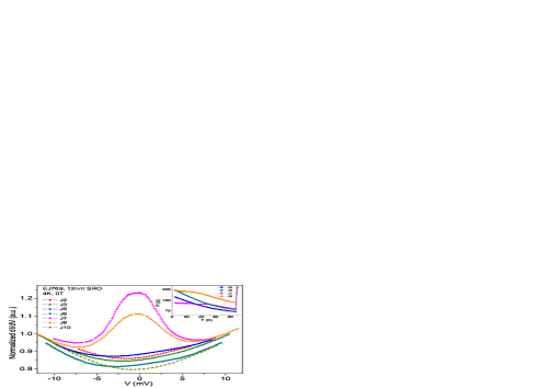
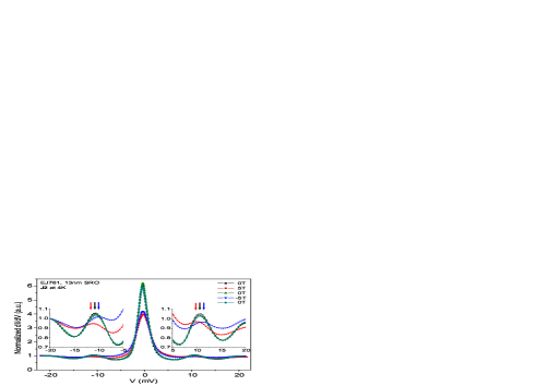
Fig. 2 shows the normalized conductance spectra at low temperature
of several junctions on a single wafer with a barrier thickness of
12 nm. One observes that two junctions have a ZBCP inside a
tunneling-like structure, while the others have only the
tunneling-like behavior. The ZBCP can be attributed to either
Andreev reflections or scattering by magnetic states
Andreev ; Anderson ; Appelbaum . Since our junctions are
orientated along the a or b axes of the YBCO
electrodes, the observed ZBCP is not due to the well known
bound states which are formed along the node direction in a d-wave
superconductor. In addition, we point out that there is a
correlation between the appearance of a ZBCP and the behavior of the
resistance curves below (see the inset to Fig. 2). For
junction J7 and J8, where a ZBCP was observed, the R versus T curves
show a change of slope (a cusp) and not a monotonic increase with
decreasing temperature as for instance is found in junctions J5 and
J6. Another distinct feature in Fig. 2 is that the spectra are
clearly asymmetric. This asymmetry is typical of ferromagnetic
tunneling junctions due to the opposite shifts of the spectra for up
and down spins, and the non zero spin polarization of the magnetic
electrode Tedrow-Meservey . Further support to the fact that
our junctions behave as classical magnetic tunneling junctions, is
found in Fig. 3. In this figure one sees the prominent ZBCP and its
suppression under applied magnetic fields. But first we shall focus
on the bound state peaks observed at about 10 mV. As can be
seen by the zoom up on these parts of the spectra, a positive
magnetic field shifts the peak to negative bias, and vice versa. The
total measured shift for fields of 5 T is 1.2 mV. The
expected shift for an SFS junction is (1.28 mV here)
Tedrow-Meservey . Thus for a bound state of energy ,
the expected shift should be equal to the
measured shift where is the gap energy.
Therefore, and if of YBCO is
20 meV then 10 meV, in agreement with
the peaks bias of the bound state in Fig. 2.
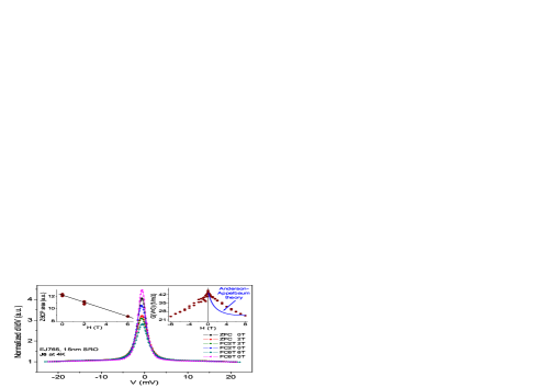
Fig. 4 shows a few conductance spectra under different fields and
field cooling conditions. There is almost no effect on the spectra
at any given field larger than about 0.1T, whether it was obtained
under zero field cooling (ZFC) or field cooling (FC). The insets
of Fig. 4 show the ZBCP area above the background conductance, and
the conductance at zero bias () versus
field. Surprisingly, both features show a linear decrease
with increasing field, except maybe for fields near zero field.
The expected decrease of versus field due to scattering by
magnetic states in junctions was calculated by Appelbaum and found
to be almost exponential Appelbaum67 . A similar behavior,
but with a more gradual decrease versus field, was found also in
experiments done in Ta-I-Al tunnel junctions
Appelbaum-Shen . Thus the linear versus result in
our junctions points to a different scattering mechanism. A
theoretical calculation of the current and magnetoresistance in
FSF junctions due to CARE was recently published, but it did not
include conductance spectra which are relevant in the present
study Yamashita . The closest theoretical calculation we
could find for a ZBCP behavior versus was in a study by Tanaka
et al. Tanaka . They calculated the conductance
spectra for the node direction in the cuprates using the extended
BTK model for the d-wave superconductors. Clearly, the resulting
ZBCP is due to bound states because of the sign change of the
order parameter, and not to the CARE process. Nevertheless, the
basic scattering mechanism is still Andreev reflections, and
therefore a comparison of our data with their results is
justified. Extracting from their conductance spectra at
different fields, one finds a clear linear decrease with field.
Hence, our data is consistent with this behavior, and it is likely
that simple Andreev and CARE play a dominant role in the transport
of our SFS junctions.
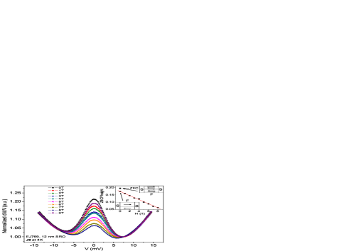
Fig. 5 shows a series of conductance spectra in another junction.
These spectra were obtained under various fields starting with ZFC
to 4 K, ramping up to 8 T, and going back to zero field. Here
again as in Fig. 4, one finds a linear decrease of the ZBCP height
versus field as shown in the inset to this figure, but the ZFC data
point seems to stand out. Clearly the measured ZBCP height after ZFC
is larger than that obtained after field cycling to 8 T and back to
0 T. To understand this behavior, we note that during the ZFC
process, the SRO barrier layer becomes ferromagnetic with many
domains and domain walls as shown schematically in the upper-right
corner of the inset. As a result, the contribution of CARE to the
conductance which depends on the number of domain wall intersections
with the S electrodes, should be higher than the conductance after
field cycling. This is so since the magnetic memory after the field
cycling reduces the number of domains as shown schematically in the
lower-left corner of the inset to Fig. 5. Because this is exactly
the observed result, we conclude that CARE is responsible for the
excess conductance at zero field under ZFC as shown in the inset to
Fig. 5. We stress that this phenomenon is a unique signature of
CARE, which can not
be explained by the standard Andreev reflections.
Next, we decided to look at the limit of a very thick barrier. Since
the Ohmic resistivity of SRO is quite small at 4 K, only as shown in inset (a) of Fig. 1, we chose to study
SF rather than SFS junctions. In this case, the F electrode
”thickness” or size is almost infinite, and therefore its relatively
weak itinerant ferromagnetism should be enhanced Klein . The
resulting conductance spectra of a typical SF junction are shown in
Fig. 6. The spectra and the ZBCP height values versus field were
obtained by ZFC to 4 K, ramping to 6 T, and going back to 0 T.
The ZBCP inside a gap-like structure is still present, but its
magnitude is greatly reduced compared to the previous data in SFS
junctions. The interesting feature here is that already at 4 T, the
ZBCP is almost fully suppressed. Even more amazing is the field
dependence of the ZBCP height as shown in the inset to Fig. 6. This
is clearly nonlinear, and rather close to exponential
decay. Actually, this decay is very similar to that predicted by the
Anderson-Appelbaum (AA) theory of scattering by magnetic states
close to the interface with a superconductor
Anderson ; Appelbaum ; Appelbaum-Shen . It should be noted that in
the AA model this decay is due to the increased Zeeman splitting of
the ZBCP Appelbaum67 . We however, have never observed
splitting of the ZBCP, and this could be due to a larger magnetic
relaxation rate in SRO which broadens this peak and smears the
splitting. It is therefore concluded that the almost exponential
decay versus field indicates that the dominant transport mechanism
now is not Andreev scattering, but rather magnetic scattering. We
conclude that the size of the F electrode plays an important role in
determining the transport properties of our junctions. When the F
electrode is thin as in the previous results of SFS junctions
(10-20 nm), its ferromagnetism is weak and the proximity effect by
the S electrodes makes it even weaker. The opposite is true when the
F electrode size is large as in the SF junctions case. Then the
proximity penetration of superconductivity into F is small compared
to the mean free path in the F electrode (which is unlimited now by
the junction length), the ferromagnetic order in F is robust, and
the transport in the junction is controlled
mostly by magnetic scattering.
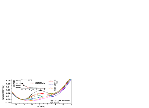
We note that the value of the ZBCP height after ZFC from room
temperature to 4 K is still much larger than its value after field
cycling to 6 T and back to 0 T, similar to the result in the SFS
junction of Fig. 5. It is tempting to attribute this behavior to
CARE as before, but then the absence of a linear decreasing
component of the ZBCP height versus field which originates in
Andreev scattering, will have to be explained. According to Yokoyama
et al. who calculated the conductance spectra due to
magnetic scattering in SN junctions with a d-wave superconductor
Tanaka3 , an enhanced magnetic scattering rate (by the higher
magnetic disorder after ZFC in the present study) would decrease
rather than increase the ZBCP. Since this is opposite to
observation, it seems that we are still dealing with suppression of
the ZBCP height due to CARE here (from the magnetically disordered
ZFC state to the more ordered state after field cycling, similar to
the result in Fig. 5). Apparently, in the SF case where the
ferromagnetism of F is robust, the linear suppression of the ZBCP
height versus field is much enhanced and terminates at a much
smaller applied field. This leaves only the exponential decay versus
field due to magnetic scattering as the
dominant process.
In conclusion, we have found significant magnetic effects in the
transport properties of SFS and SF junctions of YBCO and the SRO
ferromagnet. i) We observed an asymmetry in the
conductance spectra, and shifts of bound state peaks with field,
which are typical of magnetic tunneling junctions. ii) In
both type of junctions a prominent ZBCP was observed. Its height
decreased linearly with increasing field in SFS junctions, but
almost exponentially in the SF case. The ZBCP height dependence on
originated in normal Andreev and CARE in the SFS junctions,
but was dominated by magnetic scattering in the SF junctions.
iii) The observation of a higher ZBCP height at 0 T
after ZFC as compared to the value after field cycling is due to
the higher magnetic disorder after ZFC in both SFS and SF
junctions. This is a strong signature of a CARE phenomenon in our
junctions. Finally, we note that a calculation of the conductance
spectra under fields in SF and SFS junctions is needed for a more
quantitative comparison with the present results.
Acknowledgments: The authors are grateful to G. Deutscher,
L. Klein, O. Millo and E. Polturak for useful discussions. This
research was supported in part by the Israel Science Foundation
(grant # 1564/04), the Heinrich Hertz Minerva Center for HTSC,
the Karl Stoll Chair in advanced materials, and by the Fund for
the Promotion of Research at the Technion.
References
- (1) L. Antognazza, K. Char, T.H. Geballe, L. L. King, and A.W. Sleight, Appl. Phys. Lett. 63, 1005 (1993).
- (2) R. Domel, C. Horstmann, M. Siegel, A. I. Braginski, and M. Yu. Kupriyanov, Appl. Phys. Lett. 67, 1775 (1995).
- (3) K. Char, L. Antognazza, and T.H. Geballe, Appl. Phys. Lett. 63, 2420 (1993).
- (4) E. Olsson, K. Char, Appl. Phys. Lett. 64, 1292 (1994).
- (5) L. Antognazza, K. Char, and T.H. Geballe, Appl. Phys. Lett. 68, 1009 (1996).
- (6) K. Char, M. S. Colclough, T.H. Geballe, and K. E. Myers, Appl. Phys. Lett. 62, 196 (1993).
- (7) L. Klein, J. S. Dodge, C. H. Ahn, J. W. Reiner, L. Mieville, T. H. Geballe, M. R. Beasley and A. Kapitulnik, J. Phys.: Condens.Matter 8, 10111 (1996).
- (8) N. D. Zaharov, K. M. Satyalakshmi, G. Koren, D. Hesse, J. Mater. Res. 14, 4385 (1999).
- (9) G. Deutscher, D. Feinberg, Appl. Phys. Lett. 76, 487 (2000).
- (10) A. F. Marshall, L. Klein, J. S. Dodge, C. H. Ahn, J. W. Reiner, L. Mieville, L. Antagonazza, A. Kapitulnik, T. H. Geballe, and M. R. Beasley, J. Appl. Phys. 85, 4131 (1999).
- (11) M. Feigenson, L. Klein, J. W. Reiner, and M. R. Beasley Phys. Rev. B 67, 134436 (2003).
- (12) D. Beckmann, H. B. Weber, and H. v. Löhneysen, Phys. Rev. Lett. 93, 197003 (2004).
- (13) O. Nesher and G. Koren, Appl. Phys. Lett. 74, 3392 (1999).
- (14) L.I.Glazman and K.A.Matveev, Sov. Phys. JETP 67, 1276 (1988) [Zh. Eksp. Teor. Fiz. 94, 332 (1988)].
- (15) A. F. Andreev, Sov. Phys. JETP 19, 1228 (1964) [Zh. Eksp. Teor. Fiz. 46, 1823 (1964)].
- (16) J. Appelbaum, Phys. Rew. Lett. 17, 91 (1966).
- (17) P. W. Anderson, Phys. Rew. Lett. 17, 95 (1966).
- (18) P.M. Tedrow, R. Meservey, Phys. Rev. B 7, 318 (1973).
- (19) J. A. Appelbaum, Phys. Rev. 154, 633 (1967).
- (20) J. A. Appelbaum, L. Y. L. Shen, Phys. Rev. B 5, 544 (1972)
- (21) T. Yamashita, S. Takahashi, and S. Maekawa, Phys. Rev. B 68, 174504 (2003).
- (22) Y. Tanaka, H. Itoh, H. Tsuchiura, Y. Tanuma, J. Inoue and S. Kashiwaya, Physica C. 367, 73 (2002).
- (23) T. Yokoyama, Y. Tanaka, A. A. Golubov, J. Inoue and Y. Asano, Phys. Rev. B 71, 094506 (2005).