Chapter 2 Charge Tunneling Rates in Ultrasmall Junctions
Charge Tunneling Rates in Ultrasmall Junctions GERT-LUDWIG INGOLD
Fachbereich Physik, Universität-GH Essen, 4300 Essen, Germany
and
YU. V. NAZAROV
Nuclear Physics Institute, Moscow State University, Moscow 119899 GSP, USSR
1. Introduction
1.1. Ultrasmall tunnel junctions
With the advances of microfabrication techniques in recent years it has become possible to fabricate tunnel junctions of increasingly smaller dimensions and thereby decreasing capacitance . Nowadays one can study tunnel junctions in a regime where the charging energy is larger than the thermal energy . Then charging effects play an important role and this has been the subject of a by now large body of both theoretical and experimental work.
To study ultrasmall tunnel junctions, that is tunnel junctions with capacitances of F or less, one may either use metal-insulator-metal tunnel junctions or constrictions in a two-dimensional electron gas formed by a semiconductor heterostructure. Due to the very different density of charge carriers in metals and semiconductors the physics of metallic tunnel junctions and two-dimensional electron gases with constrictions differ. In this chapter we restrict ourselves to metallic tunnel junctions while Chap. 5 is devoted to single charging effects in semiconductor nanostructures.
Metal-insulator-metal tunnel junctions produced by nanolithography are widely studied today. Other systems where metallic tunnel junctions are present include granular films, small metal particles embedded in oxide layers, crossed wires, and the scanning tunneling microscope. The general setup consists of two pieces of metal separated by a thin insulating barrier as shown in Fig. 1.

The metal may either be normal or superconducting at low temperatures. In the latter case, one may study Josephson junctions with ultrasmall capacitances as well as normal tunnel junctions if a sufficiently high magnetic field is applied.
Classically, there is no electrical transport through the barrier and the junction will act like a capacitor of capacitance . By connecting a single junction to an external circuit it may be charged with a charge where is the voltage applied to the junction. The charge is an influence charge created by shifting the electrons in the two metal electrodes with respect to the positive background charge. A very small shift of the electrons will lead to a small change in . Therefore, the charge is continuous even on the scale of the elementary charge. One finds that for such small charges the interaction between the two charge distributions on either side of the barrier may still be described by a charging energy .
Taking into account quantum effects there is a possibility of charge transport through the barrier by tunneling of electrons indicated by the arrows in Fig. 1. In contrast to the charge motion in the electrodes this transport process involves discrete charges since only electrons as an entity may tunnel. The typical change in energy for such a process is therefore the charging energy .
This energy scale has to be compared with the other energy scale present in the system, namely . Since our interest is in the discussion of charging effects we require . Otherwise thermal fluctuations will mask these effects. As an example let us note that a junction with an area of about and a typical oxide layer thickness of 10Å has a capacitance of about corresponding to a temperature of about . For decreasing capacitance which requires decreasing dimensions of the junction this restriction for temperature becomes more relaxed.
1.2. Voltage-biased tunnel junction
In the following two sections we present two different pictures for the behavior of tunnel junctions. We will not give very detailed derivations at this point since similar calculations will be presented in subsequent sections.
Let us first consider a tunnel junction coupled to an ideal voltage source . In order to determine the current-voltage characteristic one needs to calculate electron tunneling rates in both directions through the junction taking into account the external bias. The tunneling process is described by a tunneling Hamiltonian [1]
| (1) |
where the term written out explicitly describes the annihilation of an electron with wave vector and spin on the left electrode and the creation of an electron with the same spin but wave vector on the right electrode thereby transferring an electron from the left to the right side. The corresponding matrix element is given by . The Hermitian conjugate part describes the reverse process. We note that what we call electrons here for simplicity, are really quasiparticles of the many-electron system in the electrodes.
As a result of a golden rule calculation treating as a perturbation and assuming an elastic tunneling process one finds after some calculation for the average current
| (2) |
Here, is the Fermi function at inverse temperature . The integrand of (2) can easily be understood. The first term gives the probability to find an electron with energy on the left side and a corresponding empty state on the right side. The difference in the Fermi energies on both sides of the barrier is accounted for in the argument of the second Fermi function. This difference is assumed to be fixed to by the ideal voltage source. An analogous interpretation may be given for the second term in the integrand which describes the reverse process. The tunneling matrix element and the densities of state were absorbed in which is proportional to . The integral in (2) will be calculated explicitly in Sec. 3.2. where we will find independent of temperature
| (3) |
Since this gives a current proportional to the applied voltage, the current-voltage characteristic is of the same form as for an Ohmic resistor. It is therefore suggestive to call a tunneling resistance. We stress, however, that the tunneling resistance should not be confused with an Ohmic resistance because of the quite different nature of charge transport through a tunnel junction and an Ohmic resistor. This becomes apparent for example in the different noise spectra.[2]
1.3. Charging energy considerations
In the previous section we have discussed a tunnel junction coupled to an ideal voltage source. As a consequence, the charge on the junction capacitor is kept fixed at all times. Now, we consider a different case where an ideal external current controls the charge on the junction. At zero temperature a tunneling process leading from to is only possible if the difference of charging energies before and after the tunneling process is positive
| (4) |
This condition is satisfied if or the voltage across the junction . Note, that we distinguish between the voltage across the junction and an externally applied voltage .
Assuming an ideal current-biased junction, the following picture results. Starting at a charge , the junction is charged by the external current. At a charge an electron may tunnel thereby decreasing the charge on the junction below the threshold . Then the cycle starts again. This process which occurs with a frequency only determined by the external bias current is called SET oscillation.[3]–[5] One can show that the average voltage across the junction is proportional to .
We may also use an ideal voltage source and feed a current to the junction through a large resistor. Its resistance is assumed to be smaller than the tunneling resistance of the junction but large enough to inhibit a fast recharging of the capacitor after a tunneling event. According to the argument given above there will be no current if the external voltage is smaller than . Beyond this voltage one finds at zero temperature that the average current is determined by an Ohmic current-voltage characteristic with resistance shifted in voltage by . This shift in the current-voltage characteristic is called the Coulomb gap and the phenomenon of suppression of the current below is referred to as Coulomb blockade. For the energy consideration presented in this section it was important that the charge on the capacitor is well defined and continuous even on the scale of an elementary charge. Only a junction charge less than together with the fact that tunneling always changes this charge by gave rise to the possibility of a Coulomb gap.
1.4. Local and global view of a single tunnel junction
Comparing the discussions in the two previous sections we find that there are different energy differences associated with the tunneling process, namely and . As we will argue now these two cases can be viewed as a local and a global description [4]–[6] of a single tunnel junction coupled to an external circuit, at least at zero temperature. In Sec. 1.3. we used the energy difference (4) which gives the difference in charging energy of the junction before and immediately after the tunneling process. This is called the local view since it only considers the junction through which the electron is tunneling and ignores its interaction with the rest of the world.
In contrast, in Sec. 1.2. the energy changes in the circuit were viewed globally. After the tunneling process a nonequilibrium situation occurs since the charge on the junction and the charge imposed by the voltage source are different. To reestablish equilibrium the voltage source transfers an electron and recharges the junction capacitor to the charge . In the end there is no change in charging energy. However, the work done by the voltage source which amounts to has to be taken into account. This is indeed the case in (2) where appears as the difference between the Fermi energies of the two electrodes.
Now, the question arises which one of these two descriptions, if any, is correct. This problem cannot be solved by treating the single junction as decoupled from the rest of the world or by replacing its surroundings by ideal current or voltage sources. The discussion of the local and global view rather suggests that one has to consider the junction embedded in the electrical circuit.[7]–[9] A junction coupled to an ideal voltage source, for example, will always behave according to the global rule since after the tunneling process charge equilibrium is reestablished immediately. This is not the case if the voltage source is attached to the junction with a large resistor in series. In the sequel we will discuss the influence of the electrodynamic environment on electron tunneling rates in ultrasmall tunnel junctions. We will learn that the local and global rules are just limiting cases of the so-called orthodox theory and find out to what kind of circuit we have to couple the junction in order to observe Coulomb blockade phenomena.
2. Description of the environment
2.1. Classical charge relaxation
In this section we discuss the coupling of a tunnel junction to the external circuit classically. That means that we forget about tunneling for the moment and consider the junction just as a capacitor of capacitance carrying the charge where is the voltage across the junction. The junction is attached to the external circuit which we describe by its impedance
| (5) |
The impedance gives the ratio between an alternating voltage of frequency applied to the circuit and the current which then is flowing through it if the junction capacitor is replaced by a short. The external circuit shall contain an ideal dc voltage source in series with the impedance as shown in Fig. 2.

As discussed in Chap. 1 and [8, 10], the assumption of a voltage source is reasonable even if in a real experiment a current source is used. Generally, the leads attached to the junction generate a capacitance which is so large compared to the junction capacitance that a current source will charge this large capacitor which then acts as an effective voltage source.
In equilibrium the average charge on the junction is determined by the external voltage source. Let us assume now that at some initial time the equilibrium is disturbed and the charge on the junction is . In the following we will derive the relaxation from this initial condition back to equilibrium. The information on the charge relaxation which depends only on the external impedance and the junction capacitance will later be needed to describe the influence of the environment.
To solve this initial value problem it is convenient to work in the Laplace space. Then the Laplace transform of the voltage across the impedance follows from (5) as
| (6) |
where the hat denotes the Laplace transform and
| (7) |
Applying the rule for the Laplace transformation of a derivative, one finds for the current in terms of the charge
| (8) |
Since the Laplace transform of the constant external voltage is , we get for the voltage balance in the circuit
| (9) |
Solving this equation for , doing the inverse Laplace transformation, and rewriting the final result in terms of the original impedance we get for the relaxation of the charge
| (10) |
Here, the Fourier transform of the charge relaxation function
| (11) |
is related to the total impedance
| (12) |
of the circuit consisting of the capacitance in parallel with the external impedance . It will become clear in Sec. 6.2. that is the effective impedance of the circuit as seen from the tunnel junction.
2.2. Quantum mechanics of an -circuit
In the previous section we have found that the classical relaxation of charge in a circuit can be described in terms of its impedance. We will now make a first step towards the quantum mechanical treatment of a tunnel junction coupled to an external circuit by discussing the most simplest case where the environmental impedance of the circuit shown in Fig. 2 is given by an inductance . In the next section this will turn out to be the fundamental building block for a general description of the environment.
For the following it is convenient to introduce the phase [11]
| (13) |
where is the voltage across the junction. The definition (13) becomes the Josephson relation for a superconducting tunnel junction if we replace the electron charge by the charge of Cooper pairs . In the superconducting case this phase is of course of great importance as the phase of the order parameter.
To derive the Hamiltonian of a voltage-biased -circuit let us first write down the Lagrangian
| (14) |
The first term represents the charging energy of the capacitor which can easily be verified by means of the definition of the phase (13). The magnetic field energy of the inductor is given by the second term since up to a factor the flux through the inductor is given by the phase difference across the inductor. The latter relation is obtained from the requirement that the phase differences at the capacitor and inductor should add up to the phase difference produced by the voltage source according to (13).
Switching to the Hamilton formalism we find that the charge on the junction is the conjugate variable to . In a quantum mechanical description this results in the commutation relation
| (15) |
Now, the phase , the voltage across the junction, and the charge are operators. Note that there is no problem with phase periodicity when constructing the phase operator . Due to the continuous charge the spectrum of the phase operator is continuous on the interval from to .
From the Lagrangian (14) we immediately get the Hamiltonian
| (16) |
According to the equations of motion derived either from (14) or (16) one finds that the average phase evolves in time like . The average charge on the capacitor is given by . It is therefore convenient to introduce the variables
| (17) |
and
| (18) |
describing the fluctuations around the mean value determined by the external voltage. The commutator between the new variables is again
| (19) |
Substituting by in the Hamiltonian (16) amounts to going into a “rotating reference frame”. This transformation results in an extra contribution to the time derivative in the time-dependent Schrödinger equation. We thus obtain, up to a term depending only on the external voltage,
| (20) |
which demonstrates the equivalence between an -circuit and a harmonic oscillator. Note that the influence of an external voltage is entirely accounted for by the definitions (17) and (18).
2.3. Hamiltonian of the environment
The special environment of the previous section did not give rise to dissipation so that there were no problems in writing down a Hamiltonian. On the other hand, in general, an impedance will introduce dissipation. At first sight, this is in contradiction to a Hamiltonian description of the environment. However, after realizing that dissipation arises from the coupling of the degrees of freedom and , in which we are interested, to other degrees of freedom our task is not as hopeless anymore. We will introduce a Hamiltonian for the system coupled to the environment which, after elimination of the environmental degrees of freedom, describes a dissipative system. One approach would be to start from a microscopic model. This will be discussed in the appendix. Here, we represent the environment by a set of harmonic oscillators which are bilinearly coupled to and which may be viewed as -circuits. These harmonic oscillators may in some cases be justified microscopically. In most cases, however, this representation of the environment is introduced phenomenologically. It then has to fulfill the requirement that in the classical limit the reduced dynamics is described correctly. We now can write down the Hamiltonian for the environmental coupling
| (21) |
which is expressed in terms of the variables and defined in (17) and (18) thereby accounting for an external voltage source. The first term describes the charging energy of the junction capacitor. In the second term we sum over the environmental degrees of freedom represented by harmonic oscillators of frequency which are bilinearly coupled to the phase of the tunnel junction. In order to describe an effectively dissipative environment the number of environmental degrees of freedom has to be rather large. Usually, in practice the limit has to be performed. The model Hamiltonian (21) is not new. Hamiltonians of this form have been used in quantum optics for several decades.[12] More recently, Caldeira and Leggett [13] introduced this description of the environment in the context of macroscopic quantum tunneling.
To derive the reduced dynamics of the system described by (21) we write down the Heisenberg equations of motion for the operators and . It is easy to solve for and by considering as a given function of time. After substituting the result into the equations of motion for and and solving these we obtain after a partial integration
| (22) |
Here,
| (23) |
Note that an arbitrary function can be described in this way by an adequate choice of the model parameters and . In general, for a given the sum has to be replaced by an integral over a continuous distribution of harmonic oscillators. The Fourier transform of is the admittance . The inhomogeneity in (22) is the quantum mechanical noise current and depends on the initial conditions at . By Laplace transforming the left-hand side of (22) we recover (9) which describes the classical relaxation of the junction charge according to the total impedance introduced in (12). Therefore, the Hamiltonian (21) gives us an equivalent description of the environment which enables us to treat a tunnel junction coupled to the external circuit quantum mechanically.
Sometimes it is useful to use a mechanical analogue of the model presented above. The correspondence between the electrical and mechanical quantities is given in table I.
| Electrical quantity | Mechanical quantity |
|---|---|
| charge | momentum |
| voltage | velocity |
| capacitance | mass |
| phase | coordinate |
| inductance | spring constant |
| -circuit | harmonic oscillator |
3. Electron tunneling rates for single tunnel junctions
3.1. Tunneling Hamiltonian
In the previous section we have treated the tunnel junction as a capacitor thereby neglecting the fact that electrons may tunnel through the junction. We will now include tunneling to allow for a current through the junction. The quasiparticles in the two metal electrodes are described by the Hamiltonian
| (24) |
where the first and second sum correspond to the left and right electrode, respectively. and are the energies of quasiparticles with wave vector and while denotes their spin.
Tunneling is introduced by the Hamiltonian [8, 14, 15]
| (25) |
This is the tunneling Hamiltonian (1) presented in Sec. 1.2. apart from the operator . Using the mechanical analogue of Sec. 2.3. the latter operator would correspond to a momentum shift operator. Indeed according to
| (26) |
which follows from the commutator (15) this new operator acts as a “translation” operator changing the charge on the junction by an elementary charge . In the Hamiltonian (25) we use operators and representing quasiparticles and in addition the phase which is conjugate to the charge . These operators may be expressed in terms of true electron creation and annihilation operators. In the following, we will assume that the quasiparticle operators commute with the charge and phase operators since a large number of quasiparticle states contribute to these operators and the contribution of a single state is negligible. This is closely related to the assumption of linearity of the electrodynamics in the system under consideration. Although quasiparticle and charge operators commute, the tunneling Hamiltonian (25) now establishes a coupling between the tunneling electron and the environment which “sees” the junction charge. It will be shown below that this coupling makes the current-voltage characteristic of the junction nonlinear.
As in Sec. 2.2. we may introduce the phase defined in (17) into . This will help to clarify the relation between the two tunneling Hamiltonians (1) and (25). Exploiting the relation
| (27) |
we perform a time-dependent unitary transformation with
| (28) |
The new tunneling Hamiltonian then reads
| (29) |
Since the transformation (28) is time-dependent is also shifts quasiparticle energies on the left electrode and we obtain from (24)
| (30) | |||||
In the absence of an environment, the operator in (29) has no effect on the tunneling process. The Hamiltonian (29) then becomes identical to the Hamiltonian (1). The phase factor which was present in (25) has vanished. Instead, the energy levels on the left and right electrodes are shifted by relative to each other. This shift was taken into account in the result (2).
In the following we will use the tunneling Hamiltonian in the form (29). Before starting with the calculation let us collect the Hamiltonians describing the whole system. The total Hamiltonian
| (31) |
contains the contributions of the quasiparticle Hamiltonian (30) for the two electrodes, the Hamiltonian (21) describing the environment including the charge degree of freedom, and finally the tunneling Hamiltonian (29) which couples the first two parts.
3.2. Calculation of tunneling rates
3.2.1. Perturbation theory
Starting from the Hamiltonian (31) we now calculate rates for tunneling through the junction. First we make two important assumptions. The tunneling resistance shall be large compared to the resistance quantum which is a natural resistance scale (for Josephson junctions one often uses to account for the charge of Cooper pairs). Since is inversely proportional to the square of the tunneling matrix element, this implies that the states on the two electrodes only mix very weakly so that the Hamiltonian (30) is a good description of the quasiparticles in the electrodes. We then may consider the tunneling Hamiltonian as a perturbation. Here, we will restrict ourselves to the leading order, i.e. we calculate the tunneling rate within the golden rule approximation. We further assume that charge equilibrium is established before a tunneling event occurs. This defines the states to be used in the perturbation theoretical calculation as equilibrium states. On the other hand, it means that the time between two tunneling processes should be larger than the charge relaxation time.
As mentioned above we will calculate the tunneling rates by means of the golden rule
| (32) |
which gives the rate for transitions between the initial state and the final state . In the absence of the tunneling Hamiltonian we may write the total state as a product of a quasiparticle state and a charge state which in the following we call reservoir state because it is connected with the coupling to the environment. Specifically, we set and where and are quasiparticle states of respective energy and and are reservoir states with energies and . The matrix element in (32) then becomes
| (33) |
with
| (34) |
being the part of the tunneling Hamiltonian acting in the quasiparticle space.
To calculate the total rate for electron tunneling from left to right we have to sum over all initial states weighted with the probability to find these states and over all final states. We thus have to evaluate
| (35) | |||||
Let us consider one term contained in . The only possible states with nonvanishing matrix element are and where this notation means that in a quasiparticle with wave vector and spin on the left side of the barrier is present while the state with wave vector and spin on the right side is unoccupied. The occupation of states with other quantum numbers is arbitrary. Since factorizes we then obtain
| (36) | |||||
Here, the probability to find the initial state is given by the product of Fermi functions and is the difference of quasiparticle energies associated with the tunneling process since the occupation of the other states remains unchanged. Note that does not appear in since the Fermi level on the left side is shifted by this amount. If the applied voltage is such that is much smaller than the Fermi energy we may assume that all quasiparticle states involved have energies close to the Fermi energy. Taking the tunneling matrix element to be approximately independent of and we may replace by an averaged matrix element which also accounts for the density of states at the Fermi energy. We collect all constant terms in the tunneling resistance . The rate expression (36) then becomes
| (37) | |||||
where we have renamed the energies and into and . The justification for calling a tunneling resistance will be given below when we calculate current-voltage characteristics.
3.2.2. Tracing out environmental states
We now have to do the sum over and in (37). The probability of finding the initial reservoir state is given by the corresponding matrix element
| (38) |
of the equilibrium density matrix
| (39) |
of the reservoir at inverse temperature . Here,
| (40) |
is the partition function of the environment. To proceed, it is useful to rewrite the delta function in (37) in terms of its Fourier transform
| (41) | |||||
and to use the part containing the reservoir energies to introduce the time dependent phase operator in the Heisenberg picture. We thus obtain
| (42) | |||||
Since the reservoir states form a complete set we can do the sum over . Together with the definition (38) of we find that the reservoir part in the rate formula is given by the equilibrium correlation function
| (43) | |||||
so that we get from (42)
| (44) | |||||
3.2.3. Phase-phase correlation function
The correlation function defined in (43) may be simplified. According to (38) the probability of the unperturbed reservoir is given by the equilibrium density matrix of the environmental Hamiltonian (21). Since this Hamiltonian is harmonic, the equilibrium density matrix in the -representation is a Gaussian and therefore determined only by its first and second moments. Hence, it should be possible to express the correlation function (43) in terms of phase correlation functions of at most second order. This goal may be achieved by exploiting the generalized Wick theorem for equilibrium correlation functions [16]
| (45) | |||||
This theorem applies if the Hamiltonian of the system for which the thermal average is performed may be represented in terms of independent harmonic oscillators and if the operators are linear combinations of creation and annihilation operators. The first condition is fulfilled since the Hamiltonian (21) may in principle be diagonalized. Due to the linearity of the equation of motion, is a linear combination of creation and annihilation operators and thus also the second condition holds. After expanding the exponentials on the right hand side of
| (46) |
we may apply the generalized Wick theorem. The resulting sums may again be expressed in terms of exponentials and we find
| (47) |
where we made use of which is a consequence of the stationarity of equilibrium correlation functions. The differential equation (47) may easily be solved and we obtain with the correct initial condition at the result for
| (48) |
For later convenience we introduce the abbreviation
| (49) |
for the phase-phase correlation function. In view of (44) it is useful to introduce the Fourier transform of the correlation function (48)
| (50) |
3.2.4. Tunneling rate formula
Using the definition of we may now rewrite the expression (44) for the forward tunneling rate in the form
| (51) |
which allows for a simple physical interpretation. As already pointed out in Sec. 1.2. the Fermi functions describe the probability of finding an occupied state on one side and an empty state on the other side of the barrier. The difference in the Fermi energies due to the applied voltage is taken into account in the argument of the second Fermi function. In the discussion of Sec. 1.2. we had assumed an ideal voltage bias and no environmental modes were present. Therefore, the energy conservation condition in the golden rule (32) applied directly to the tunneling electron. The expression (51) is more general and takes into account the possibility of energy exchange between the tunneling electron and the environment. We may interpret as the probability to emit the energy to the external circuit. Correspondingly, for negative energies describes the absorption of energy by the tunneling electron.
To further simplify (51) we first calculate the integral over Fermi functions
| (52) |
which will also be of use later on. The derivative of with respect to can easily be evaluated yielding . Integration with the initial condition then gives the formula
| (53) |
By means of the relation
| (54) |
we find for the integral which we need in order to simplify (51)
| (55) |
This together with (51) finally gives for the forward tunneling rate through a single junction
| (56) |
A corresponding calculation can be done for the backward tunneling rate. However, it is rather obvious from the symmetry of a voltage biased single junction that
| (57) |
which is indeed the result one obtains from redoing the calculation.
For a further discussion of the tunneling rates and the current-voltage characteristic of a single tunnel junction it is useful to know more about the function and the correlation function by which it is determined. We will be able to derive some general properties from which we will deduce a few facts about rates and current-voltage characteristics. Further, we will discuss the limits of very low and very high impedance. For a realistic environment one usually has to evaluate numerically. We will present several examples for impedances from which we learn more about how is related to properties of the environmental circuit.
3.3. Phase-phase correlation function and environmental impedance
In Sec. 2.3. we presented the Hamiltonian (21) to describe the electrodynamic environment and derived the operator equation of motion (22) for the junction charge . According to (13) the phase is proportional to the time derivative of the charge so that we immediately get the equation of motion for the phase
| (58) |
where again is the quantum mechanical noise current. In terms of our mechanical analogue introduced in Table I, (58) can be interpreted as the equation of motion of a free Brownian particle.
The effect of the environmental degrees of freedom on the charge and phase degrees of freedom is twofold. They produce a damping term which depends on the admittance and is responsible for the relaxation of the charge into equilibrium. The relaxation of the mean charge is described by a dynamical susceptibility which for this linear system is the same in the classical and the quantum case due to the Ehrenfest theorem. From our results in Sec. 2.1. we obtain for the dynamical susceptibility describing the response of the phase to the conjugate force
| (59) |
The second effect of the environment manifests itself in the noise current and appears in correlation functions as the one introduced in (49). Since damping and fluctuations have the same microscopic origin they are not independent of each other and in fact the so-called fluctuation-dissipation theorem [17]
| (60) |
relates the absorptive part of the dynamical susceptibility (59) to the Fourier transform
| (61) |
of the equilibrium phase-phase correlation function. The fluctuation-dissipation theorem may be proven in the framework of linear response theory which becomes exact if a linear system is treated as is the case here. From (60) and (61) together with the stationarity of equilibrium correlation functions we then immediately get
| (62) |
Since in general the real part of the impedance at does not vanish, the correlation function (62) does not exist due to an infrared divergence. This can easily be understood within our mechanical picture of a free Brownian particle.[18] In the absence of a confining potential the variance of the position of the particle in equilibrium should diverge. There are, however, no problems with the correlation function in which according to its definition (49) the diverging static correlation is subtracted off. Since the Fourier transform of the impedance has to be real, the real part of the total impedance is even and together with the identity
| (63) |
we finally get for the correlation function appearing in the definition (50) of
| (64) |
3.4. General properties of ()
With the expression (64) for the correlation function derived in the last section one may calculate the probability for energy exchange between the tunneling electron and the environment once the external impedance is known. In general it is not possible to calculate analytically for a given impedance except for some special cases which we will discuss later. On the other hand, there are general properties of which are independent of the actual impedance.
Recalling the definition (50) of we find a first sum rule
| (65) |
since which follows directly from the definition (49). Eq. (65) confirms our interpretation of as a probability. A second sum rule is obtained by taking the time derivative of resulting in
| (66) |
To prove this relation we have to calculate which can be done by a short time expansion of (64) which yields
| (67) |
Here, we made use of the fact that the imaginary part of the impedance is antisymmetric in . The integral in (67) can be evaluated by integrating (11) over . Since the response function jumps from zero to one at we get
| (68) |
which together with (67) proves the last equality in (66). It should be noted that we assumed that there is no renormalization of the tunnel capacitance by the environment which means that the first derivative of the charge with respect to time in the equation of motion (22) stems from the charging energy of the tunnel junction. Otherwise, one would have to replace by an effective tunnel capacitance defined by (68).
Another important property of concerns a relation between the probabilities to emit and to absorb the energy . We make use of the two identities
| (69) |
and
| (70) |
One may convince oneself that (69) is correct by substituting by in (48). To prove the second identity one writes the correlation function as a trace
| (71) |
and exploits the invariance of the trace under cyclic permutations. With (69) and (70) one finds from the definition (50) of the so-called detailed balance symmetry
| (72) |
which means that the probability to excite environmental modes compared to the probability to absorb energy from the environment is larger by a Boltzmann factor. Another consequence is that at zero temperature no energy can be absorbed from the environment. then vanishes for negative energies.
At zero temperature the asymptotic behavior of for larges energies may be obtained from an integral equation which is also useful for numerical calculations. We will now derive the integral equation following an idea of Minnhagen [19]. From (62) we find for the phase-phase correlation function at zero temperature
| (73) |
Taking the derivative of with respect to time we get
| (74) |
Since we are interested in , we take the Fourier transform which on the left hand side results in a term proportional to and a convolution integral on the right hand side. Using the fact that at zero temperature vanishes for negative energies we finally get
| (75) |
This enables us to calculate numerically by starting from an arbitrary and subsequently normalizing the result. For finite temperatures energy can also be absorbed from the environment. Then an inhomogeneous integral equation may be derived which is more complicated.[20]
We now consider the integral equation (75) for large energies so that the integral on the right hand side covers most of the energies for which gives a contribution. For these large energies we may neglect with respect to in the argument of the impedance and end up with the normalization integral for . For large energies and zero temperature therefore decays according to [21]
| (76) |
For the limits of low and high energies one may often approximate the external impedance by a constant. In this case we can apply the results (111) and (114) which will be derived in Sec. 4.2. for an Ohmic environment.
3.5. General properties of current-voltage characteristics
The detailed balance relation (72) is useful to derive a simple formula for the current-voltage characteristic of a single tunnel junction. The total current through the junction is given by the transported charge times the difference of the forward and backward tunneling rates
| (77) |
The backward tunneling rate may be obtained from the forward tunneling rate (56) by means of the symmetry (57). Together with the detailed balance relation (72) one obtains
| (78) |
This formula has the property as one would expect.
We now consider the limit of zero temperature and assume that . Taking into account that then vanishes for negative energies, we obtain from (78)
| (79) |
It is no surprise that, in contrast to the finite temperature case, at zero temperature the current at a voltage depends only on the probability to excite environmental modes with a total energy less than since this is the maximum energy at the disposal of the tunneling electron. According to (79) the current at the gap voltage depends on at all energies up to the charging energy . In view of the integral equation (75) this means that the environmental impedance up to the frequency (which is of the order of GHz for F) is relevant. The general behavior of an impedance up to high frequencies is discussed in Chap. 1. Another consequence of the zero temperature result (79) is that the probability directly determines the second derivative of the current-voltage characteristic of normal tunnel junctions
| (80) |
The sum rules derived in the last section can be used to determine the current-voltage characteristic at very large voltages. We assume that is much larger than energies for which gives a noticeable contribution and that . Then the expression (78) becomes
| (81) |
which together with the sum rules (65) and (66) yields
| (82) |
for very large positive voltages. The slope of confirms the interpretation of as a tunneling resistance. The shift in voltage by represents the Coulomb gap. In Sec. 4.2. we will discuss in more detail for the Ohmic model how the asymptotic current-voltage characteristic is approached for large voltages.
3.6. Low impedance environment
A special case of an environment is when the impedance is so low that one may effectively set . This will be a good approximation if the impedance is much less than the resistance quantum . Since then the phase fluctuations described by vanish, we find . This corresponds to the fact that in the absence of environmental modes only elastic tunneling processes are possible. From (56) we immediately get for the forward tunneling rate
| (83) |
According to Sec. 1.4. this is the global rule result which was already discussed in Sec. 1.2. where we introduced the voltage-biased tunnel junction. The appearance of the global rule in this limit is easy to understand. The external voltage source keeps the voltage across the junction fixed at any time. Therefore, after the tunneling process the electron has to be transferred through the circuit immediately to restore the charge on the junction capacitor. The work done by the voltage source is thus the only energy which can appear in the rate expressions.
We remark that the second sum rule (66) is violated if the impedance vanishes. As a consequence, in the absence of an external impedance we do not find a Coulomb gap even at highest voltages. On the other hand, for a small but finite impedance the sum rule (66) is valid although the current-voltage characteristic will show a clear Coulomb gap only at very large voltages (cf. Eq. (115)).
3.7. High impedance environment
We now consider the limit of a very high impedance environment, i.e. the impedance is much larger than . Then the tunneling electron may easily excite modes. This situation is described by a spectral density of the environmental modes which is sharply peaked at . To check this we consider the case of Ohmic damping, i.e. . Then the real part of the total impedance is given by . For very large resistance this becomes . The prefactor is consistent with our result (68) for the integral over the total impedance. For the correlation function this concentration of environmental modes at low frequencies means that the short time expansion
| (84) |
applies for all times. Inserting this result into the definition (50) of one gets a Gaussian integral which may easily be evaluated yielding
| (85) |
This result obviously satisfies the sum rules (65) and (66) derived earlier. For very low temperatures the probability to excite environmental modes reduces to
| (86) |
so that each electron transfers to the environment an amount of energy corresponding to the charging energy . The expression (85) may be used to calculate tunneling rates and current-voltage characteristics in the high impedance limit. The broadening of the Gaussian distribution with respect to the delta function (86) describes the washout of the Coulomb blockade at finite temperatures. For zero temperature the expression (79) for the current together with (86) yields
| (87) |
where is the unit step function. Since according to (86) a tunneling electron always transfers the energy to the environment, tunneling becomes possible only if the energy at disposal exceeds . We thus find the Coulomb gap as we did in Sec. 1.3. by considering only the charging energy of the junction. To make this connection clearer we note that the energy difference (4) of the local rule appears in (87) since
| (88) |
if is the voltage across the junction before the tunneling event.
We conclude the discussion of the last two sections by noting that the answer to whether one should use the global or local rule to determine the behavior of a tunnel junction is as follows. In general, neither rule is valid and the rate depends on the external circuit to which the junction is coupled. For impedances very low compared to the resistance quantum we find that the global rule leads to a correct description whereas for a high impedance environment and very low temperatures the local rule is correct. In all other cases has to be calculated for the specific environment present in order to get the correct current-voltage characteristic. In the following section we will present various examples for external impedances and discuss how they affect tunneling rates and current-voltage characteristics.
4. Examples of electromagnetic environments
4.1. Coupling to a single mode
As a first example let us study the coupling of a tunnel junction to one single environmental mode which comes from a resonance in the lead impedance or might be associated with a molecule in the barrier. This model is so simple that analytical solutions are available for arbitrary temperatures.[8, 22] In addition, the simplicity of the model will allow us to learn important facts about how properties of the environment show up in the probability for energy transfer between the tunneling electron and the external circuit.
The coupling of the tunnel junction to one environmental mode may be accomplished by putting just one inductance into the external circuit. In this special case our model for the environment introduced in Sec. 2.2. may be taken rather literally. With the impedance of an inductor we find for the total impedance
| (89) |
where we introduced the frequency
| (90) |
of the environmental mode. The small imaginary part is necessary to obtain the correct result for the real part. In the limit we obtain
| (91) |
which is what we expected since only the mode with frequency should be present and the prefactor satisfies (68).
Due to the delta functions in (91) we get the correlation function simply by substituting by in (64). Inserting the result into (50) we then find
| (92) |
Here, we have introduced the parameter
| (93) |
which should be of relevance since it compares the single electron charging energy with the mode excitation energy. This parameter determines the size of charge fluctuations
| (94) |
Using (94) which is obtained from the relation (13) between the phase and the charge together with (17), (18), and the stationarity of equilibrium correlation functions
| (95) |
we find
| (96) |
so that at zero temperature charge fluctuations will only be small compared to the elementary charge if .
We now proceed with the calculation of the current-voltage characteristic. Using the equality
| (97) |
we can take advantage of the generating function [23]
| (98) |
of the modified Bessel function for . Then the integral over time in (92) can easily be done leading to
| (99) | |||||
Although this expression for is rather complicated it has a simple physical origin. This becomes particularly apparent at zero temperature where we find
| (100) |
Here is the probability to emit oscillator quanta. Comparing the second and the third expression in (100), one sees that obeys a Poissonian distribution. Therefore, the quanta are emitted independently. The way of reasoning may now be reversed. Making the assumption of independent emission, (100) may of course immediately be obtained. But we also get the expression (99) for finite temperatures. Introducing the Bose factor , the probability to emit a quantum is given by and the probability for absorption is . The probability to absorb quanta and to emit quanta will then be so that
| (101) |
Doing the sum over the variable and using the ascending series of the modified Bessel function [23]
| (102) |
one is left with a sum over the difference which is our finite temperature result (99). We note that the argument given here can be generalized to the case of two or three modes and finally to infinitely many modes. The representation (101) of points clearly to its physical significance. It is apparent that gives the quantity describing the probability to exchange the energy with the environment.
With the form (99) for the convolution integral appearing in the expression (78) for the current-voltage characteristic can easily be evaluated yielding [8, 22]
| (103) | |||||
Here, we introduced the energy
| (104) |
left to the electron after having excited quanta . In the limit of zero temperature and for positive voltages (103) becomes
| (105) |
where is the largest integer smaller or equal to . This result has a simple interpretation. The sum runs over all possible numbers of excited quanta where the maximum number of modes which can be excited is given by . The factor determines the slope at zero voltage since at very low voltages only the term with contributes to the sum. As we expected from our discussion of , this quantity is important for the occurrence of the Coulomb blockade. For small there is no Coulomb blockade and the conductance at zero voltage is about . Only for large enough a Coulomb blockade becomes apparent in the small factor . According to the definition (93), large means that the mode energy is small compared to the charging energy which indicates a high impedance environment as discussed earlier. So again this example shows that Coulomb blockade can only be found if the environmental impedance is large enough. Fig. 3

presents the differential resistance at zero bias for . For large temperatures the Coulomb blockade is lifted by thermal fluctuations and is of the order of . As the temperature is decreased a Coulomb gap forms and approaches for vanishing temperature.
So far we have discussed the small voltage behavior. But it is also the current-voltage characteristic at finite voltages which contains information about the environment. Every time the voltage becomes an integer multiple of the mode energy the slope of the current-voltage characteristic changes. This becomes even more apparent in the differential current-voltage characteristic where we find steps at voltages when new inelastic channels are opened. This is in agreement with (80) according to which the second derivative at zero temperature is for which we know that it is a series of delta functions at voltages . Thus derivatives of the current-voltage characteristic contain information about the structure of the environment. As an example we show in Fig. 4

the differential current-voltage characteristic for . At zero temperature one gets the steps as expected. At finite temperature, however, the sharp resonances in are washed out and therefore the steps are smoothed.
To end this section let us apply the mechanical analogue of Table I to point out the relation between the Mößbauer effect in solid state physics and the environmental effects on single charge tunneling. For the Mößbauer effect one considers a radioactive nucleus embedded in a crystal. When a quant is emitted there are two ways to satisfy momentum conservation. The first possibility is to excite phonons in the crystal, i.e. momentum is transferred to the emitting nucleus and the energy of the quant is reduced. In the second possiblity, the so-called Mößbauer transition, the recoil momentum is transferred to the whole crystal. This will be more likely if it is difficult to excite phonons. Due to the large mass of the crystal the energy of the quant and, more important for us, the momentum of the nucleus then remain unchanged.
In ultrasmall tunnel junctions the emission of a quant corresponds to the tunneling of an electron. According to Table I the momentum of the nucleus is related to the charge of the junction. The question is whether a tunneling process changes the junction charge or not. If this charge is kept fixed we do not find Coulomb blockade. This corresponds to the Mößbauer transition. In both cases no environmental modes are excited. For the occurrence of Coulomb blockade we need a change of the junction charge. This is analogous to a non-Mößbauer transition and requires the excitation of environmental modes. We conclude from this analogy that Coulomb blockade is only possible if there are low frequency environmental modes which are coupled strongly to the tunneling electron, i.e. a high impedance environment is needed. This is in agreement with our previous findings. The analogy with the Mößbauer effect allows us also to interpret the factor in (100) as a Debye-Waller factor giving the possibility for electron tunneling without the excitation of environmental modes.
4.2. Ohmic impedance
For the impedance caused by an external circuit a more realistic choice than the single mode model would be an ideal Ohmic resistor described by the frequency-independent impedance . We introduce the dimensionless parameter
| (106) |
which is proportional to the lead conductance.
The mechanical analogue of this problem is very well studied since this special impedance results in a Fourier transform of the admittance which is proportional to a delta function. Reinterpreting (58) we then find the equation of motion for a free Brownian particle which contains a damping term proportional to the velocity of the particle. Without a confining potential the Brownian particle undergoes a diffusive motion. From our knowledge of classical diffusion we conclude that for long times the correlation function should increase proportional to time . This classical result holds also for low temperatures. At zero temperature, however, the environment cannot provide the diffusing particle with energy and the correlation function will increase somewhat slower, namely proportional to .[18] In general, it is not possible to obtain analytical results for the Ohmic model. We therefore restrict ourselves to the case of zero temperature and consider the limits of low and high energies in . This allows us to find explicit expressions for the current-voltage characteristics at small and large voltages. Numerical calculations bridge the gap between the two limits.
We first discuss the low energy behavior of , which is determined by the long time behavior of the correlation function . This case is of general importance since according to (75) at low voltages and very low temperatures is governed by the impedance at low frequencies. As long as the impedance at zero frequency is nonvanishing the Ohmic model with will apply in this regime.
In order to avoid lengthy calculations we determine the low energy behavior of from the integral equation (75) which is valid at zero temperature. Since this integral equation is homogeneous it will allow us to determine only up to a multiplicative constant which depends on the behavior of at all energies. To solve the integral equation we need the real part of the total impedance
| (107) |
where the frequency
| (108) |
describes an effective cutoff for the total impedance due to the junction capacitance. At energies small compared to we may approximate the real part of the total impedance by a constant. Taking the derivative of (75) with respect to energy we get the differential equation
| (109) |
which may easily be solved yielding
| (110) |
for small positive energies. For negative energies vanishes since we consider the case of zero temperature. With a more complete analysis of and one may determine the normalization constant. One finds [8]
| (111) |
where is the Euler constant. The factors appearing in (111) may be motivated by the behavior of the correlation function for large times [18]
| (112) |
so that the offset of the logarithmic divergence appears in the result (111). From (79) it is straightforward to calculate the current-voltage characteristic for small voltages
| (113) |
which leads to a zero-bias anomaly of the conductance .[7, 8, 9, 15, 24] This result remains valid for a more general environment with a finite zero-frequency impedance . The power law exponent is then given by but the prefactor in (113) depends on the high-frequency behavior of the impedance.
Besides the behavior at low voltages it is also of interest how fast the current-voltage characteristics for finite lead conductance approach the high impedance asymptote (82). To answer this we need to know the high energy behavior of which for an Ohmic impedance follows from (76) and (107) as
| (114) |
Inserting this into the expression (79) for the current at zero temperature one finds
| (115) |
As expected the corrections to (82) for finite lead conductance are positive and for a given voltage they become smaller with decreasing conductance of the external resistor. The voltage at which the corrections become negligible will increase with as the lead conductance is increased. In the limit no crossover will occur and the Ohmic current-voltage characteristic (3) will be correct for all voltages.
In Fig. 5

we present a for zero temperature and an Ohmic lead conductance together with its low and high energy asymptotes. The data were obtained numerically by solving the integral equation (75). The dependence of and of the corresponding current-voltage characteristics on the lead conductance is shown in Fig. 6

for three different values of . According to (110) the depicted in Fig. 6a has a singularity for the large conductivity , starts with zero slope for and is peaked around for the small conductivity . The current-voltage characteristics of Fig. 6b demonstrate that quantum fluctuations destroy the Coulomb blockade. Again, a clear Coulomb blockade is obtained for a high impedance environment. As a criterion for the occurrence of a Coulomb blockade one may require that for vanishing voltage the curvature of the current-voltage characteristic goes to zero. Since the curvature is given by we find that this criterion is fulfilled if the dimensionless lead conductance is sufficiently small (). This is related to the fact that at this lead conductance switches from a divergent behavior for to a regime where vanishes in this limit. This singular behavior of for disappears for finite temperatures but then thermal fluctuations also contribute to the destruction of the Coulomb blockade.
4.3. A mode with a finite quality factor
We now combine the two models considered previously and discuss the case of finite temperatures. As in the first model we start with a single mode. But now we allow for a finite quality factor which means that the resonance is broadened. Technically this is achieved by putting a resistor in series with the inductor of the single mode model. We may keep the notation of the previous sections where we introduced the mode frequency , the inverse relaxation time , and the lead conductance . However, it is useful to introduce the quality factor which measures the broadening of the resonance or equivalently how fast an oscillation decays with respect to the oscillation period. The single mode case then corresponds to while the Ohmic case is approached for . By varying the quality factor, we are able to change qualitative features of the environment. For an environment with a resistor and an inductor in series we get for the total impedance
| (116) |
For the calculation of and of finite temperature current-voltage characteristics one has to resort to numerical methods. The results presented in Fig. 7

were obtained by means of an inhomogeneous integral equation which is a generalization of the integral equation (75). An inhomogeneous term, which allows for a simple recursive algorithm, was obtained by splitting off the Ohmic long time behavior of the correlation function discussed in the last section.[20]
In Fig. 7 we have chosen the mode energy equal to the charging energy . The quality factors range from 50 which gives a very good resonance over showing a considerable broadening to the rather low value of 0.25. The temperature is very low so that for negative energies is strongly suppressed as can be seen very clearly from the figure. The for the high quality factor reflects the sharp resonance in the environmental impedance and also describes the possibility of exciting more than one quantum according to (99). The broadening of the lines which is connected to additional bath modes is clearly seen for = 5. For =0.25 one finds a broad distribution for resembling the one found for the pure Ohmic model with a broad frequency range of environmental oscillators. It is obvious from this discussion that contains a lot of information about the environment to which the junction is coupled. According to (80) for normal tunnel junctions is proportional to the second derivative of the current-voltage characteristic and therefore rather difficult to measure. However, we will show in Sec. 5 that the Josephson current in ultrasmall Josephson junctions at is related directly to . For normal tunnel junctions one may measure the first derivative of the current-voltage characteristic. For a single bath mode we had already seen that differential current-voltage characteristics show more details than the - curve itself. As an example, Fig. 8

presents results for the case . It is difficult to distinguish this current-voltage characteristic from the characteristic of the Ohmic model. However, in the first derivative with respect to voltage we find a step-like structure which we know is due to the resonance in the environment. It is smeared because of the finite quality factor and thermal fluctuations. In the second derivative we almost reproduce . According to (80) this would be exact at zero temperature. For finite temperatures the second derivative is roughly given by the antisymmetric part of . The antisymmetric part ensures that the current vanishes at zero voltage. This leads to noticeable deviations from at low voltages as seen in Fig. 8.
4.4. Description of transmission lines
So far we have treated only impedances which can be described by at most two lumped circuit elements like a resistor and an inductor. To model a real experiment, however, this is often not sufficient. Thinking for example of wires attached to the junction, one has to model the environment by distributed resistors, inductors, and capacitors characterized by the three parameters , , and which are resistance, inductance, and capacitance per unit length, respectively. Before discussing two special cases of such transmission lines, let us first derive the impedance for a more general transmission line. We describe two wires by segments containing a resistor and an inductor in series with a capacitive coupling between the wires as shown in Fig. 3 of Chap. 1. We neglect a conductance between the wires which is sometimes also taken into account. The voltage drop along the line is connected with the current flowing through the wire and the impedance per unit length via the differential equation
| (117) |
where we assumed that the time dependence of the current and the voltage is given by . This equation is complemented by the continuity equation
| (118) |
where is the charge sitting on the capacitor at position . This charge can only change if current flowing through the wires charges the capacitor. Equations (117) and (118) describe the dynamics of the transmission line. Eliminating the current we obtain
| (119) |
where we introduced the wave number
| (120) |
which indeed has the dimension of an inverse length since the parameters , , and are taking per unit length. We note that in general is not real so that only for an transmission line () the propagation of undamped waves becomes possible. It is straightforward to solve (119) for the voltage yielding
| (121) |
We make use of (117) to obtain the current
| (122) |
If we attach a semi-infinite transmission line to the right of the point we only have waves traveling to the right, i.e. . Then the impedance of the transmission line at is
| (123) |
In reality, a transmission line has a finite length . Let us determine the impedance at for a transmission line terminated at by a load impedance . This leads to the boundary condition at the end of the line. From (121) and (122) we then get
| (124) |
and
| (125) |
The impedance at is given by for which we find
| (126) |
Here, we introduced the reflection coefficient
| (127) |
which is obtained from (124) as the negative of the ratio between the voltages at of the reflected and incident waves. For we have a short at the end of the line and the voltage vanishes there. In the opposite limit the line is open at its end and the voltage has a maximum.
According to the form of the impedance (123) we may distinguish between two cases of relevance as far as the effect on Coulomb blockade phenomena is concerned. If the relevant frequencies of order are much larger than we may neglect the resistance in (123) and consider an transmission line. If, on the other hand, the relevant frequencies are much smaller than we may neglect the inductance and end up with an transmission line. Typical experimental values for the capacitance and inductance per unit length are of the order of and . Therefore, the adequate model depends to a large extent on the specific resistance of the wire material. For a pure metal like aluminium the wire resistance is typically of the order of and the crossover frequency is then . For capacitances in the fF-range this frequency is below and the transmission line model is applicable. On the other hand, for wires made of high resistive alloys, may be larger than and the crossover frequency then exceeds . In this case the line will render a reasonable description. In the following two sections we discuss the influence of these transmission lines on charging effects more specifically.
4.5. transmission line
The limit of an transmission line is obtained from the case considered in the previous section by setting . The wave number of the solutions (121) and (122) becomes and thus describes waves propagating along the line with velocity . From (123) it follows that the impedance of an infinite line is purely Ohmic, i.e. . The line impedance varies with geometry and typically ranges between 10 and a few 100 . Hence, it is of the order of the free space impedance , that is much smaller than the quantum resistance . As discussed in the previous section we may terminate the line at with a load resistor and get for the external impedance
| (128) |
This impedance exhibits resonances at for and at for . From our experience with the single mode model we expect these features to show up in the differential current-voltage characteristic as steplike increases of the dynamic conductance at the voltages . Every step corresponds to a new inelastic channel which is opened as the voltage increases.
To see this more explicitly we assume which is frequently the case. Under these conditions we may expand in the definition (50) of . Keeping the first two terms we get by virtue of (78) for the current-voltage characteristic [25]
| (129) | |||||
As mentioned earlier, the environmental effect becomes more apparent in derivatives of the current-voltage characteristic. Fig. 9

shows numerical results for the differential conductance for various ratios and finite temperature K. For simplicity, the difference between and was neglected which is appropriate if the junction capacitance is very small. The expected steps can be seen very clearly except for the case where the terminating resistance matches the line impedance and thus no resonances are present.
4.6. transmission line
We now consider the transmission line which is obtained in the limit from the more general model discussed above. For the impedance of an infinite line we obtain from (123)
| (130) |
so that the impedance increases with decreasing frequency. For a finite line there will always be a cutoff and remains finite for . From (130) the total impedance of an infinite line takes the form
| (131) |
Since the influence of the environment depends on the ratio between and , the relevant dimensionless parameter is . This gives the resistance of a piece of wire whose capacitance equals the capacitance of the tunnel junction.
In the limit we approach the high impedance limit and a classical Coulomb blockade picture emerges. The tunneling is completely suppressed for . At higher voltages we find the shifted linear characteristic . If is finite but large the sharp curve is smoothed and an exponentially small tunneling current appears for voltages below . This is in accordance with our earlier findings.
It is surprising that there is also a substantial suppression of tunneling in the opposite case . In this limit we see from (131) that at frequencies of order the effective shunt resistance is much smaller than . Hence, there is no blockade in this region. However, at lower frequencies the impedance increases and reaches for frequencies of the order of where . Provided the line is sufficiently long, so that does not yet saturate at , tunneling is strongly suppressed for voltages smaller than . It is worth noting that this phenomenon does not depend on the junction capacitance.
Thus, for a long line environment two types of Coulomb blockade exist.[7] Let us consider in more detail the second type of blockade occurring in the limit for voltages below . For small frequencies the total impedance is approximately given by the line impedance (130). At zero temperature we then may calculate for small energies and find
| (132) |
According to (80) the second derivative of the current-voltage characteristic with respect to the voltage is proportional to and therefore its low voltage behavior is determined by (132). As a consequence the current is suppressed exponentially like at very small voltages. The current-voltage characteristic of a junction coupled to an -line together with its second derivative is presented in Fig. 10.

The current is noticeably suppressed for voltages whereas it becomes exponentially small only for voltages below about 0.05. This is quite unusual for a one-parameter behavior. Temperatures of the order of wash out the suppression of tunneling at voltages less than and Ohm’s law is restored for . Finally, we note that at large voltages the effect of the junction capacitance dominates resulting in an offset of the - curve by .
5. Tunneling rates in Josephson junctions
5.1. Introduction
So far we have studied the effect of an external circuit on electron tunneling rates in normal tunnel junctions. It is also interesting to consider Josephson junctions. In this case we have two kinds of charge carriers, namely Cooper pairs and quasiparticles. While the concepts developed for normal junctions are still valid, it will turn out that the influence of the environment on Cooper pair tunneling is even simpler to describe than its effect on electron tunneling in normal junctions considered so far. Furthermore, the supercurrent provides a more direct mean to measure the environmental influence. The experimental relevance of superconducting junctions is also due to the fact that most metals used to fabricate tunnel junctions become superconducting at sufficiently low temperatures. Often one even has to apply an external magnetic field to drive these junctions normal.
As in the previous sections, we will concentrate on the environmental influence on single charge tunneling. For other aspects of ultrasmall Josephson junctions we refer the reader to Chap. 4 and to the review provided by Ref. [5]. In the previous sections, the concept of a phase proved to be very useful to determine the current-voltage characteristics of normal tunnel junctions. It is clear that the phase will be even more important in the superconducting case where it has a non-vanishing expectation value due to the long-range order in the superconducting leads. In contrast to the phase which is usually introduced by means of the Josephson relation we keep the phase as defined in (13). For quasiparticle tunneling this is the adequate choice. The factor of two explicitly appearing in expressions for the supercurrent will always remind us of the fact that Cooper pairs carry twice the electron charge. According to the commutator (15), the operator leads to a change of the junction charge by associated with the tunneling of a Cooper pair.
For normal tunnel junctions we have seen that the relevant energy scales were the charging energy and the thermal energy . In Josephson junctions an additional energy scale appears in form of the Josepson coupling energy . One may distinguish the regime , which means that the charge is well defined, from the regime where the phase fluctuates only little. We will calculate the tunneling rates for weak Josephson coupling and then present a duality transformation which relates the weak coupling regime to the strong coupling regime. In the following we treat the tunneling of Cooper pairs and of quasiparticles separately thereby neglecting effects which couple the two processes.
5.2. Tunneling of Cooper pairs
In this section we consider the tunneling of Cooper pairs in an ultrasmall Josephson junction. We neglect quasiparticle excitations which is a good approximation at temperatures very low compared to the critical temperature and voltages below the gap voltage , where is the superconducting gap. Before we start calculating the tunneling rates, we need to discuss the main differences between Cooper pair tunneling and quasiparticle tunneling. In Sec. 3.1. we had decomposed the total Hamiltonian (31) into contributions of the quasiparticles and the environment, and both were coupled by the tunneling Hamiltonian. In contrast, for Cooper pair tunneling we only have a Hamiltonian acting in the Hilbert space of , and the environmental degrees of freedom. The Cooper pairs form a condensate and therefore do not lead to additional dynamical degrees of freedom. The only consequence of the coupling between the superconducting leads is the Josephson energy given by the second term in the total Hamiltonian
| (133) |
The environmental Hamiltonian was defined in (21) and remains unchanged. Rewriting the Josephson term as
| (134) |
we see that it replaces the electron tunneling Hamiltonian defined in (25). The operator changes the charge on the junction by . This process is connected with the tunneling of a Cooper pair, although the Cooper pairs appear in the Hamiltonian only through the phase difference between the condensate wave functions on both sides of the barrier. The Hamiltonian (133) is similar to the total Hamiltonian (31) for electron tunneling except that there are no electronic degrees of freedom. This allows us to calculate tunneling rates for Cooper pairs in the spirit of Sec. 3.2. However, the steps performed in Sec. 3.2.1. are now obsolete and we can start the calculation by tracing out the environment. Considering forward tunneling, the expression analogous to (37) reads
| (135) |
This is just the golden rule rate with (134) as perturbation averaged over an equilibrium distribution of initial states. So far we have kept the dependence on the external voltage in the phase. The trace over the environmental degrees of freedom is performed like in Sec. 3.2.2. We then arrive at
| (136) |
where we introduced according to (17). We may again exploit the generalized Wick theorem and express the correlation function in (136) in terms of the phase-phase correlation function given by (64). In analogy to (50) we define
| (137) |
and get for the forward tunneling rate for Cooper pairs
| (138) |
The probability differs from the probability introduced for normal junctions only by a factor 4 in front of the phase-phase correlation function which arises from the fact that the charge of Cooper pairs is twice the electron charge. In view of the relation (64) for the correlation function we may absorb this factor into the “superconducting resistance quantum” . Since the total impedance must now be compared with the influence of the environment on Cooper pair tunneling rates, and thus on the supercurrent, is more pronounced than for the current through a normal junction.
Before calculating the supercurrent let us briefly discuss the range of validity of the perturbative result (138). Since the Josephson coupling was considered as a perturbation, the Josephson energy has to be small. From an analysis of higher order terms, one finds that our lowest order result is correct if . Obviously, this condition depends on the voltage and on the environmental impedance. To be more specific let us choose an Ohmic environment and zero temperature. If the impedance is of the order of the resistance quantum , the probability will be a broad distribution with a maximum height of the order of the inverse charging energy (cf. Fig. 6a). Then our rate expression is correct if . On the other hand, for a high impedance environment, is peaked around . Now, is found to be of order for and the rate formula (138) holds provided the condition is satisfied. This latter condition is more restrictive. In the opposite case of a low impedance environment is sharply peaked at and decreases with increasing voltage. The condition is then always violated at sufficiently low voltages.
From the rate expression (138) together with the symmetry we immediately get for the supercurrent [26]
| (139) |
where we accounted for the charge which each tunneling process transports. This result reflects the fact that a Cooper pair tunneling in the direction of the applied voltage carries an energy . This energy has to be transferred to the environment since the Cooper pairs have no kinetic energy that could absorb a part of . The probability for this transfer of energy is . Since the supercurrent depends directly on the probability , it enables one to measure properties of the environment more directly. For normal junctions it was necessary to measure the second derivative of the current-voltage characteristic which is more complicated. On the other hand, this relation in principle provides a possibility to check the consistency of the theory. Of course, one always has to account for the relative factor of 4 in the definitions of and .
In Sec. 3.4. we had derived some general properties of the probability . The sum rules discussed there now become sum rules for supercurrent-voltage characteristics at zero temperature. Since at the probability vanishes for negative energies, we may directly employ (65) and (66) yielding
| (140) |
and
| (141) |
For specific environments one may derive further properties of the supercurrent-voltage characteristics in accordance with our discussion of for normal junctions. Here, we concentrate on an Ohmic impedance and consider first the case of zero temperature. As for normal junctions we find a zero-bias anomaly which is now given by . This behavior is shown in Fig. 11

where supercurrent-voltage characteristics are shown for various values of the dimensionless conductance . For the supercurrent is peaked at and decreases with increasing voltage. On the other hand, for the supercurrent increases with voltage for small , thereby leading to a peak at finite voltage. For rather small conductances a well marked gap is present at small voltages. Fig. 11 of course corresponds to Fig. 6a which shows at zero temperature for a normal junction coupled to an Ohmic environment.
Let us now have a closer look at the peak developing at for low conductance . Thermal and quantum fluctuations broaden this peak. Its shape close to the maximum is given by the Gaussian
| (142) |
with the width [27]
| (143) |
In the first case, for very low temperatures, the peak is broadened by quantum fluctuations which decrease as the conductance is decreased. The second case describes the thermal broadening in analogy to the result (85) derived for normal tunnel junctions in the high impedance limit where the conductance .
5.3. Charge-phase duality and incoherent tunneling of the phase
In the previous subsection we have discussed the case of weak Josephson coupling where the charge on the junction is well defined. For the following discussion it is convenient to express the Hamiltonian (133) in terms of charge states , for which . As mentioned before, the operator changes the charge by . From (134) we then find the equivalence
| (144) |
In the charge representation the Hamiltonian may be written as
| (145) |
where the environment couples to the charge via the external voltage and a voltage operator describing the voltage fluctuations at the junction induced by the environment. The Hamiltonian (145) could alternatively be used to derive the expressions for the tunneling rates.
In the limit of large Josephson coupling the phase is well defined and localized in one of the wells of the Josephson potential. We introduce phase states where the phase is given by . Using these states we may write the Hamiltonian as
| (146) |
The first term describes tunneling of the phase from one well to a neighboring one and is the tunnel matrix between adjacent ground states in the wells. The second term couples the phase to an external current and an operator describing a fluctuating current through the Josephson junction caused by the environment. The tight-binding Hamiltonian (146) makes sense if only the ground states in the wells can be occupied. The excitation energy is related to the oscillation frequency in the well given by , and we thus find that this approach is valid if frequency, current, and temperature fulfill the requirements .
Since phase and charge have to be exchanged when going from (145) to (146), i.e. from the weak coupling limit to the strong coupling limit, the influence of the environment is now described by the charge-charge correlation function replacing the phase-phase correlation function . The charge is related to the fluctuating current by
| (147) |
The correlation function of the fluctuating current is determined by the environmental admittance as
| (148) |
From (147) we then get for the charge-charge correlation function
| (149) | |||||
Now we are able to transform results obtained for weak coupling into results for the strong coupling case by means of simple replacements. Comparing (145) and (146) we see that we have to replace the Josephson coupling by the tunnel splitting, the voltage by the current, and the Cooper pair charge by the flux quantum. Furthermore, according to (13) and (147) the charge replaces the phase, and according to (64) and (149) we have to substitute the environmental admittance for the total impedance. Thus, we arrive at the well-known phase-charge duality transformations [5]
| (150) |
The process dual to the tunneling of Cooper pairs in the weak coupling limit is incoherent tunneling of the phase in the strong coupling limit.
In Fig. 12

we give an example of the voltage as a function of the bias current of a Josephson junction in the strong coupling regime as calculated from the equation dual to (139). The environment is described by an transmission line of length as discussed in Sec. 4.5. For one finds peaks separated by current intervals where and is the wave propagation velocity. If one averages over the oscillations of the characteristic one finds the corresponding characteristic for an Ohmic resistor , which for curve b is curve d. Such an averaging occurs when the temperature becomes of the order of .
5.4. Tunneling of quasiparticles
In Josephson junctions apart from Cooper pairs also quasiparticles may tunnel. Basically, we have to treat quasiparticle tunneling in a superconducting junction like quasiparticle tunneling in a normal junction. Therefore, most of the calculations performed in Sec. 3.2. can be taken over to the superconducting case. There is however one important difference. In Sec. 3.2.1. we had assumed that the density of states at the Fermi surface is constant. In a superconductor the quasiparticle density of states close to the gap depends very strongly on energy. Within the BCS-theory one finds for the reduced quasiparticle density of states [1]
| (151) |
The density of states is taken relative to the density of states in the normal metal at an energy in the middle of the gap. is again the size of the superconducting gap within which the quasiparticle density of states vanishes. For the forward tunneling rate we then have as an extension of (51)
| (152) | |||||
Here, the probability to exchange energy with the environment is given by since quasiparticles carry the charge .
As for the normal tunnel junction we use the symmetry to obtain from the rate expression (152) the quasiparticle current
| (153) | |||||
Using the detailed balance symmetry (72) of and the relation (54) for Fermi functions, this equation may be rewritten in a more convenient way as
| (154) | |||||
In the absence of an external impedance we recover the familiar quasiparticle current of a voltage biased Josephson junction
| (155) |
For zero temperature the integral may be evaluated yielding [28]
| (156) |
where with . and are the complete elliptic integrals of the first and second kind, respectively.[23] For voltages below the quasiparticle current vanishes as a consequence of the energy gap . We may use (155) to express the quasiparticle current in the presence of an environment as [21]
| (157) |
This expression is rather general. For example, if we insert for the Ohmic current-voltage characteristic of a normal tunnel junction we directly get our earlier result (78).
For an Ohmic environment and zero temperature we may calculate the current-voltage characteristic for voltages slightly above by inserting the low energy behavior (111) of into (157). Expanding (156) we obtain to leading order
| (158) |
where is the Ohmic lead conductance and is again the Euler constant. As for normal junctions and the supercurrent in Josephson junctions we find an anomaly [21], which now is shifted in voltage by . Fig. 13 shows

the formation of a Coulomb gap with decreasing lead conductance in accordance with the power law (158). For any nonvanishing lead conductance the current-voltage characteristic for large voltages approaches shifted in voltage by . As for normal junctions the high voltage behavior exhibits a Coulomb gap for even though the gap might not be apparent at voltages close to .
Finite temperature current-voltage characteristics for Ohmic environments with different conductances are shown in Fig. 14.

Due to the finite temperature the gap is smeared. Interestingly, for voltages below one finds an increase of the current due to the environmental coupling. In contrast to the behavior at high voltages and the current in normal tunnel junctions, the quasiparticle tunnel current increases with decreasing lead conductance for low voltages.
In the next section we consider multijunction systems and restrict the discussion to normal junctions. For superconducting double junction systems the combined tunneling of Cooper pairs and quasiparticles leads to new effects. For details we refer the reader to the literature.[29]
6. Double junction and single electron transistor
6.1. Island charge
In this section we discuss circuits of tunnel junctions. As we shall see, as far as the calculation of tunneling rates is concerned, most of the new features arising when several tunnel junctions are combined are already present in a double junction setup. Hence, we shall mainly discuss two-junction systems and briefly address more complicated circuits at the end of this section. Systems containing two tunnel junctions in series as shown in Fig. 15

differ significantly from a single junction because of the metallic island between the two junctions.[4, 30] While earlier work has entirely disregarded the influence of the electromagnetic environment we shall take it into account here following the line of reasoning in [10, 31]. The external circuit sees the two tunnel junctions with capacitance and as a capacitor of total capacitance
| (159) |
Since the voltage across the two junctions is the total charge seen from the outside is
| (160) |
As for a single junction this charge is to be considered as a continuous variable. The metallic island carries the charge
| (161) |
which may change only by tunneling of electrons to or from the island. This leads to the quantization of the island charge which will turn out to be very important for the behavior of double junction systems. To describe the charges on the capacitors one may either use and or and . The corresponding charging energy reads
| (162) |
Compared with the single junction the charging energy now contains a contribution arising from the island charge.
In real double junction systems charged defects are frequently present in the vicinity of the junction. They lead to an effective island charge where the discrete set of island charges is shifted by an offset charge. To influence the effective island charge in a controlled way one frequently uses the single electron transistor setup presented in Fig. 16

where a gate voltage is coupled capacitively to the island. We will show now that the voltage source together with the capacitance effectively leads to a shift of the island charge by . To this end we first determine the average charges on the capacitors in electrostatic equilibrium for given applied voltages and and given island charge
| (163) |
Using Kirchhoff’s law for two loops we find
| (164) | |||||
| (165) | |||||
| (166) |
where we introduced the capacitance
| (167) |
We suppose now that an electron has tunneled through the left junction onto the island thereby changing into and into . The new charges , , and do no longer satisfy electrostatic equilibrium since the replacement of by in (164-166) does not result in a change of by . Equilibrium is reestablished by a transfer of charge through the voltage sources leading to the following difference of charges before and after the tunneling process
| (168) | |||||
| (169) | |||||
| (170) |
Apart from the energy transfer to or from the environmental modes the energy determining the tunneling rates is the difference in electrostatic energy of the entire circuit. In contrast to the case of a single junction, this energy difference now not only consists of contributions from the work done by the various voltage sources. It also has to account for the change in charging energy. The total charging energy may be decomposed into a contribution depending on the voltages and which does not change and a contribution depending on the island charge. Thus the change in charging energy is entirely due to the change of the island charge. We finally obtain for the difference in electrostatic energy associated with the tunneling of an electron through the first junction onto the island
| (171) |
The extra elementary charge added to is due to the fact that an electron has tunneled through the first junction and therefore the charge transferred by the voltage source is diminished by . From the right hand side of (171) it becomes clear now that the work done by the gate voltage source leads indeed to an effective island charge with .
If the gate capacitance is small compared to the junction capacitances and and if no other impedance is present in the gate branch, the only effect of is the shift of the effective island charge which we just discussed. To retain this shift we may let the gate capacitance go to zero. However, we have to keep the work done by the voltage source finite. In this limit the charge on the gate capacitor (166) is negligible as is the charge (170) transferred after tunneling. On the other hand the gate voltage is assumed to be sufficiently large to cause an offset charge .
In the following, we will restrict ourselves to this limit where may be neglected. In the literature the reader will find a more complete discussion of the effect of gate and stray capacitances and of gate impedances.[32, 33] In the limit we are considering here, the single electron transistor is reduced to a double junction with an offset of the island charge. We will therefore concentrate on the double junction and discuss the effects arising due to the offset whenever appropriate.
6.2. Network analysis
The system we are considering in the sequel is the double junction shown in Fig. 17

which is coupled to a voltage source via an external impedance . It would be straightforward to carry out a golden rule calculation as we have done for the single junction. However, it turns out that this is not necessary because some simple network considerations yield the same result.[10] Furthermore, they will give us some additional insight. Before starting we would like to mention an important assumption underlying our approach. Second order perturbation theory or golden rule is only sufficient if tunneling through both junctions may be considered as uncorrelated. This means that when we are calculating tunneling rates for one junction the other junction may be viewed as a capacitor. Especially in the blockade region where our approach predicts no flow of current, higher order perturbation theory leads to important corrections. These are due to virtual transitions involving simultaneous tunneling through both junctions. This so-called co-tunneling which is not hindered by the Coulomb interaction is relevant if the tunneling resistances are no longer large compared to the resistance quantum .[15] For a detailed discussion see Chap. 6.
The basic rule which will be needed for the network analysis is the transformation between the Thevenin and Norton configurations shown in Fig. 18.

The two configurations form two-terminal devices through which a current flows if a voltage is applied. From the outside the two configurations appear as equivalent if the same voltage leads to the same current . In the Thevenin configuration the voltage drop is given by where the current and the voltages may in general be frequency-dependent. On the other hand, the current flowing into the Norton configuration is given by if the current of the current source in Fig. 18b is flowing upwards. These two equations lead to the relation between the voltage and current sources in the two configurations.
We introduce the method of network analysis by applying it to the single tunnel junction. In a first step we separate the tunneling junction into a tunneling element in parallel with a capacitor describing the junction capacitance. The tunneling element transfers electrons through the circuit which appears as the two-terminal device depicted in Fig. 19a.

We simplify the circuit by transforming it into the Norton configuration shown in Fig. 19b. The current source is given by . While transforming circuits we always keep the frequency dependence which is especially important when capacitors are involved as is the case for the double junction. Only at the end we account for the fact that we have a dc voltage source by taking the limit . In Fig. 19b the capacitance and the external impedance are seen to form the total impedance defined in (12). Returning to the Thevenin configuration of Fig. 19c we get a voltage source which reduces to the original voltage in the limit . Electrons are now transferred through the effective circuit. This leads to the work done by the voltage source. The effective impedance seen by the tunneling element is the total impedance containing the capacitance and the impedance in parallel. For very low impedances the capacitor is thus shortened out and charging effects become unimportant. In contrast, for a very large impedance the capacitor remains and charging effects become apparent unless they are smeared out by thermal fluctuations. This picture fits our earlier considerations very well.
Having gained confidence in this method we apply it to the double junction system shown in Fig. 20.

We consider tunneling through the first junction and therefore treat the second junction as a capacitor thereby disregarding the possibility of electron tunneling through the latter junction. We then arrive at the Thevenin configuration shown in Fig. 20a. For sake of simplicity we will not keep track of the charges during the transformations we are going to perform. While in principle this would be possible, it will turn out that we know the charges on the capacitors of the effective circuit from our considerations in the previous subsection. It is straightforward to apply the transformation to the Norton configuration (Fig. 20b) and back to the Thevenin configuration (Fig. 20c) as we did for the single junction. The new circuit contains a capacitance, an effective impedance, and an effective voltage source which can all be simply interpreted.
The voltage source has an effective voltage where
| (172) |
Since the total capacitance is always smaller than the smallest capacitance , the ratio is always less than one. The effective voltage source can easily be interpreted in terms of the work done by the source when an electron is transferred by the tunneling element. After an electron has tunneled, charge is transferred in the original circuit through the voltage source in order to reestablish electrostatic equilibrium according to (168)–(170). For we indeed find that the transferred charge is . The charge which has to be transferred through the voltage source after an electron has tunneled through one junction is smaller than an elementary charge. Only after the electron has also tunneled through the other junction, the two charges transferred through the voltage source add up to an elementary charge. This is in agreement with which follows directly from (159) and (172).
The effective impedance with
| (173) |
has the same structure as for the single junction if one replaces the single junction capacitance by the total capacitance (159) seen by the external circuit. In addition, there is again a reduction factor which for the impedance seen by the first junction is . As a consequence, the influence of the external circuit is reduced. For a system consisting of junctions of about the same capacitance one finds as a generalization that the effective impedance is reduced by a factor of . This means that one may apply the global rule for circuits containing many junctions. However, one should bear in mind that for sufficiently large voltages one will always find a crossover to the local rule due to the sum rules satisfied by unless the external impedance vanishes. This crossover will occur at voltages which are about a factor larger for a double junction system than for a single junction. How can one understand the reduced environmental influence? From a physical point of view the tunnel junction is to a certain extent decoupled from the external circuit by the other junction. More formally, one has two equivalent sets of charges and for which one introduces the canonically conjugate phases and . Here, and are defined as straightforward generalizations of the single junction phase according to (13). Now, are related to by
| (174) |
and
| (175) |
The nonvanishing commutators between phases and charges are
| (176) |
and
| (177) |
In the spirit of the tunneling Hamiltonian (25) for a single junction we write for the tunneling Hamiltonian of the first junction
| (178) |
where we may express the operator changing the charge on the first junction as
| (179) |
Since is conjugate to the operator describes the change of the island charge by one elementary charge. The operator couples the tunneling process to the environment. It is the factor appearing there which leads to the reduction of the environmental coupling by .
Finally, in our effective circuit of Fig. 20c we have a capacitance which is related to the charging energy of the island . The charging energy corresponding to the total charge may become irrelevant if the external impedance is small. In contrast, the capacitor in series with the total impedance is always affected by an electron which is transferred through the effective circuit and thus the charging energy of the island will affect the rate for any environment.
Having applied network analysis, we have now a rather clear picture of the relevant quantities governing the dynamics of double junctions. Hence, we are in a position to immediately write down the expressions for the double junction tunneling rates which will be discussed in the next subsection. We only mention that network considerations become especially useful when considering more complicated circuits. A straightforward extension of the double junction is the one-dimensional array of junctions which will be discussed briefly in Sec. 6.9. and in more detail in Chap. 7. Another application is the single electron transistor if gate and stray capacitances are taken into account.[32]
6.3. Tunneling rates in a double junction system
The changes in the expressions for the tunneling rates in double junction systems compared with those for single junctions can be motivated by taking into account the discussion in the previous subsection. We emphasize again that the results we are going to discuss could as well be obtained from an explicit calculation of the rates in second order perturbation theory.[10]
In the previous sections we have found that the environmental influence on tunneling rates in normal as well as superconducting single junctions may be described by means of the probability of energy exchange between the tunneling electron and the external circuit. For double junction systems we have to account for the reduced coupling to the environment, and the probability to transfer energy to the environmental modes is given by
| (180) |
The correlation function is defined as for the single junction in (64) provided the capacitance appearing in the total impedance is the total capacitance (159) of the double junction system.
The energy difference for elastic tunneling of an electron through the -th junction onto the island is given by
| (181) | |||||
where the effective island charge for a double junction and for a SET transistor in the limit . For practical purposes it is often useful to express this energy difference in terms of quantities of the -th junction only. Using (160) and (161) we may rewrite (181) to obtain
| (182) |
Here, we have introduced a critical charge
| (183) |
Although (182) contains only quantities of the -th junction it still describes the change of electrostatic energy for the entire circuit.
It is now straightforward to write down the forward tunneling rate through the first junction [10, 31]
| (184) |
Here, is the tunneling resistance of the first junction. The forward and backward tunneling rates for the first junction are connected by
| (185) |
since in the backward tunneling process the electron is tunneling from the island opposite to the direction favored by the applied voltage. As for the single junction rates there exists a detailed balance symmetry which now connects rates for different island charges
| (186) |
The forward and backward tunneling rates through the second junction are obtained from the respective rates for the first junction by exchanging the indices 1 and 2 and by changing into . For the forward tunneling rate one thus finds
| (187) |
The relations corresponding to (185) and (186) now read
| (188) |
and
| (189) |
We end this general part on tunneling rates by noting that for a symmetric double junction system with equal capacitances and equal tunnel resistances all tunneling rates are related to each other by .
6.4. Double junction in a low impedance environment
For explicit analytical results of the environmental influence on electron tunneling rates we restrict ourselves to the limits of very low and very high impedance environments. The first case is of relevance for most practical cases because of the reduced effective impedance. The high impedance case, on the other hand, determines the behavior at very large voltages.
In the limit of vanishing external impedance tunneling is elastic and we have like in the single junction case . Then, the tunneling rates may easily be evaluated and we get from (184) for the forward tunneling rate through the first junction
| (190) |
For zero temperature this reduces to
| (191) |
where is the unit step function. Therefore, at zero temperature is only different from zero if . This justifies that we call , which was defined in (182) and (183), a critical charge. The effective charge on the island through which electron tunneling is considered has to exceed the critical charge to allow for a finite tunneling rate. Together with (181) we now find the following conditions under which the rates are nonvanishing:
| (192) | |||||
| (193) | |||||
| (194) | |||||
| (195) |
The heavy lines in Fig. 21a
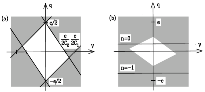
indicate the parameter region where one of the Eqs. (192)–(195) is fulfilled as an equality. The area inside these lines is the region where the island charge is stable because all tunneling rates vanish. In the shaded areas one or more rates are different from zero. Suppose now that we have an ideal double junction system without offset charges so that the effective island charge is given by . If and then the rates force the electrons to tunnel in such a way that after some time the island charge is zero. The state is stable in this voltage regime since all rates vanish. As a consequence at zero temperature there is no current if the absolute value of the voltage is below and we find a Coulomb gap even in the low impedance case. This important difference as compared to the case of a single junction is due to the charging energy related to the island charge.
If we now apply an offset charge either by placing a charge near the island or by using a transistor setup according to Fig. 16 with , the Coulomb gap will be affected. The possible effective island charges are then no longer given by but by . With this replacement we immediately get the tunneling rates for the single electron transistor from the double junction rates (184), (185), (187), and (188). The transistor rates then depend on , , and . Note that going from forward to backward tunneling rates now not only involves a change in sign of and but also of . To obtain the influence of the offset charge on the Coulomb gap we have to consider only charges in the range since an integer number of elementary charges can always be absorbed in . This means that for a transistor the stable island charge is not necessarily given by but depends on the gate voltage. However, if is in the range just mentioned the stable state will be . The situation for is shown in Fig. 21b. It becomes clear from this figure that the range in which is stable is decreased as compared to . For there is no voltage range for which an island charge is stable. This means that in the low impedance limit the Coulomb gap will vanish for . The dependence of the Coulomb gap on the offset charge is shown in Fig. 22.

For larger offset charges the picture is continued periodically with period according to the argument given above. Finally, we mention that the results for a low impedance environment may easily be generalized for a transistor with finite gate capacitance. If the transport voltage is divided symmetrically as shown in Fig. 16 one finds from (171) that the replacement and will account for the gate capacitance.[32]
6.5. Double junction in a high impedance environment
The similarity of the tunneling rates for single and double junctions shows also in the rate expressions for a double junction in a high impedance environment. For finite temperatures we obtain
| (196) |
which differs from the corresponding single junction result (85) only by the factor in front of which is due to the reduced coupling of the double junction to the environment. Accordingly, at zero temperature (196) reduces to . Together with (184) we then find for the forward tunneling rate through the first junction
| (197) |
By rewriting the energy difference as
| (198) |
it becomes clear that the local rule determines the zero temperature tunneling rates for a high impedance environment as it is the case for single junctions. Note that one may rewrite (198) in the local form (182) with a critical charge . This high impedance critical charge is unaffected by the reduced coupling to the environment since the local rule knows only about the capacitor of the junction through which the electron is tunneling. As for the low impedance environment we give the conditions under which the four rates are nonvanishing at zero temperature:
| (199) | |||||
| (200) | |||||
| (201) | |||||
| (202) |
These conditions are of course equivalent to the requirement that the charge on the junction should be larger than the critical charge . Again (199)–(202) define a region of stability for the state which is shown in Fig. 23.
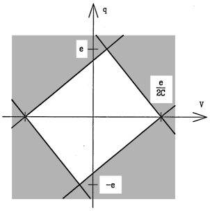
In comparison with the low impedance case this state is stable here for a wider range of parameters. In the absence of an offset charge the Coulomb gap is given by which always exceeds the low impedance Coulomb gap because . If offset charges are present we may apply the same arguments as for the low impedance case. We observe that in -direction the stable region extends over a range exceeding one elementary charge. As a consequence, one finds a Coulomb gap even for an offset charge where the gap vanishes for low impedance environments. The high impedance gap as a function of the offset charge is shown in Fig. 24.

Another consequence of this wide stability region in -direction is that for certain voltages two states with different island charges may be stable. Which one of the two states is realized depends on how the stability region is reached. Such a multistability may also result from a capacitor in series with the tunnel junction thereby producing a high impedance environment. This situation is discussed in more detail in Chap. 3 in connection with the single electron trap and related devices.
6.6. Current-voltage characteristics of a double junction
For a single junction the current could be calculated by subtracting the backward from the forward tunneling rate and multiplying this result by the elementary charge. This was possible since every tunneling process contributed to the current in the respective direction. For a double junction the situation is more complicated because the tunneling rates depend on previous tunneling processes which lead to a certain island charge. As we know from subsection 6.3. the tunneling rates depend on the external voltage and the effective island charge . The external voltage is taken to be constant and it is always assumed that electrostatic equilibrium at the double junction is established before the next electron tunnels. Then the state of the double junction is characterized by the number of electrons on the island. Neglecting correlations between different tunneling processes we may write down a master equation which connects states with different island charge. The probability to find the double junction in the state may change by leaving this state or by coming into this state from the states or
| (203) |
Here, is the rate for a transition from state to state . Since each tunneling process changes the island charge by the states and are neighbors on the island charge ladder with . There exist two independent possibilities to change the island charge, namely by tunneling through the first or through the second junction. Accordingly, the two rates have to be summed up yielding
| (204) | |||||
| (205) |
where we suppressed the dependence on the external voltage. In verifying these two relations one should keep in mind that the island charge is defined as , and hence an additional electron on the island decreases the island charge and thereby . Since we are not interested in the transient behavior we calculate the stationary probabilities by requiring . It is easy to see that probabilities satisfying the detailed balance condition
| (206) |
are a solution of the master equation (203). Since only nearest neighbor states are connected by nonvanishing rates it can be shown that this solution where the upward flow equals the downward flow is the only nontrivial solution. Starting from a neutral island one finds from (206) the stationary solution
| (207) |
and
| (208) |
with in both formulas. The only free parameter left is which is determined by the normalization condition
| (209) |
Knowing the stationary probability to find the island charge we may now calculate the current-voltage characteristics for a double junction from
| (210) |
Because of current conservation it does not matter for which junction we calculate the current. The equality of the second and third expression in (210) is ensured by the detailed balance condition (206).
While the above considerations are valid also for finite temperatures we will restrict ourselves to zero temperature to further illustrate the calculation of current-voltage characteristics. In the simplest case the voltage is below the gap voltage. According to our earlier discussions the state then is stable and only rates leading to a decrease of the absolute value of the island charge are nonvanishing. This means that the stationary solution of the master equation is given by , for . Since all rates vanish for we find from (210) that indeed the current vanishes in the blockade region. Let us now increase the voltage beyond the gap voltage for a double junction with different capacitances in a low impedance environment (cf. Fig. 21a). We begin by considering voltages satisfying . Setting , Fig. 21a tells us that tunneling of electrons through the first junction onto the island is allowed while tunneling through the second junction is forbidden. Being at the rates only allow the transition back to by tunneling through the second junction. Consequently, two states, namely and , are involved. From (208) and (209) one readily gets
| (211) |
and
| (212) |
The probabilities and together with (210) yield for the current
| (213) |
where the effective rate is given by
| (214) |
Since the two tunneling processes occur one after the other, the rates are added inversely and the total rate is dominated by the slower rate. We note that here is really only an effective rate because the two step tunneling process does not lead to a purely exponential time dependence. Still is the average time between tunneling events across the double junction system.
Let us now increase the voltage to the regime where . Assuming we are sure that it is not possible that the island is charged with two electrons. According to Fig. 21 we now have two possibilities to leave the state . Either an electron may tunnel through the first junction to the right or it may tunnel through the second junction to the right. Depending on what actually happens, the island charge is then either or . The island may not be charged further. Therefore, in the next step an electron has to tunnel through the other junction restoring the neutral island. We thus have two competing processes, namely and . These two mechanisms now allow for two subsequent tunneling processes occurring at the same junction. The sequence of tunneling through the two junctions is no longer fixed but contains a statistical element.
It is obvious that by increasing the voltage the situation will become more and more complicated. In the following section we will derive some properties of the current-voltage characteristic which also hold at higher voltages. In general, however, one has to resort to numerical techniques. It is rather straightforward to use (207)–(209) to determine the stationary probabilities and calculate the current-voltage characteristics by means of (210).
6.7. Coulomb staircase
In the first part of this subsection we will calculate the current through a double junction at zero temperature for special values of the voltage for the limits of low and high impedance environments. We will assume that the capacitances and of the tunnel junctions are equal while the tunneling resistances and may take arbitrary values. For the positive voltages in the low impedance case and in the high impedance case the tunneling rates are given by
| (215) | |||||
| (216) | |||||
| (217) | |||||
| (218) |
Here, and correspond to voltages and island charges , respectively. We calculate the occupation probabilities of the -th state by starting from . For one immediately finds from (216) that vanishes. Furthermore, we find from (217) that vanishes for and thus, according to (207), for . Together with (218) this means that vanishes for all for which . The detailed balance condition (206) thus yields
| (219) |
From similar considerations for one finds
| (220) |
Making use of the rates (215) and (217), the two equations (219) and (220) may be recast into
| (221) |
Exploiting properties of binomial coefficients, we find for the normalization condition
| (222) |
This determines and we finally get the probabilities
| (223) |
When this is combined with (210), we obtain for the current
| (224) |
Here, we have evaluated the current through the first junction and taken into account that the backward rate does not contribute. The first term in the sum is obtained from the normalization condition (209) while the second term is given by
| (225) |
The latter result may be derived by viewing as a function of and applying the same trick used to derive (53). From (224) and (225) we get our final result for special points of the current-voltage characteristic [10]
| (226) |
at voltages
| (227) |
or
| (228) |
Thus, for certain voltages the current-voltage characteristic touches an Ohmic current-voltage characteristic with resistance which is shifted by the gap voltage in the low impedance case and by in the high impedance case.
Let us now discuss the current-voltage characteristics between the voltage points for which we just calculated the current. To keep things as simple as possible we assume the tunneling resistance of the second junction to be very large compared to . Then the island will be charged through the first junction up to a maximum charge. Occasionally an electron will tunnel through the second junction resulting in a current through the double junction. From the condition (192) for a non-vanishing rate through the first junction, one finds that the maximum island charge is given by , where denotes the largest integer smaller or equal to the argument. In the limit the current in the presence of a low impedance environment then reads
| (229) |
At the voltages given by (227) we recover the current (226). Increasing the voltage we observe a jump in current by because the maximum island charge is increased by . This jump is followed by a linear current-voltage characteristic with differential resistance . This ensures the validity of (226) and (227). One may apply the same arguments for the high impedance case where the whole picture is just shifted in voltage by .
The steplike structure which we have found is called the Coulomb staircase.[34]–[37] It is very distinct if the ratio of the tunnel resistances is very different from one. For the steps are barely visible. For general parameters one has to evaluate (207)–(210) numerically. In Fig. 25

current-voltage characteristics are shown for low and high impedance environments as well as for the case of an Ohmic resistance . As for the single junction one finds for such a low conductance a crossover from the low impedance characteristic to the high impedance characteristic. For , the staircase need not be as regular as it appears for a double junction with equal capacitances.
In this section on double junction systems we mentioned in several places how the results have to be generalized to account for an offset charge . It is now straightforward to calculate current-voltage characteristics for different offset charges. As an example we present in Fig. 26

the zero temperature current-voltage characteristics of a single electron transistor in a low impedance environment. This figure shows the Coulomb staircase as well as the dependence of the Coulomb gap on the offset charge. The junctions chosen here have equal capacitances but a ratio of tunneling resistances to produce a marked Coulomb staircase. The offset charge changes from in the lowest curve to in the uppermost curve. As we have discussed already, the Coulomb gap depends on the offset charge. The middle curve with does not show a Coulomb gap as is expected from our earlier considerations. Furthermore, the characteristics for an offset charge different from 0 and exhibit an asymmetry. As we found earlier all orientations of tunneling processes are reversed if we make the replacement and . As and are equivalent offset charges we find that the characteristics for and should be identical to the characteristics for and and vice versa. This can clearly be seen in Fig. 26.
6.8. SET-transistor and SET-electrometer
In a SET-transistor setup like the one shown in Fig. 16 the current through the junctions depends on both the transport voltage and the gate voltage . So far we have mainly concentrated on current-voltage characteristics . In this section we will keep fixed and discuss how the current changes with the offset charge . The offset charge may be due to a gate voltage coupled capacitively to the island or due to some other mechanism. The dependence of the current on the offset charge can be exploited in two ways. By means of the gate voltage one may control the current thereby realizing a transistor.[4] On the other hand, one may use the current to measure the offset charge. In this case one uses the circuit as a very sensitive electrometer.[38] For the practical aspects of these devices we refer the reader to Chaps. 3 and 9. Here, we want to apply the results obtained above to the calculation of --characteristics. As in the previous sections it will not be possible to give a closed analytical expression for arbitrary transport voltages. We therefore restrict ourselves to the regime below the Coulomb gap voltage. Since the performance of the transistor and electrometer reaches an optimum when biased at the gap voltage, this is the regime of practical interest.
To be more specific, let us choose a setup with equal junction capacitances but arbitrary ratio of tunneling resistances . In practice, the assumption of a low impedance environment will be well satisfied. Furthermore, we restrict ourselves to the case of zero temperature. From the discussion of the current-voltage characteristics of a double junction it is clear how to generalize the calculation to finite temperatures. However, in this case one has to resort to numerical methods.
As already mentioned, we consider transport voltages below the low impedance gap . The offset charge is assumed to satisfy . Then, once a stationary situation is reached, only two island charge states are occupied (cf. Fig. 21b). Taking the transport voltage to be positive we find from (193) and (195) that the backward tunneling rates and vanish if the island charge takes one of the two allowed values. When initially and thus the tunneling rate through the first junction is nonvanishing while is zero according to (192) and (194). After an electron has tunneled through the first junction has changed to . Now, vanishes and is different from zero allowing the electron to tunnel from the island. We now have the same situation as described in Sec. 6.6. The corresponding Eqs. (211) and (212) read
| (230) |
and
| (231) |
Inserting these probabilities for the two possible island charge states we find with (210) for the current
| (232) |
According to (184) and (187), for equal capacitances the rates through the first and second junction are related by
| (233) |
Together with (191) and (181) we finally obtain for the current at fixed transport voltage
| (234) | |||||
The two step-functions are a consequence of the Coulomb gap. For very low transport voltages one needs an offset charge rather close to to obtain a current. As a function of the gate voltage the zero bias conductance thus displays a sequence of peaks at , integer. For semiconductor nanostructures these Coulomb blockade oscillations are discussed in great detail in Chap. 5. With increasing transport voltage the range of offset charges leading to a nonvanishing current becomes larger. Finally, if the transport voltage equals the gap voltage, the current only vanishes for as expected. Above this voltage the control of the current by the gate rapidly decreases and the performance of the transistor or electrometer is reduced as can be seen from Fig. 27.

For equal tunneling resistances the --characteristics at transport voltages below the gap voltage are given by parabolas symmetric to . This behavior is shown in Fig. 27a together with some curves at higher transport voltages. The environmental impedance is taken to be Ohmic and rather small (). If the tunneling resistance is much larger than the --characteristic (234) becomes
| (235) |
which at the gap voltage reduces to
| (236) |
In contrast to the parabolic characteristic obtained for the symmetric transistor we now have a sawtooth-like characteristic with the slope determined by the larger tunneling resistance. For the opposite case, , one finds from (234) at the gap voltage
| (237) |
i.e. a reversed sawtooth characteristic. Numerical results for a ratio of tunneling resistances and low Ohmic damping are presented in Fig. 27b. Note that by choosing an asymmetric transistor one may obtain a very high sensitivity for a certain range of offset charges. Fig. 27c shows numerical results for a rather large Ohmic impedance of the environment. Obviously the sensitivity on the offset charge is drastically reduced as compared with an electrometer embedded in a low impedance environment.
6.9. Other multijunction circuits
The methods we have discussed so far in this section are not only applicable to double junction systems but also to circuits containing more than two junctions. Such multijunction systems can exhibit interesting physical behavior and are therefore discussed extensively in other chapters of this book. We mention systems containing few tunnel junctions (Chaps. 3 and 9), one-dimensional arrays (Chap. 7), and two-dimensional arrays (Chap. 8).
The network analytical approach introduced in Sec. 6.2. may be applied to a general multijunction circuit. To calculate tunneling rates across a given junction the circuit can be reduced to an effective single junction circuit containing a tunneling element, an environmental impedance and an effective voltage source. Such a reduction becomes possible by applying the Norton-Thevenin transformation discussed earlier. To disentangle complex circuits one usually will also need the transformation between a star-shaped and a triangle-shaped network, the so-called T--transformation.[39] Generally, the effective impedance will contain a contribution diverging like for small frequencies. By splitting off this pole one separates the effective impedance into a capacitance related to the charging energy and an impedance describing the environmental influence. In this way, one directly finds expressions for the tunneling rates through the individual junctions as long as simultaneous tunneling through more than one junction is neglected. For a discussion of phenomena arising if co-tunneling is taken into account, we refer the reader to Chap. 6.
For the remainder of this section, we concentrate on the influence of the environment and choose as an example a one-dimensional array of tunnel junctions as shown in Fig. 28.

Although the network analysis for an array is straightforward, we shall first present here a more microscopic approach which brings out the underlying physics. For simplicity, we neglect a capacitive coupling to ground which may be present in a real setup and which is of importance for the description of charge solitons in one-dimensional arrays (cf. Chap. 7). For our purposes it is sufficient to consider the capacitances associated with the tunnel junctions carrying the charges . As for the single and double junction systems we introduce phases satisfying the commutation relations
| (238) |
To describe the environmental influence it is convenient to introduce another set of charges and phases. From the surrounding circuit the array of tunnel capacitors may be viewed as a single capacitor with total capacitance
| (239) |
carrying the total charge
| (240) |
In addition there are island charges
| (241) |
This set of charges is associated with a set of phases satisfying the commutation relations
| (242) |
with all other commutators vanishing. The two sets of phases are related by
| (243) | |||||
| (244) | |||||
| (245) |
as for the double junction system in Sec. 6.2. The operator describes tunneling through the -th junction. According to (244) this may be decomposed into an electron leaving the –1-th island and an electron entering the -th island . In (243) and (245) only one -operator occurs since tunneling through the first or last junction affects only one island charge. The operators are associated with the change of the total charge seen by the environment. Here, is the obvious generalization of (172) to the multijunction case. The relations (243)–(245) essentially contain all information we need to know about tunneling in a one-dimensional array. The change in electrostatic energy connected with a tunneling process consists of contributions arising from the change of island charges and a contribution from the work done by the voltage source to restore the total charge. The latter is given by since according to (243)–(245) the charge transferred to the voltage source after an electron has tunneled through the -th junction is . As in (180) for the double junction, the factor leads to a reduced influence of the environment due to a decoupling of the -th tunnel junction from the environment by the other junctions. The total impedance is thus effectively reduced by a factor . Assuming that the capacitances of the tunnel junctions are all of the same order, we find from (239) that the total capacitance is smaller by a factor . As a consequence, the influence of the environment on a -junction system is reduced by a factor as compared to a single junction. The assumption of a low impedance environment is therefore usually well satisfied.
To determine the tunneling rates we first derive an explicit expression for the internal charging energy due to the island charges. Solving (240) and (241) for the charges on the junctions we find
| (246) |
After some algebra one obtains for the internal charging energy of the array
| (247) |
with
| (248) |
Here, is the inverse of the capacitance matrix
| (249) |
We note that the structure of (247) is also valid for more complicated multijunction circuits (cf. Chap. 3). Only the explicit form of the capacitance matrix will differ.
As a generalization of the energy difference (181) for electron tunneling in a double junction system we have for the one-dimensional array the changes in electrostatic energy
containing contributions from the change in the internal charging energy as well as from the work done by the voltage source. While the general structure of becomes very apparent if expressed in the set of variables the explicit form is rather complicated. On the other hand, we may as well choose the set of charges . Making use of (240) and (241) we then find from (6.9.) together with (247) the very simple result
| (251) |
with the critical charge
| (252) |
This is a straightforward generalization of the double junction result (182) and (183).
Before turning to the tunneling rates we will shortly outline how the result (251) can be obtained by network analysis. Considering electron tunneling through the -th junction, we may combine the other junctions into one capacitor of capacitance
| (253) |
carrying the charge
| (254) |
We thus have reduced the one-dimensional array to an effective double junction system. We now view the capacitances and as the two capacitances in a double junction system. Accordingly, and are the charges sitting on the two junction capacitors. Using our results from Sec. 6.2. we find an effective single junction circuit like the one depicted in Fig. 20c. The capacitor with effective capacitance
| (255) |
carries the charge
| (256) |
which corresponds to the island charge of a double junction. As already discussed above the effective impedance is given by and the effective voltage is . The difference in electrostatic energy is now readily obtained as
| (257) |
We are now in a position to write down the tunneling rates for a one-dimensional array. Using the same kind of reasoning as for the single junction or double junction we obtain for the forward tunneling rate through the -th junction [10]
| (258) | |||||
The backward tunneling rate is related to the forward tunneling rate by
| (259) |
and the detailed balance symmetry
It was pointed out above that the influence of the environment on the tunneling of electrons in a -junction array is reduced by a factor of the order of . This means that for most applications the low impedance limit will be correct. The rate expression (258) then reduces to the global rule result
| (261) |
which at zero temperature yields
| (262) |
As for the simpler circuits, the zero temperature rate is only different from zero if , i.e., if the charge on the -th junction exceeds the critical charge given by (252). This local formulation of the blockade criterion involving only the charge , the capacitance of the -th junction, and the capacitance of the surrounding junctions is of great importance for the understanding of few-junction systems (cf. Chap. 3).
Let us finally discuss the size of the Coulomb gap. As for the double junction system the stable state at voltages below the gap voltage is characterized by vanishing island charges . According to (246) the charges on the junctions are then all given by . Tunneling at the -th junction can therefore occur if . No current will flow if the voltage across the array is smaller than . Since , the gap voltage is determined by the junction with the largest capacitance. For an array with equal capacitances, i.e. , the low impedance Coulomb gap is given by . However, this gap and the Coulomb offset observed at large voltages where the high impedance gap appears, differ by .
Acknowledgements. We have benefitted from the interaction with numerous colleagues of whom we can name only few here. One of us (G.-L. I.) has enjoyed a fruitful collaboration with H. Grabert and would like to acknowledge discussions with P. Wyrowski and the members of the Quantronics Group at Saclay. The other author (Yu. V. N.) is grateful to T. Claeson, D. Haviland, and L. S. Kuzmin for discussions on experimental aspects of single charge tunneling and to A. A. Odintsov and M. Jonson for critically reading the manuscript on the microscopic foundation. He enjoyed the hospitality of the Fachbereich Physik at Essen where this chapter was written. We thank G. Falci for granting us permission to reproduce Figs. 13 and 14.
A. Microscopic foundation
A.1. Introduction
One may note that in the previous sections the tunnel junction was treated as the primary object. The whole electrodynamics was reduced to the network theory and the only trace of solid state physics was the one-electron Fermi distribution function. Therefore, one may call it ‘phenomenological approach’. It is difficult to underestimate its importance for applications. Nevertheless, there are some reasons to go deeper and to discuss the microscopic foundation of the method applied. First, the microscopic derivation is always a good way to test and probably to confirm the phenomenology. Second, the range of the applicability becomes clearly visible. Third, the interesting links between different approaches and different phenomena can be comprehended and some new effects can be described.
In this appendix we move from the microscopic description of the metals on both sides of the tunnel junction towards the phenomenology step by step. We encounter interesting physics on every step and have a general look on it.
We are starting with the formulation of the problem in a general way: how does the electromagnetic interaction affect the tunneling rate? We develop a semiclassical approach to electron motion and derive the basic formula which allows us to evaluate the effect in terms of Maxwell electrodynamics and a Boltzmann master equation description for the electrons. Then we discuss the fundamental relation between the voltage applied to the junction and the effective scales at which the tunneling electron feels the electrodynamic environment.
After that we apply our approach to Altshuler’s diffusive anomalies in the density of states.[40] Within this framework these anomalies and the Coulomb blockade appear to be two sides of one coin. While proceeding we consider the most important case when the field induced by the electron moves faster than the electron itself. It allows us to forget about this electron. Moving along this way we remind the reader of some simple electrodynamics in a metal-thin insulator-metal system and consider fingerprints of this electrodynamics on the tunnel junction - curve. In the very end we show how one can move from the continuous electrodynamics to the network theory finishing the consequent microscopic derivation of the phenomenological approach.
A.2. General problem
As it is widely known, it is easier to answer general questions than specific ones so that we try to formulate the problem in a most general way. Let us answer the question: How does the electromagnetic interaction affect the electron tunneling rate?
First, of course, this interaction forms the crystal lattice of metals and of the insulator layer through which the electrons tunnel. It determines the energy spectrum of elementary excitations in these condensed media and thus provides every decoration of the scene for this solid state physics performance. Everything is made here by the electromagnetic fields acting on the length, energy, and time scales of the order of atomic values. The question how it makes these things is in fact the basic problem of condensed matter physics and we are not going to solve it just here. We come on the scene formed and we are interested in the part of the electromagnetic field which is:
-
1.
slow enough not to change the electron energy on an atomic scale
-
2.
weak enough not to turn electrons from its trajectories
-
3.
described by linear electrodynamic equations
-
4.
basically uniform on the atomic scale.
We call it the low-frequency part of the electromagnetic interaction and will deal only with this part. Also we assume the voltage applied to the junction to be much less than the typical atomic energy or the Fermi energy for electrons. So we will operate on scales which are much larger than the atomic ones. One may call this formulation a mesoscopic problem but we prefer not to do it. The evaluation of the effect under consideration has been done in Ref. [41] by using the standard formalism of field trajectory integrals. This approach is inconvenient due to the use of an imaginary time representation and the relative complexity. Here we use another way to derive it which is based mostly on physical reasoning. This way can be compared with the one used in Ref. [42].
First let us note that on this scale a semiclassical approach to the electron motion is valid or, in simple terms, we can consider electrons as classical particles that are scattered and jump through the tunnel barrier. Switching off the low-frequency part of the electromagnetic interaction we introduce a probability to jump through the barrier at the point on the barrier surface with initial electron wave vector and wave vector after tunneling. Only the electrons near the Fermi surface can tunnel so we need to know this probability only on this surface. The tunneling is completely elastic because the interaction is switched off. The total tunneling rate then is given by
| (263) |
Here we integrate over belonging to the junction area, the two-dimensional wave vectors and parametrize the Fermi surface, the -function ensures the tunneling to be elastic, denote the densities of states per energy interval at the Fermi surface for the two metal banks, respectively, and is the Fermi distribution function.
Let us consider now the problem from the quantum mechanical point of view. We introduce the electron propagation amplitude connecting the electron wave functions at different times by [42]
| (264) |
Within the semiclassical approach the different classical trajectories contribute to without interfering with each other. If we are interested in evaluating the tunneling rate at a given point with given and there is a unique trajectory determined by these parameters which contributes. The phase of the propagation amplitude is proportional to the classical action along this trajectory:
| (265) |
This is the way to take the interaction into account. Let us note that electromagnetic interaction can be treated as the exchange of photons and as a first step consider the electron motion in the photon field. In accordance with the correspondence principle one should add to the total action the interaction term and thus obtain the propagation amplitude in the presence of a field:
| (266) |
with
| (267) |
Here, is the electron charge, and are the vector and scalar potential of the electromagnetic field, respectively, and and are trajectory parameters. On a large time scale the electron is scattered many times by impurities and the metal surface and the trajectory is extremely complicated. This is a reason to characterize this trajectory by the probability for the electron to be in the point with wave vector at time . It is worth to emphasize that the probability is conditional: the electron must jump at the point with certain and at time . Therefore, it is more convenient to rewrite (267) in the form
| (268) |
where
| (269) |
and
| (270) |
Here, is the time needed to move from to along the trajectory. A careful analysis shows that there is also a probability flow
| (271) |
at an belonging to the oxide barrier volume, where is a vector normal to the junction surface. The necessity of this term results from the conservation of probability flow. The barrier thickness is of the order of a few atomic sizes and at first look the contribution of this term to the action is much smaller than that of the probability flow in the metal. However, the electromagnetic field in the oxide barrier may be much larger than in the surrounding metals and therefore one has to keep this term.
Performing the field quantization we replace classical potentials by appropriate Heisenberg time-dependent operators. The propagation amplitude also becomes an operator. The tunneling rate at given energies , in initial and final states is proportional to the square of the Fourier transform of the propagation amplitude
| (272) |
where denotes the average over the equilibrium density matrix of the electromagnetic field and
| (273) |
In this equation and are chosen to be very far from the jump point in the one bank and in the other one, respectively. They can be characterized by the two traversal times needed to move from to and needed to move from to . For the square of the propagation amplitude reaches a certain limiting value related to the rate.
If we are not interested in relativistic effects concerning the electromagnetic field propagation we are able to omit the vector potential in (267) and (268). Using (268) we then obtain
| (274) | |||||
According to the previous considerations we can consider as the sum of a large number of boson operators as it has been considered within the phenomenological approach in Sec. 2.3. It allows us to use the simple rules for operator multiplication when calculating the square. For example,
| (275) | |||||
with
| (276) |
After some algebra one gets
| (277) |
where we introduced
| (278) |
with
| (279) |
The latter can be expressed in terms of the Fourier transforms of and the field correlation function :
| (280) |
| (281) |
The coefficient of proportionality in (277) can be determined if we switch off the electromagnetic interaction. Thus we obtain for the total tunneling rate as a nice generalization of (263)
| (282) | |||||
Now we should discuss what we have done. The physical picture in fact is rather simple. In (263) we replace the -function, which reflects the fact that in the absence of the interaction the tunneling is elastic, by the probability to have a certain energy change when tunneling in the presence of the interaction. This change is provided by emission or absorption of photons. Due to the semiclassical nature of electron motion and due to the small energy transfer for every emission/absorption act all of these acts happen independently. Thus for every photon energy the probability to emit a certain number of photons obeys the Poissonian statistics and (278) and (279) are simply a generalized mathematical formulation of this fact. Within the phenomenological approach this was discussed in Sec. 4.1. Within the microscopic theory we were able to express these photon emission/absorption probabilities in terms of the electron motion along the classical trajectory and the field correlation function. Thus we managed to simplify the problem considerably. Now, we can calculate the tunneling rate if we know all about classical electron motion and the electrodynamics in the region around the junction. Let us now express our results in a form appropriate for practical use.
First we express the field correlation function in terms of the response function by means of the fluctuation-dissipation theorem
| (283) |
Here is the advanced response function
| (284) |
which determines the field response to an external charge placed at point . It is convenient to consider as this external charge. is determined by the electrodynamic equations in a medium with a given source. It is easier to solve these equations than to completely calculate the response function . The result (279) may be rewritten in terms of as
| (285) |
To calculate the probability which characterizes the electron motion one may use the standard Boltzmann master equation approach. For example, for the probability to be on one of the banks after tunneling the Boltzmann equation reads
| (286) | |||||
Here, is the electron velocity in the state with a wave vector , is the scattering rate from the state with to the state with due to the impurities and the metal surface, and the source term describes the electron arrival from the other bank at . Often we need to describe the electron motion only on a time scale which is much larger than the time between the scattering events. In this case one may use the diffusion equation for the electrons:
| (287) |
with appropriate boundary conditions.
For the derivation of (282) we assumed a non-relativistic field. Strictly speaking this means that we are not able, for example, to describe the inductance in electric circuits. This is why it is worth to emphasize that all the field relativistic effects can be treated in the same manner. The most convenient gauge choice is and the field is described by the vector potential only. Acting along the same lines we express the answer
| (288) |
in terms of the vector potential correlation function
| (289) |
Here is the probability flow introduced earlier. It is also possible to simplify this form by introducing the vector potential response on the external current yielding
| (290) |
Now we are in a position to apply these general results to some illustrative examples.
A.3. Time of tunneling
Before making these applications it is important to discuss the relevant time scale on which we are going to operate. As far as we consider tunneling rates this relevant time should be the time of tunneling. The problem is not transparent and sometimes it leads to misunderstanding. To feel that let us consider the noninteracting electrons on a scale much larger then the atomic one. The electrons rush along the metal and sometimes jump through the tunnel barrier. The thickness of this barrier is of the atomic order and a jump takes no time. On the other hand, the tunneling is elastic and the energy loss equals zero. According to quantum mechanics, the energy uncertainty and the time for tunneling obey the relation . It means that the time for elastic tunneling is infinitely long.
So we have a real choice: from zero to infinity. This is natural since quantum mechanics always gives rise to duality. The answer depends on the way how the time of tunneling is introduced or, in practical terms, it depends on the quantity measured.
If we are sure that our tunneling is elastic there are many ways to introduce the traversal time (see [43] for a review) and sometimes to measure it [44]. In this case the time is determined by the properties of the electron’s motion under the barrier and there is some interesting physics due to the virtual nature of this motion. In contrast, for inelastic tunneling the voltage applied to the tunnel barrier and/or the temperature impose strict restrictions on the frequency of the radiation emitted/absorbed: . This frequency determines the time scale as can be seen from the previous equations. If the most part of the tunneling events are inelastic it also determines the time of tunneling. If it is not so this argument is applicable only for inelastic events.
Thus the tunneling may be characterized by two time scales. The case when these scales are of the same order is described in Refs. [42, 45]. Note that in this case the tunnel barrier is suppressed by the applied voltage.
The frequency scale specifies also the length scale since we are able to estimate the distance which the electromagnetic field or electrons propagate for a given time. It allows us to find the effective geometry of the junction or, in other terms, to determine whether it can be considered as a point or as an interface of two semi-infinite metal banks. The length scale increases with decreasing frequency so that the lower the voltage and temperature the further away is the horizon which the junction sees. However, we should emphasize that the length scale can not be determined unambiguously. The electrons and the field propagate with different velocity. Moreover, different types of electromagnetic excitations differ in its velocities. This makes the length scale and effective geometry dependent on the inelastic process under consideration.
A.4. One-photon processes: anomalies and fingerprints
Now we try to find the scale for the strength of the effect considered. To characterize this strength it is convenient to introduce the effective frequency dependent impedance which the electron feels when tunneling:
The value of this impedance in the frequency region considered governs the deviations from Ohm’s law. If this value exceeds the quantum unit of resistance the probability for many-photon processes is significant, the deviations are large, and the tunneling rate is strongly suppressed in comparison to Ohm’s law. If not, the most part of the tunneling events are elastic and there are only small deviations from an Ohmic behavior which are due to one-photon processes. Very roughly the effective impedance can be estimated as the resistance of a metallic piece on an appropriate length scale. Usually, on the microscopic scale this resistance is small in comparison with and the deviations from Ohm’s law are small. For our illustrative applications we use this fact and we will consider mostly one-photon processes.
Let us express the probability in terms of the impedance. To do this we expand the exponent in (278) with respect to . The first order dependence of on will be
| (293) |
where is the probability to emit one photon in a unit energy interval
| (294) |
The simple formula
| (295) |
valid at zero temperature reflects the influence of one-photon processes on the - curve. By the way there is an answer how one can observe this small deviations on the background of the main effect. These deviations are clearly visible on the differential conductance-voltage curve or on the second derivative of the current in the region of small voltages because Ohm’s law is linear. It is convenient to divide the observable deviations into two classes:
-
1.
anomalies: the anomalous power law is displayed in some voltage region,
-
2.
fingerprints: the deviation is localized near a certain voltage.
A.5. Diffusive anomalies
So-called zero-voltage anomalies were observed in tunnel junction experiments from the early sixties. As it is comprehended now they were caused by different mechanisms. The early explanation ascribed the whole effect to the scattering by paramagnetic impurities.[46] It was confirmed that this can sometimes produce such anomalies [47], but there was also an effect in the absence of these impurities.
In 1975, Altshuler and Aronov proposed a more fundamental mechanism to be responsible for zero-voltage anomalies.[48] They calculated the interelectron Coulomb interaction effect on the carrier density of states near the Fermi level. Although the contribution to the density of states was found to be small it influences the observed anomalies because it depends nonanalytically on the distance from the Fermi level. A relation of the same kind as Eq. (263) was applied to calculate the tunnel current. The densities of states in this relation were allowed to have a small energy-dependent part. This results in a square-root contribution to the conductance of a junction and in the transition from the square-root to the logarithmic dependence as the thickness of the electrodes is reduced. These dependencies were perfectly confirmed by the experiments of Refs. [49] and [50].
In our opinion, these results are correct but there are two points of criticism concerning the link between the tunneling rate and the density of states. A discussion of these points will probably allow to better understand the physics involved.
First, the relation used assumes the tunneling rate to be proportional to the density of states in the banks of the junction. This assumption is undoubtedly correct within a one-particle theory where only elastic tunneling is possible, but it is not satisfied when the interelectron interaction is included. If the interaction affects the density of states, it is not consistent to neglect it when calculating the tunnel current.
Second, we are quite pessimistic about the principal possibility to measure the electron density of states in the presence of interaction excluding only few cases. The density of states in the presence of interaction is defined and calculated as being proportional to the probability to annihilate an electron with a given energy at a given point. Under realistic circumstances the number of electrons is conserved. We therefore can not annihilate an electron but only pull it out at a point and then measure the energy of this electron. In fact, this is the way how the experimental methods work, from X-ray to tunneling methods. But if there is an interaction by which the electron may loose or gain energy when being pulled out, there is a fundamental restriction on the resolution of these measurements.
This is why we prefer to discuss the effect of the electromagnetic interaction on the tunneling rate but not on the density of states. Now, we obtain anomalies involved in the framework of the method presented above and we will find them to be due to inelastic tunneling.
Let us first consider two semi-infinite metals separated by an insulating layer. We assume the frequency scale related to the voltage and temperature to be less then the inverse electron momentum relaxation time . This assumption allows us to use a diffusion equation for describing the electron motion. In order to evaluate the effective impedance we first calculate the Fourier transform of the conditional probability . Solving Eq. (287) we obtain
| (296) |
Here, different signs refer to the different banks and is the distance from the point of tunneling. Now we should evaluate . To do this, we solve the electrostatic equation with external charge :
| (297) |
Here, is the charge density formed by the metal electrons. As it is known metals are electroneutral and the sum on the right hand side of (297) equals zero in the metal. The only point where it is not zero is the mere point of the tunneling. The potential difference produces a current in the metal with density , being the metal conductivity. Due to electroneutrality the total current through the point of tunneling must be equal to the flow of external charge through this point with the inverted sign. It allows us to obtain :
| (298) |
After integration over space we find for the effective impedance
| (299) |
With the aid of (295) we obtain for the anomaly of the tunneling current
| (300) |
The result is the same as in [48] if taking into account the surface effect [51] but now we can ascribe it to inelastic tunneling. The length scale is of the order and the impedance can be estimated as the resistance of a metal piece of that size. The resistance increases with decreasing size provided the size is less than the electron mean free path . The maximum value of resistance would be of the order of for a reasonable metal ( is the electron wave vector at the Fermi surface) and it ensures that the deviation is never comparable with the main current.
Now we change the effective geometry and let the electrodes be films of thickness . The above consideration is valid if and we now investigate the opposite limiting case . In this case we can treat the probability and voltage as to be approximately constant across the film. It is convenient to use Fourier transformation here with the wave vectors along the film plane. For we obtain
| (301) |
The calculation of is a little bit more complex. The films separated by the insulating layer can be considered as a large capacitor with being the capacitance per unit area. The voltage difference between the electrodes produces the finite density of charge per unit area . Due to the symmetry of the system, has different signs but equal magnitude on the different electrodes. This allows us to write down the conservation law for the charge density in the following form:
| (302) |
As the next step we obtain
| (303) |
may be interpreted as the diffusivity of the electric field. As a rule and the field propagates faster then the electron. To obtain the impedance we integrate over and note that the dominant contribution to the integral comes from a wide region of : . We can ascribe the effect neither to field nor to electron propagation: there is something in between. It is convenient to express the answer introducing the film sheet resistance
| (304) |
It differs from the one derived from the density of states by a logarithmic factor. This is natural because the approach of Refs. [40, 48, 51] does not take into account the field propagation induced by the tunneling electron.
As far as we know we considered here all observable anomalies related to electron diffusion. Considering the variety of other anomalies and the effect of the external circuit we needed not to take into account electron motion at all. The reason for that is the following:
A.6. Field moves faster than the electrons
Indeed this is the usual case as we already have seen when we considered field propagation along resistive films: the field diffuses faster than the electrons. If the resistivity of the electrodes is lower we encounter different types of electromagnetic excitations which can be as fast as the light and they effectively overtake electrons. Due to this fact the length scale for the electromagnetic field is much larger than that one for electron propagation. Thus the electromagnetic field is constant on the length scale for electrons. It means we can use the simplest expression for :
| (305) |
Different signs correspond to different banks. Integrating over in Eq. (291) we obtain the simple but promising result:
| (306) |
Here, the superscripts (1) and (2) refer to different banks. Now, we are allowed to omit the subscript ‘eff’ because we have the honest electrodynamic impedance defined as voltage difference between banks at point 0 provided that this is the voltage response to the current produced by the electron jumping over the tunnel barrier. We have made one more step towards the phenomenology.
As an application of Eq. (306) we consider the influence of the undamped electromagnetic excitations which can propagate along the junction interface. We will assume that the junction is large enough so that the typical time scale defined by voltage/temperature is much smaller than the time needed for the electromagnetic excitation to cross the junction. The existence of these undamped excitations is provided by the insulating layer which separates the metallic banks and which can be considered as an infinite capacitor characterized by the capacitance per unit area. To calculate the impedance we write down the balance equation for the charge density of this capacitor
| (307) |
where is the volume density of the electrical current taken on the metal surface ( is normal to the junction interface). Performing the Fourier transform in time and in space coordinates along the interface and expressing all in terms of the voltage difference we can rewrite the previous equation as
| (308) |
Here, we introduced the non-local link between the normal current and the voltage on the junction: . From the previous equation we have for the impedance
| (309) |
We need only the real part of the impedance to evaluate its effect on the - curve. While the excitations are undamped the poles of the impedance at every lie on the real axis and only these poles contribute to the real part. Thus for the real part of the impedance we obtain
| (310) |
where is the spectrum of electromagnetic excitations. To evaluate the effect we need to know only the capacitance and this spectrum.
Let us first consider plasma excitations. For a bulk metal the plasmons can not have an energy less than the plasma frequency . Nevertheless there are low energy plasma excitations localized on the junction interface. We consider them in some detail. The electrical field in the metal produces the current of electron plasma
| (311) |
The electrostatic potential in the metal obeys Coulomb’s law . It means that
| (312) |
and the electrical field on the metal surface is . Combining these relations together with (308) we obtain for the spectrum
| (313) |
and for the deviation of the tunnel current
| (314) |
We write ‘sign’ here in order to emphasize the non-analytical behavior of this deviation. As a rule the dimensionless factor on the right hand side of (314) is less than unity. For a reasonable thickness of the tunnel barrier of a few atomic lengths this coefficient is of the order . This ratio is less than unity for most metals.
One may note that the velocity of the plasma excitations increases with decreasing frequency so that at lower frequencies we should take into account relativistic effects omitted in the previous consideration. Actually, an electrical current in the plasma produces a magnetic field and an alternating magnetic field induces an electric one. Due to this fact the field penetration depth is restricted by the value of . By taking this fact into account the spectrum of electromagnetic excitations is given by
| (315) |
which describes the crossover between high frequency plasma excitations and low frequency Swihart waves. In terms of voltage this crossover occurs at
| (316) |
which is about 100 mV for aluminium. At lower voltages, we obtain for the deviation
| (317) |
where the velocity of the Swihart waves is .
Usually, the electrodes are thin metallic films. For low voltages when for a typical we have , where is the film thickness, the previous results should be modified. The velocity of electromagnetic waves in this system can be compared with the speed of light, so that Eq. (310) should also be modified. We present the result for the case [25]
| (318) | |||
Here, is the speed of electromagnetic excitations without taking into account relativistic effects, is the real speed, is the speed of light in the insulating layer and the Lorentz factor describes the relativistic effects.
There is a variety of different regimes of field propagation in this large area junctions and we will not review this matter here. Some of the cases were described in Refs. [25] and [52]. Now we return to small-area junctions which are mostly discussed in this book and consider the influence of finite size on the whole picture described above.
A.7. Junction-localized oscillations
We now concentrate our attention on the 100-10000 angstroms size junction that are under experimental investigation now. The time of electromagnetic excitation propagation along the whole junction corresponds to a voltage in the region from ten to several hundred microvolts. The excitations are practically not damped in this frequency region.
There are basically two ways to connect the junction with the contact wires: first, to interrupt the thin wire by the tunnel barrier; second, to form this barrier by overlapping of the two films. The junction area corresponds to the wire cross-section in the first case and may be much larger than the latter in the second case.
Consider now the electromagnetic excitation propagation along the junction. The first and the second case correspond to two-dimensional and three-dimensional geometries of the previous subsection, respectively. In the simplest case of a rectangular junction the boundary conditions permit only discrete values of . The modes with are junction-localized oscillations that can be excited by electron tunneling. The frequencies of these oscillations are simply , where are permitted values of the wave vector. These frequencies evidently remain discrete regardless of the actual junction form.
We can make use of the formulae in the previous subsection for the effect of excitations on the junction - curve if we replace the integration over by the summation over discrete values :
| (319) |
where is the junction area. This yields the very simple expression for the effect at
| (320) |
Here, is the charging energy of the whole tunnel capacitor having the capacitance . Eq. (320) is valid only if the speed of excitations is much smaller than the speed of light. Otherwise it should be multiplied by the Lorentz factor of Eq. (A.6.). Thus, every oscillation makes a fingerprint on the - curve at the corresponding voltage.
It is worth to compare these results with the predictions of the phenomenological theory. According to that one at voltages larger than the inverse time of discharge through the leads attached to the junction we have a linear - curve with offset . From (320) one may see that it is valid only if the voltage does not exceed the lowest energy of the oscillation spectrum. At the voltages which are corresponding to the oscillation energies the junction conductance is jumping. The magnitude of the jump can be determined from the fact that the - curve is gaining the additional offset at this point. If this frequency is -fold degenerate, the additional offset is . At high voltages a large number of oscillations can be excited by the tunneling electron and the asymptotic law is determined by the appropriate expression for the infinite-area junction.
If we take into account the oscillation damping and/or the finite temperature, the jumps gain a finite width. The appropriate expressions one may find in Ref. [25]. Therefore the offset obviously increases with increasing voltage. It shows how the applicability of the phenomenology is restricted.
Now we finish by opening
A.8. A gateway into networks
In the previous subsection we have said nothing about the mode with . The existence of this mode is a straightforward consequence of charge conservation: if the junction is included into some electrical circuit there should be a possibility for charge to go out of the junction, and modes with do not provide this possibility. In this zero mode the voltage difference is constant along the whole junction. Therefore, the mode dynamics does not depend upon the nearest junction environment but is determined by the external circuit. The phenomenological equations derived in the previous sections are completely valid for this dynamics, so that there is a gateway from the microscopic world to the networks created by human beings.
References
- [1] See e.g. M. Tinkham, Introduction to Superconductivity (McGraw-Hill, New York, 1975).
- [2] K. K. Likharev, IBM J. Res. Dev. 32, 144 (1988).
- [3] D. V. Averin and K. K. Likharev, J. Low Temp. Phys. 62, 345 (1986).
- [4] D. V. Averin and K. K. Likharev, in: Mesoscopic Phenomena in Solids, ed. by B. L. Altshuler, P. A. Lee, and R. A. Webb (Elsevier, Amsterdam, 1991), Chap. 6.
- [5] G. Schön and A. D. Zaikin, Phys. Rep. 198, 237 (1990).
- [6] U. Geigenmüller and G. Schön, Europhys. Lett. 10, 765 (1989).
- [7] Yu. V. Nazarov, Pis’ma Zh. Eksp. Teor. Fiz. 49, 105 (1989) [JETP Lett. 49, 126 (1989)].
- [8] M. H. Devoret, D. Esteve, H. Grabert, G.-L. Ingold, H. Pothier, and C. Urbina, Phys. Rev. Lett. 64, 1824 (1990).
- [9] S. M. Girvin, L. I. Glazman, M. Jonson, D. R. Penn, and M. D. Stiles, Phys. Rev. Lett. 64, 3183 (1990).
- [10] H. Grabert, G.-L. Ingold, M. H. Devoret, D. Esteve, H. Pothier, and C. Urbina, Z. Phys. B 84, 143 (1991).
- [11] G. Schön, Phys. Rev. B 32, 4469 (1985).
- [12] H. Haken, Rev. Mod. Phys. 47, 67 (1975).
- [13] A. O. Caldeira and A. J. Leggett, Ann. Phys. (N.Y.) 149, 374 (1983).
- [14] A. A. Odintsov, Zh. Eksp. Teor. Fiz. 94, 312 (1988) [Sov. Phys. JETP 67, 1265 (1988)].
- [15] D. V. Averin and A. A. Odintsov, Phys. Lett. A 140, 251 (1989).
- [16] For a proof see e.g. W. H. Louisell, Quantum Statistical Properties of Radiation (Wiley, New York, 1973).
- [17] R. Kubo, Rep. Prog. Phys. 29, 255 (1966).
- [18] H. Grabert, P. Schramm, and G.-L. Ingold, Phys. Rep. 168, 115 (1988).
- [19] P. Minnhagen, Phys. Lett. A 56, 327 (1976).
- [20] G.-L. Ingold and H. Grabert, Europhys. Lett. 14, 371 (1991).
- [21] G. Falci, V. Bubanja, and G. Schön, Europhys. Lett. 16, 109 (1991); Z. Phys. B 85, 451 (1991).
- [22] M. H. Devoret, D. Esteve, H. Grabert, G.-L. Ingold, H. Pothier, and C. Urbina, Physica B 165&166, 977 (1990).
- [23] M. Abramowitz and I. A. Stegun, Handbook of Mathematical Functions (Dover, New York, 1972).
- [24] S. V. Panyukov and A. D. Zaikin, J. Low Temp. Phys. 73, 1 (1988).
- [25] D. V. Averin and Yu. V. Nazarov, Physica B 162, 309 (1990).
- [26] D. V. Averin, Yu. V. Nazarov, and A. A. Odintsov, Physica B 165&166, 945 (1990).
- [27] Yu. V. Nazarov, preprint (1991).
- [28] N. R. Werthamer, Phys. Rev. 147, 255 (1966).
- [29] A. Maassen van den Brink, A. A. Odintsov, P. A. Bobbert, and G. Schön, Z. Phys. B 85, 459 (1991).
- [30] I. O. Kulik and R. I. Shekhter, Zh. Eksp. Teor. Fiz. 68, 623 (1975) [Sov. Phys. JETP 41, 308 (1975)].
- [31] H. Grabert, G.-L. Ingold, M. H. Devoret, D. Esteve, H. Pothier, and C. Urbina, in: Proceedings of the Adriatico Research Conference on Quantum Fluctuations in Mesoscopic and Macroscopic Systems, ed. by H. A. Cerdeira, F. Guinea Lopez, and U. Weiss (World Scientific, Singapore, 1991).
- [32] G.-L. Ingold, P. Wyrowski, H. Grabert, Z. Phys. B 85, 443 (1991).
- [33] A. A. Odintsov, G. Falci, and G. Schön, Phys. Rev. B 44, 13089 (1991).
- [34] K. K. Likharev, IEEE Trans. Magn. 23, 1142 (1987).
- [35] K. Mullen, E. Ben-Jacob, R. C. Jaklevic, and Z. Schuss, Phys. Rev. B 37, 98 (1988).
- [36] B. Laikhtman, Phys. Rev. B 43, 2731 (1991).
- [37] J.-C. Wan, K. A. McGreer, L. I. Glazman, A. M. Goldman, and R. I. Shekhter, Phys. Rev. B 43, 9381 (1991).
- [38] T. A. Fulton and G. J. Dolan, Phys. Rev. Lett. 59, 109 (1987).
- [39] See e.g. J. L. Potter and S. Fich, Theory of Networks and Lines (Prentice-Hall, London, 1963).
- [40] B. L. Al’tshuler and A. G. Aronov, in: Electron-Electron Interaction in Disordered Systems, ed. by A. L. Efros and M. Pollak (Elsevier, Amsterdam, 1985).
- [41] Yu. V. Nazarov, Zh. Eksp. Teor. Fiz. 95, 975 (1989) [Sov. Phys. JETP 68, 561 (1990)].
- [42] Yu. V. Nazarov, Phys. Rev. B 43 6220 (1991).
- [43] E. H. Hauge and J. A. Støvneng, Rev. Mod. Phys. 61, 917 (1989).
- [44] E. Turlot, D. Esteve, C. Urbina, J. M. Martinis, M. H. Devoret, S. Linkwitz, and H. Grabert, Phys. Rev. Lett. 62, 1788 (1989).
- [45] Yu. V. Nazarov, Sol. St. Comm. 75, 669 (1990).
- [46] J. Appelbaum, Phys. Rev. Lett. 17, 91 (1966).
- [47] J. M. Rowell, in: Tunneling Phenomena in Solids, ed. by E. Burstein and S. Lundquist (Plenum, New York, 1969).
- [48] B. L. Al’tshuler and A. G. Aronov, Zh. Eksp. Teor. Fiz. 77, 2028 (1979) [Sov. Phys. JETP 50, 968 (1979)].
- [49] R. C. Dynes and J. P. Garno, Phys. Rev. Lett. 46, 137 (1981).
- [50] Y. Imry and Z. Ovadyahu, Phys. Rev. Lett. 49, 841 (1982).
- [51] B. L. Al’tshuler, A. G. Aronov, and A. Yu. Zyuzin, Zh. Eksp. Teor. Fiz. 86, 709 (1984) [Sov. Phys. JETP 59, 415 (1984)].
- [52] Yu. V. Nazarov, Fiz. Tverd. Tela 31, 188 (1989) [Sov. Phys. Solid State 31, 1581 (1989)].