Quantum control of donor electrons at the Si-SiO2 interface
Abstract
Prospects for the quantum control of electrons in the silicon quantum computer architecture are considered theoretically. In particular, we investigate the feasibility of shuttling donor-bound electrons between the impurity in the bulk and the Si-SiO2 interface by tuning an external electric field. We calculate the shuttling time to range from sub-picoseconds to nanoseconds depending on the distance ( nm) of the donor from the interface. Our results establish that quantum control in such nanostructure architectures could, in principle, be achieved.
pacs:
03.67.Lx, 85.30.-z, 73.20.Hb, 85.35.Gv, 71.55.CnSilicon based structures are among the most promising candidates for the development of a quantum computer Kane (1998); Vrijen and et al (2000); Skinner et al. (2003); Barrett and Milburn (2003); Martin et al. (2003); Friesen et al. (2004); Kane (2005) due to the existing high level of nanofabrication control as well as the well-established scalability advantages of Si microelectronics. Different architectures have been proposed in which nuclear spin Kane (1998); Skinner et al. (2003), electron spin Vrijen and et al (2000) or electron charge Barrett and Milburn (2003) are used as qubits. All of these proposals ultimately rely on the quantum control of single electrons bound to donors. The ability to move or ‘shuttle’ electrons between a donor and the Si surface using external electric field is an essential element of Si quantum computer architectures because the measurement of the electron spin states can only occur at surfaces whereas the qubit entanglement takes place at the donor sites. In particular, this shuttling time must be much shorter than the spin dephasing time ( ms in bulk Si). Application of electrostatic potentials at surface electrodes would drag the electron from and to the donor allowing the manipulation of the electron-donor coupling. Quantum control of donor states is also a crucial consideration in Si device ‘roadmap’ as miniaturization of transistors leads to only a few dopants per device.
In this Letter we theoretically consider the problem of quantum control of donor-bound electrons near a Si-SiO2 interface. We investigate the precise extent to which a donor bound electron in the bulk (a few tens of nanometers from the interface) can be manipulated between the donor-bound state and a surface-bound state (within a few nanometers of the interface) by suitably tuning an external electric field applied perpendicular to the interface. We address two issues of paramount importance in this context: (i) How fast can this electron shuttling between the donor and the interface be done in realistic Si structures? (ii) Is the shuttled electron at the surface still localized in all three dimensions (which will allow to take it back to the donor) or is it a delocalized two-dimensional electron (which will make it impossible to measure its spin)? Our quantitative answers to these questions indicate that quantum control consistent with Si quantum computer architectures could, in principle, be achieved.
We consider a single electron bound to a substitutional P donor in Si, a distance from an ideally flat Si/SiO2 (001) interface, under an applied uniform electric field perpendicular to the interface. Although conceptually simple, this one-electron problem has no formal solution. The approach adopted here is based on well established approximationsKohn (1957); Stern and Howard (1967); Martin and Wallis (1978); MacMillen and Landman (1984), proposed in the context of conventional Si-based devices, and validated by extensive studies available in the literature Ando et al. (1982). The formalism, briefly outlined below, allows us to keep the essential physical aspects of the problem within a clear and realistic description. The Hamiltonian is written in the single-valley effective-mass approximation MacMillen and Landman (1984):
| (1) |
where , is the ratio between the transverse () and longitudinal () effective masses, accounting for the Si conduction band valley’s anisotropy, and . This equation refers to one of the band minima along , which become lower in energy for this geometry Ando et al. (1982). Lengths and energies are given in rescaled atomic units: nm and meV respectively, cm/kV, the electric field is given in kV/cm, and , where and are the Si and SiO2 static dielectric constants. The second term in Eq. (1) is the electric field linear potential, the third term is the donor attractive potential, and the last two terms are the donor and electron image potentials respectively. In this case , meaning that the images keep the same sign as their originating charges.
The overall potential profile for the donor electron along the -axis is schematically shown on the inset in Fig. 1. Note that this is equivalent to an asymmetric double-well configuration: The well near the interface is denoted by and the one around the donor site by . Assuming the wells are not coupled, we obtain variationally each well’s ground state, defining a basis set for the low-lying energy eigenstates of the double-well. Truncating the Hilbert space into this particular two-dimensional subspace, based on the double-well analogy, is meaningful only for sufficiently large donor-interface separations. If , a single well description is more appropriate MacMillen and Landman (1984), and we therefore limit the range of distances examined here to . Moreover, each well’s ground state must have an excitation gap to the first excited state that is much larger than , which sets an upper bound for the temperature as well as for . For , the interface does not play a role and the single-valley approximation breaks down Friesen (2005). Uncoupled effective mass Hamiltonians for the donor electron in the - and -regions are written as , , , with
| (2) |
and . The donor-related terms [third and fourth terms in Eq. (1)] are approximated in by their value at the interface: , providing confinement along - in the -region. Further assuming that leads to the 2-D parabolic potential approximation suggested in Ref. Kane and et al, 2000: . The barrier at the oxide interface is assumed to be infinite, so for . The following properly normalized variational forms were adopted for Kohn (1957); MacMillen and Landman (1984):
| (3) | |||||
| (4) |
where and are variational parameters chosen to minimize for . In we have used which gives better agreement with the exact wave-function for the infinite triangular well Stern (1972) than or , as well as a lower variational energy than , and essentially the same as . For , we find that and coincide with the Kohn-Luttinger (KL) variational Bohr radii for the isolated impurity (), where nm and nm.
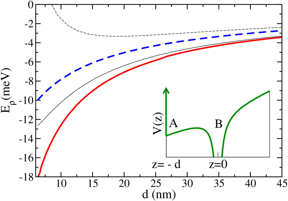
A relevant question in the present context regards the electron confinement parallel to the plane when it is drawn towards the interface (-region) by the field. It still remains bound to the donor through . The calculated energy as a function of , , is plotted in Fig. 1. The energy of the first excited state calculated variationally assuming the functional form , , is also shown. For nm, we get significant binding ( meV) for the ground state. Results obtained within the parabolic approximation are also shown in Fig. 1. As expected, this approximation underestimates the binding energies and overestimates the gap between successive levels, though convergence towards the variational results is obtained as increases. The variational parameter , characterizing the radial confinement of the ground state parallel to the interface, is given in Fig. 2(a). For the coherent manipulation of electrons in quantum devices, it is crucial that the entanglement of the electronic states occurs in a completely controlled and reversible manner. This requires that the ionized state near the barrier remains laterally bound to its respective donor site, setting an upper bound for the operating temperature [)] as well as for the donor planar density [] to avoid significant wavefunction overlap among electrons bound to neighboring donors. For nm, we get an excitation gap meV, and donor electron wavefunction confinement within a nm diameter region parallel to the interface. These parameters yield an upper bound of for planar donor densities and limit the operating temperature to a few K. Above these limits, the electrons at the Si surface would either form a delocalized impurity band () or become thermally excited ().
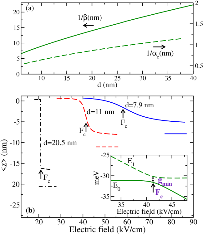
The double-well problem is solved through direct diagonalization of Eq. (1), , in the non-orthogonal basis , leading to the two lowest energy eigenstates and and eigenvalues and . The last term in the expression for is added to avoid double counting of the donor potential which is partially included in through . The response of the electron to an applied electric field is depicted in Fig. 2(b), where the expectation value is given for three values of . At very low fields the ground state is centered around the donor site , and its response to increasing fields is strongly dependent on : For the smaller values, the electron is smoothly drawn from near the P+ nucleus toward the barrier as increases, while for the larger the transition is more abrupt, and takes place at lower values of Smit et al. (2003); Martins et al. (2004). We define a critical field as the field value at which the gap is minimized, , characterizing the anticrossing point in a (, ) vs diagram [see inset in Fig. 2(b)]. For stronger fields , approaches . In this regime, the variational parameter characterizing the decay of the wavefunction along [see Eq.( 3)] becomes relevant. Fig. 2(a) gives the length vs for calculated at . We note that for the range of distances studied here, is always smaller than , justifying the double-well approach discussed above. For larger values of , confinement along the field direction becomes even stronger, with decreasing by about a factor of 3 as increases from to . The field-independent confinement length parallel to the interface, , is typically one order of magnitude larger than , and both increase sublinearly with increasing .
We now focus on a key parameter for general device applications: The tunneling time for donor ionization under an applied field. This question has traditionally been addressed in the literature Banavar et al. (1979) in analogy with the hydrogen atom ionization problem, based on the semiclassical WKB approximation. The expression for the tunneling time of an isotropic hydrogenic atom with effective Bohr radius in Si under a uniform electric field is Landau and Lifshitz (1977)
| (5) |
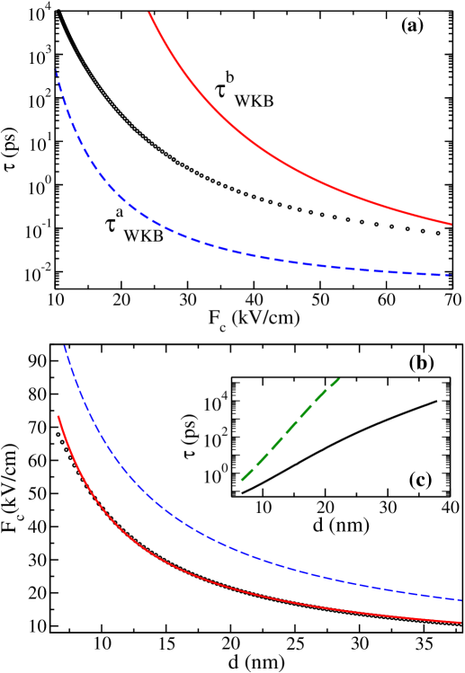
We present a fully quantum-mechanical estimate for the tunneling time, which we relate here to the anticrossing energy gap through the uncertainty relation. Fig. 3(a) presents our results for vs critical field, allowing direct comparison with the WKB estimates . Using for the KL variational Bohr radii and leads, respectively, to lower and upper bounds for the calculated , within a factor of up to 100 in the range of electric fields considered here. Our results cannot be fitted by the WKB isotropic model with an intermediate value of , a result that may be due to the intrinsically anisotropic nature of the system, to the final state in the ionized regime also being a bound state here, as well as to limitations of the semiclassical approximation.
A summary of our main results as a function of , which is the single fabrication-related parameter in our model system, is also presented in Fig. 3. Fig. 3(b) gives the critical field versus results, which are well fitted by the function , where is the saturation value of after complete donor ionization. Results varying as , obtained through a tight-binding model where the Si conduction band details, in particular its six-fold degeneracy, are incorporated Martins et al. (2004), are also given. The good qualitative agreement between the two curves indicates that our approach indeed captures the essential physical aspects of the system. The quantitative differences may arise not only from the single valley effective mass approximation adopted here, but also from the different geometries considered. These differences are manifest in the fact that the relevant distances in the phenomenological fittings are and respectively. Fig. 3(c) gives the tunneling times vs , showing that increases by 5 orders of magnitude as the donor distance to the interface increases by a factor of 5, with ranging from sub-picosecond to nanosecond time scales (e.g. ps for nm). Typical adiabatic passage times Martins et al. (2004) , also shown, are orders of magnitude larger than the tunneling time (e.g. ns for nm).
The results presented here define critical parameters to be taken into account in a variety of scenarios where these processes are involved. In silicon-based nano-electronic devices Ono et al. (2005), the critical field dependence on donor positioning and the tunneling time provide relevant information concerning threshold-voltage control and device switching times respectively. For the reversible manipulation of electrons in quantum devices, properties of the states bound to the interface define upper bounds for the operating temperatures and for the donor planar densities required () to avoid significant wavefunction overlap among electrons bound to neighboring donors. The times required for the shuttling processes will be different depending on whether quantum information is stored in spin or in charge degrees of freedom. In the case of spin qubits, tunneling times define the limiting time scales, since electron tunneling does not affect spin coherence. Spin coherence times in bulk Si (ms) Sousa and Das Sarma (2003) are at least 5 orders of magnitude longer than the tunneling times reported here. Moreover, spin coherence in Si can be further enhanced by isotopic purification Sousa and Das Sarma (2003); Tyryshkin et al. (2003). Recent experiments et al. (2005) demonstrate that is also sensitive to the dopant depth below the interface as well as to the interface quality. This means that, for the particular geometry of interest here, the Si bulk values of give an upper bound for the coherence times: Careful interface optimization as well as avoiding inhomogeneities in device fabrication and applied fields constitute additional requirements for a large number of operations to be performed before spin coherence is lost. For charge qubits, orbital/charge coherence is required and adiabatic evolution of the electron state must take place, requiring much longer time scales. Charge relaxation times are much shorter than spin coherence times, of the order of ns for Si quantum dots surrounded by oxide layers Gorman et al. (2005), but still longer than the adiabatic passage times for nm. Our realistic results provide physical bounds for quantum control of qubits based on Si:P donor electron states. In particular, provided that spin coherence times near a gated interface are reduced by no more than one order of magnitude as compared to the bulk values foo , gate-voltage induced spin manipulation on the single electron level may be feasible in donor-based Si quantum computer architectures, similar to the exciting recent experimental results on single electron manipulations in gated GaAs quantum dot nanostructures Petta et al. (2005).
We thank B. Kane and K. Brown for calling our attention to this problem. This work is supported by LPS and NSA. BK acknowledges support by CNPq and FAPERJ.
References
- Kane (1998) B. E. Kane, Nature 393, 133 (1998).
- Vrijen and et al (2000) R. Vrijen et al. , Phys. Rev. A 62, 012306 (2000).
- Skinner et al. (2003) A. J. Skinner, M. E. Davenport, and B. E. Kane, Phys. Rev. Lett. 90, 087901 (2003).
- Barrett and Milburn (2003) S. D. Barrett and G. J. Milburn, Phys. Rev. B 68, 155307 (2003); L. C. L. Hollenberg et al., Phys. Rev. B 69, 113301 (2004).
- Martin et al. (2003) I. Martin, D. Mozyrsky, and H. W. Jiang, Phys. Rev. Lett. 90, 018301 (2003).
- Friesen et al. (2004) M. Friesen et al., Phys. Rev. Lett. 92, 037901 (2004).
- Kane (2005) B. E. Kane, MRS Bulletin 30, 105 (2005).
- Kohn (1957) W. Kohn, Solid State Physics Series, vol. 5 (Academic Press, 1957), edited by F. Seitz and D. Turnbull.
- Stern and Howard (1967) F. Stern and W. Howard, Phys. Rev. 163, 816 (1967).
- Martin and Wallis (1978) B. Martin and R. Wallis, Phys. Rev. B 18, 5644 (1978).
- MacMillen and Landman (1984) D. MacMillen and U. Landman, Phys. Rev. B 29, 4524 (1984).
- Ando et al. (1982) T. Ando, A. Fowler, and F. Stern, Rev. Mod. Phys. (1982).
- Friesen (2005) M. Friesen, Phys. Rev. Lett. 94, 186403 (2005).
- Kane and et al (2000) B. E. Kane et al, Phys. Rev. B 61, 2961 (2000).
- Stern (1972) F. Stern, Phys. Rev. B 5, 4891 (1972).
- Smit et al. (2003) G. Smit et al., Phys. Rev. B 68, 193302 (2003).
- Martins et al. (2004) A. S. Martins, R. B. Capaz, and B. Koiller, Phys. Rev. B 69, 085320 (2004).
- Banavar et al. (1979) J. Banavar, D. Coon, and G. Derkits, Appl. Phys. Lett. 31, 94 (1979); T. Yamabe and A. Tachibana, Phys. Rev. A 16, 877 (1977).
- Landau and Lifshitz (1977) L. Landau and E. Lifshitz, Quantum Mechanics (Pergamon, 1977).
- Ono et al. (2005) Y. Ono et al., Jpn. J. Appl. Phys. 44, 2588 (2005).
- Sousa and Das Sarma (2003) R. de Sousa and S. Das Sarma, Phys. Rev. B 68, 115322 (2003); W. Witzel, R. de Sousa, and S. Das Sarma, Phys. Rev. B 72, 161306 (2005).
- Tyryshkin et al. (2003) A. M. Tyryshkin et al., Phys. Rev. B 68, 193207 (2003); E. Abe et al., Phys. Rev. B 70, 033204 (2004).
- et al. (2005) T. Schenkel et al., cond-mat/0507318 (2005).
- Gorman et al. (2005) J. Gorman, D. G. Hasko, and D. A. Williams, Phys. Rev. Lett. 95, 090502 (2005).
- (25) Even shorter values of T2 may be acceptable for experiments where spin-projection is the quantity of interest, and spin phase information is not relevant.
- Petta et al. (2005) J. R. Petta et al., Science 309, 2180 (2005); A. C. Johnsonet al., Nature 435, 925 (2005); F. H. L. Koppens et al., Science 309, 1346 (2005).