In situ resonant x-ray study of vertical correlation and capping effects during GaN/AlN quantum dots growth
Abstract
Grazing incidence anomalous x-ray scattering was used to monitor in situ the molecular beam epitaxy growth of GaN/AlN quantum dots (QDs). The strain state was studied by means of grazing incidence Multi-wavelength Anomalous Diffraction (MAD) in both the QDs and the AlN during the progressive coverage of QDs by AlN monolayers. Vertical correlation in the position of the GaN QDs was also studied by both grazing incidence MAD and anomalous Grazing Incidence Small Angle Scattering (GISAXS) as a function of the number of GaN planes and of the AlN spacer thickness. In a regime where the GaN QDs and the AlN capping are mutually strain influenced, a vertical correlation in the position of QDs is found with as a side-effect an average increase in the QDs width.
The control of growth processes is a major issue for the achievement of room temperature optoelectronic properties in nitride 3D nanostructures such as defect-free GaN/AlN quantum dots (QDs) Daudin et al. (1997). For that purpose the morphological characteristics and structural properties, namely the strain, size, size distribution, and density of QDs, must be controlled. X-ray techniques have shown their powerful abilities to monitor in situ these parameters over large assemblies of QDs Renaud et al. (2003). In this letter we report on a) an in situ strain analysis of the capping effect during the progressive covering of QDs by AlN, carried out with the Multi-wavelength Anomalous Diffraction (MAD) technique in grazing incidence, and b) an in situ study of the vertical correlation effect on the QDs size during the progressive stacking-up of GaN QDs planes Tersoff et al. (1996); Chamard et al. (2001); Gogneau et al. (2004), carried out by both Grazing Incidence Small Angle Scattering (GISAXS) and MAD.
Samples were grown on 6H-SiC(0001) substrates in a plasma assisted molecular beam epitaxy chamber installed on the French Collaborating Research Group beamline BM32 at the European Synchrotron Radiation Facility (Grenoble, France). The nitrogen flux was supplied by a radio-frequency plasma cell ; Knudsen cells provided the Ga and Al fluxes. The ultra-high vacuum environment made possible the in situ growth monitoring by Reflection High Energy Electron Diffraction (RHEED) and x-ray probes. Prior to GaN, a thin 8 monolayers (MLs) AlN buffer was deposited. The AlN surface quality was controlled by RHEED. Wurtzite GaN QDs were synthetized on top of AlN via the modified Stranski-Krastanow mode Gogneau et al. (2003), taking advantage of the in-plane 2.5% lattice mismatch between AlN and GaN. The QDs were grown at by depositing a GaN equivalent amount of 6 MLs. The first sample consisted of one GaN QDs plane progressively covered by 2, 4, 6, 8, 10, 12, 20, 27, 34 MLs of AlN. The second sample was a progressive stacking of 10 GaN QDs planes separated by 25 MLs AlN spacers. The third sample was made of 2 successive progressive stacks of 5 QDs planes separated by a) 25 MLs and b) 53 MLs AlN spacers.
A grazing incidence and exit setup was used to enhance the scattered x-ray signals from the QDs with respect to that of the substrate. Diffraction anomalous measurements were carried out around the Ga K-edge (10.367 keV). For the MAD experiments reciprocal space scans along the direction around h=3 were systematically recorded at 12 energies around the Ga K-edge using a point detector. The detector slits were opened so as to measure the integrated intensity over the grazing exit angle . A 2D charge-coupled device detector placed perpendicular to the incident beam was used for GISAXS measurements Renaud et al. (2003).
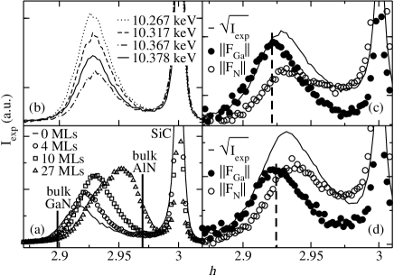
Figure 1(a) shows the evolution of h-scans close to the reflection as a function of the AlN coverage. These h-scans are related to both the in-plane strain state and size. The incident x-ray angle was fixed at , under the critical angle for total external reflection ( for bulk GaN in this energy range), so as to limit the scattering length below 10 nm and have surface sensitive measurements. With no AlN coverage, one observes a diffuse-scattering peak ascribed to QDs slightly strained by the AlN buffer and SiC substrate. As the AlN coverage increases, this peak is progressively distorted and shifted towards bulk AlN.
Further analysis was made possible by distinguishing the GaN contribution from the AlN and SiC contributions, using MAD measurements Ltoublon et al. (2004); Hodeau et al. (2001); Hendrickson (1991). Figure 1(b) shows some of the diffracted intensities measured in situ for a 8 MLs AlN coverage, at 12 energies across the Ga K-edge, taking advantage of the Ga anomalous effect to localize the Ga contribution along . For these measurements, the Ga partial structure factor of phase , that includes the Thomson scattering of all anomalous atoms (Ga), can be retrieved. In principle, the retrieval should be run in the framework of the Distorted Wave Born Approximation Pietsch et al. (2004); Schmidbauer et al. (2005). However, one can discard the energy dependence at the Ga K-edge of the reflection coefficients, as a consequence of the small Ga amount (6 equivalent MLs). Therefore, the recorded intensity corrected for fluorescence, , is proportional to the total square structure factor .
| (1) |
where . The partial structure factor of phase that includes the overall contribution of non anomalous atoms and the Thomson scattering of all anomalous atoms, , as well as , can be extracted for all h values, without any structural model by fitting eq. 1 to the experimental data with the NanoMAD algorithm Favre-Nicolin .
As shown in fig. 1(c,d), was extracted and , the complex structure factor of non anomalous atoms, was deduced from the extracted and , taking into account the wurtzite crystallographic structure. For h smaller than 2.985, i.e. far from the SiC substrate peak, only Al and N contribute to . The h position of the diffuse and peak maximum is inversely proportional to the in-plane lattice parameter, since where and .
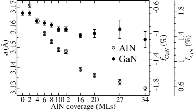
Figure 2 depicts the evolution of the in-plane lattice parameters and mismatches in both AlN and GaN, as a function of the AlN cap layer thickness. The lattice mismatch in the material, relative to the corresponding bulk material, is . It is clearly demonstrated that the AlN capping initially stressed by the QDs () is then progressively relaxed. Two different regimes can be distinguished, in which QDs and AlN capping are mutually influenced. A rapid decrease is observed until 16 MLs, followed by a more gentle diminution probably lasting after 34 MLs. Even for large AlN deposits (100 nm, not shown in Fig. 2) AlN remains slightly expanded (). Jointly the partially relaxed () surface QDs are gradually compressed by the AlN capping untill 16 MLs, leading to a plateau at , keeping in mind the large uncertainties for AlN coverage thicker than 16 MLs. Interestingly, the AlN strain state varies only very slowly above an AlN thickness of 30 MLs (7.5 nm). Under this semi-quantitative limit, the AlN tickness is such that the presence of buried dots significantly affects the AlN strain state, and a GaN QDs vertical correlation is expected.
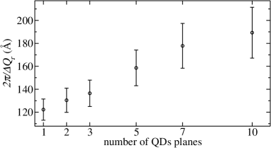
Another grazing incidence MAD study has been carried out for a gradual QDs planes stacking. The AlN spacer was chosen in a regime of mutual QDs and AlN influence and fixed at 25 MLs. and were extracted for 1, 2, 3, 5, 7, and 10 capped QDs planes, in order to obtain an information regarding the finite-size of GaN domains. Indeed, the full width at half maximum of in radial scans is related to the size by the Scherrer-like formula
| (2) |
where the broadening along the scattering vector , being the width of the peak along the h direction. Equation (2) assumes that the broadening by a strain distribution effect is negligible Renaud et al. (1999). The evolution of with the number of plane in the stack is plotted in Figure 3. Despite the 10% uncertainties, an increase of 50% in the size of QDs is put in evidence, as a consequence of a vertical correlation effect.
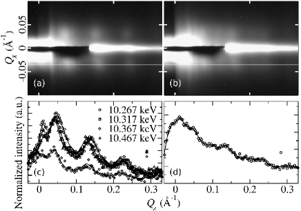
The vertical correlation effects were further investigated by anomalous GISAXS. The incident angle was set slightly above the critical angle, making the technique sensitive to the whole stacking. Figure 4(a) shows GISAXS measurements for a stack of 5 QDs planes separeted by 25 AlN MLs. The occurrence of satellites at is an evidence for the QDs position vertical correlation, i.e. along the direction Stangl et al. (2004); Chamard et al. (2003). Note that the period of these satellites, , corresponds to a stack period , i.e. the bilayer thickness. The strong energy dependence at the Ga K-edge of these satellites (Fig. 4(c)) confirms that the scattering yield is mainly from the QDs. Finally, fig. 4(b) shows a GISAXS map measured for a QDs planes stacking with 53 MLs AlN spacers. Compared to the case of thiner (25 MLs) AlN spacers (Fig. 4(a,c)) 53 MLs AlN spacers (Fig. 4(b,d)) seem large enough to inhibit the vertical correlation effects, likely because they are out of the regime of QDs and AlN mutual influence. This is consistant with the above conclusion that the critical thickness of the AlN spacer requested to allow correlation lays around 30 MLs.
In summary, the in situ diffraction analysis of the capping has shown that the strain state for the AlN spacer is influenced by the buried QDs up to 30 MLs of AlN capping, which corresponds to the upper limit (7.5 nm spacers) to observe correlation between successive GaN layers. More specifically, the connection between capping effects and vertical correlation effects was put in evidence. In particular it was shown that in a regime where the GaN QDs and the AlN capping are mutually strain influenced, a vertical correlation in the position of QDs is enabled with, as a side-effect, an average increase in the QDs width.
The authors would like to thank Y. Genuist, Y. Cur, M. Lafossas, and M. Noblet-Ducruet for their precious technical assistance.
References
- Daudin et al. (1997) B. Daudin, F. Widmann, G. Feuillet, Y. Samson, M. Arlery, and J. L. Rouvire, Physical Review B 56, 7069 (1997).
- Renaud et al. (2003) G. Renaud, R. Lazzari, C. Revenant, A. Barbier, M. Noblet, O. Ulrich, F. Leroy, J. Jupille, Y. Borensztein, C. R. Henry, et al., Science 300, 1416 (2003).
- Tersoff et al. (1996) J. Tersoff, C. Teichert, and M. G. Lagally, Physical Review Letters 76, 1675 (1996).
- Chamard et al. (2001) V. Chamard, T. H. Metzger, E. Bellet-Amalric, B. Daudin, C. Adelmann, H. Mariette, and G. Mula, Applied Physics Letters 79, 1971 (2001).
- Gogneau et al. (2004) N. Gogneau, F. Fossard, E. Monroy, S. Monnoye, H. Mank, and B. Daudin, Applied Physics Letters 84, 4224 (2004).
- Gogneau et al. (2003) N. Gogneau, D. Jalabert, E. Monroy, T. Shibata, M. Tanaka, and B. Daudin, Journal of Applied Physics 94, 2254 (2003).
- Ltoublon et al. (2004) A. Ltoublon, V. Favre-Nicolin, H. Renevier, M. G. Proietti, C. Monat, M. Gendry, O. Martry, and C. Priester, Physical Review Letters 92, 186101 (2004).
- Hodeau et al. (2001) J.-L. Hodeau, V. Favre-Nicolin, S. Bos, H. Renevier, E. Lorenzo, and J.-F. Brar, Chemical Reviews 101, 1843 (2001).
- Hendrickson (1991) W. A. Hendrickson, Science 254, 51 (1991).
- Pietsch et al. (2004) U. Pietsch, V. Holy, and T. Baumbach, High-resolution x-ray scattering : from thin films to lateral nanostructures (Springer Verlag, 2004).
- Schmidbauer et al. (2005) M. Schmidbauer, D. Grigoriev, M. Hanke, P. Schffer, T. Wiebach, and R. Khler, Physical Review B 71, 115324 (2005).
- (12) V. Favre-Nicolin, unpublished.
- Renaud et al. (1999) G. Renaud, A. Barbier, and O. Robach, Physical Review B 60, 5872 (1999).
- Stangl et al. (2004) J. Stangl, V. Holy, and G. Bauer, Reviews of Modern Physics 76, 725 (2004).
- Chamard et al. (2003) V. Chamard, T. H. Metzger, M. Sztucki, V. Holy, M. Tolan, E. Bellet-Amalric, C. Adelmann, B. Daudin, and H. Mariette, Europhysics Letters 63, 268 (2003).