Comparative study of the catalytic growth of patterned carbon nanotube films
Abstract
Three different catalysts (Fe, Ni, Co nitrates dissolved in ethanol) were patterned on a SiO2/Si substrate and multi-wall carbon nanotubes were grown by catalytic decomposition of acetylene. We compare the growth of the carbon nanostructures in the temperature range between 580∘C and 1000∘C. With our experimental set-up the catalyst solutions of cobalt and nickel were found to be less efficient than the one of iron. An optimal production of multi-wall nanotubes was observed at temperatures between 650∘C and 720∘C with the iron solution as catalyst. We found a tendency towards thicker structures with higher temperatures. Finally, we suggest a mechanism for the growth of these carbon structures.
I Introduction
Carbon nanostructures like fullerenes SMALLEY , nanotubes IIJIMA , nano-onions UGARTE and nano-horns TAKAHASHI have attracted much interest recently. In particular their mechanical and electronic properties are the subject of intensive studies FORRO ; LIEBER . Beside the fundamental interest in their physical and chemical properties, there are already some applications based on carbon nanotubes. For example, they are capable to work as efficient field emitters CHATELAIN and can form a basis for very robust fibers POULIN . Nanotubes can be produced by arc discharge IIJIMA , by laser-ablation SMALLEY2 or by chemical vapor deposition techniques (CVD) ZHANG ; LUCAS ; KERN ; PROVENCIO ; KIM ; KIM2 ; HAN . CVD is currently the most promising and flexible method with regard to applications, but our understanding of the influence of the catalyst and the deposition parameters on the nanotube growth is still fragmentary.
We use here the CVD method in combination with microcontact printing to grow patterned films of multi-wall carbon nanotubes KERN . Microcontact printing (CP) has become an often applied method in the last few years because it is a simple way to define chemical patterns on a variety of substrates DELAMARCHE ; WHITESIDES ; WHITESIDES2 . We use this method to selectively deliver a catalyst to the substrate surface, which in turn activates the growth of nanotubes KERN . The advantage of the patterning is that one can compare the regions with and without catalyst, and thus exactly determine the role of the catalyst. In order to better understand the catalytic growth we systematically examined the parameters temperature, catalyst composition and concentration.
II Experimental methods
II.1 Synthesis of nano-structured material
100-oriented boron doped silicon with the native SiO2 oxide layer was used as substrate. The stamps for CP were prepared by curing poly(dimethyl)siloxane (PDMS) for at least 12 h at 60∘C on a structured master prepared by contact photolithography. The width of the square patterns on the wafer is 5 m. The stamps were subsequently hydrophilized by an oxygen plasma treatment (O2 pressure 0.8 mbar, load coil power 75 W, 60 s). The stamp was loaded with 0.2 ml of catalyst solution for 30 s and then dried in a nitrogen stream for 10 s.
The solutions were Fe(NO3)9H2O, Ni(NO3)6H2O or Co(NO3)6H2O dissolved in ethanol at concentrations between 50 and 200 mM. The solutions were used 12 h after preparation because the metallic ions in the solution form chemical complexes which become larger with time. A period of 12 h for this “aging” of the solution was found to be ideal for the catalytic growth of nanotubes KERN . The printing was performed by placing the stamp on the surface of the SiO2/Si wafer for 3 s.
The samples were placed in a horizontal flow reactor (quartz tube of 14 mm diameter in a horizontal oven) directly after the printing. The treatment in the CVD oven proceeded in three steps. In the first step, the catalyst was annealed for 20 min under a flow of 80 ml/min of nitrogen to roughen the surface of the catalyst and to clean the reactor atmosphere. The actual deposition was performed with 80 ml/min of nitrogen plus 20 ml/min of acetylene (carbon source for the catalytic growth) at atmospheric pressure for 30 min. The third step was a final annealing of 10 min. under 80 ml/min of nitrogen. The same temperature was used throughout the entire procedure, which implies that a change of the temperature affected all the steps.
II.2 Characterization techniques
Scanning electron microscopy (SEM) was performed to analyze the microstructures in plan view. A Philips XL 30 microscope equipped with a field emission gun (FEG) operating at an acceleration voltage between 2 and 5 kV, a working distance of typically 10 mm, and in secondary electron (SE) image mode was used.
The growth morphology of the tubular structures and their crystallinity were controlled by transmission electron microscopy (TEM). For this purpose a Philips EM 430 microscope equipped with a Gatan image plate operating at 300 kV (point resolution 0.3 nm) was used.
III Results
We studied systematically the influence of (a) the catalyst solutions containing iron, nickel or cobalt ions, (b) the deposition temperature and (c) the concentration of the catalyst on the nanotube growth. We used concentrations of 50 mM and 100 mM of the three catalysts at temperatures between 580∘C and 1000∘C in 70∘C steps. For the catalyst iron, which produced the highest amount of nanotubes, we also examined samples with a concentration of 150 mM and 200 mM at 650∘C.
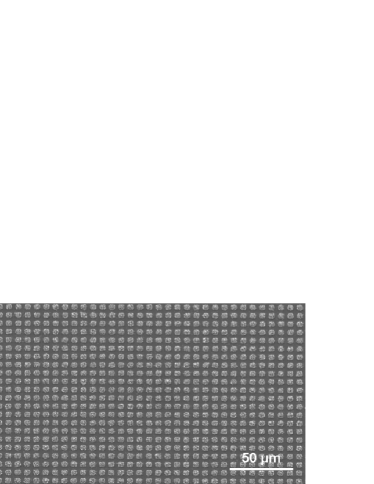
After the catalytic growth of the structures, the observation by SEM showed a homogeneous growth over the whole sample surface (1 cm2, Fig. 1). The nanotubes grow only where the catalyst has been printed, and the bare substrate is free of any carbon form for growth temperatures below 800∘C.
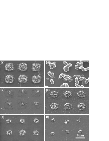
As displayed in Fig. 2, we found that the use of the iron catalyst resulted in the highest fidelity of replication of the square pattern, whereas the use of a pure nickel or cobalt solution resulted in inferior patterning. Because of the wetting behavior on the stamp KERN , the nickel and the cobalt solutions produced one drop on each square structure of the stamp, which were transferred to the substrate. As a result, the patterns obtained with cobalt and nickel are small and of irregular, circle-like shape. At concentrations higher than 100 mM the printing of the iron solution became also more difficult. XPS and TEM experiments have shown that the printed iron catalyst consists of a gel-like material of partially hydrolyzed Fe(III) nitrate that forms a porous and continuous Fe2O3 film after annealing SCHLAPBACH . We assume that the printed catalysts nickel and cobalt are of a similar structure.
The comparison of the three catalysts shows that iron produced the highest density of carbon structures at any considered temperature, as seen in Fig. 2. Nickel and cobalt turned out to be not as good catalysts as iron, as we found only few nanotubes at 720∘C with 100 mM nickel and cobalt solutions. At 1000∘C, the printed nickel and the cobalt solution initiated the growth of spherical carbon structures, and iron caused the growth of thick worm-like structures.
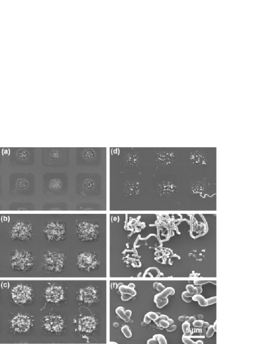
There is a tendency towards thicker structures with increasing temperature RODRIGUEZ , as shown in Fig. 3 for iron. The catalytic growth of nanotubes started at a temperature of 620∘C, but we observed only a few nanotubes at this temperature. A uniform coverage of each printed square was obtained at temperatures of 650∘C and higher. The thinnest nanotubes were found at 650∘C with iron as catalyst. The highest density of nanotubes was observed at 720∘C. Using catalyst concentrations of 100 mM we found relatively thick worm-like structures at temperatures exceeding 930∘C (“carbon worms”). These structures grew to a diameter of up to 1 m. Furthermore, the acetylene starts to dissociate in the gas phase at temperatures above 800∘C and the resultant carbon forms a amorphous continuous layer on the silicon surface of all samples. This layer gets also thicker with the temperature.
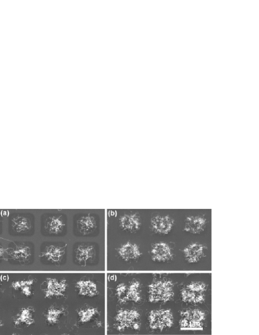
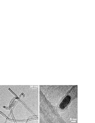
Fig. 4 shows clearly that the use of higher catalyst concentrations resulted in an increase of the nanotube density. The nanotubes reached lengths of several m with a diameter up to 25 nm. Transmission electron microscopy (TEM) of the samples obtained at 650∘C using the 50 mM iron catalyst confirmed that the structures are well-graphitized and well-separated multiwalled nanotubes which are not filled (Fig. 5). Most of them have open ends and some nanotubes contain encapsulated catalyst particles. These particles are aligned in the growth direction and of prolate shape. They have diameters of about 8 nm and lengths of about 16 nm.
IV Discussion
We suppose that the mechanism of the catalytic growth of carbon nanotubes is similar to the one described by Kanzow et al. DING . The acetylene is dissociated catalytically at facets of well defined crystal orientation of a small metal (oxide) particle. The resulting hydrogen H2 is removed by the gas flow whereas the carbon diffuses into the particle. For unsaturated hydrocarbons this process is highly exothermic. When the particle is saturated with carbon, the carbon segregates on another, less reactive surface of the particle, which is an endothermic process. The resulting temperature gradient supports the diffusion of carbon through the particle. To avoid dangling bonds, the carbon atoms assemble in a sp2 structure at the cooler side of the particle, which leads to the formation of a nanotube.
The growth of nanotubes starts at temperatures of 620∘C because there is enough mobility of the atoms of the catalyst to enable the diffusion of the carbon through the particle and to start the dynamic of the catalytic construction of carbon nanotubes. At temperatures above 800∘C the acetylene starts to dissociate already in the gas phase. The carbon in the gas flow of acetylene and nitrogen forms carbon flakes which will be adsorbed on the surface of the sample as well as on the surface of the structures (see Ref. ELSER ). Since the acetylene is not completely dissociated and the catalytic growth proceeds, the nanotubes will still grow and be covered with a layer of carbon formed by the carbon flakes. The structures get thicker with temperature because the proportion between dissociated and molecular acetylene increases.
We found only few nanotubes using nickel and cobalt as catalysts, whereas other groups successfully used nickel PROVENCIO ; KIM2 , nickel-cobalt KIM or cobalt LUCAS . This may be due to several facts. First, the catalyst is usually deposited by thermal evaporation or sputtering from a pure metal source. Furthermore, the catalyst is often reduced before the growth or the growth itself is carried out in a reducing atmosphere to ensure that the catalyst remains metallic RAO . In our case however, the catalyst is dissolved in a solution. Since the printed iron catalyst consists of a gel-like material that forms a Fe2O3 film after annealing KERN and no step is taken to reduce the catalyst, we conclude that in our case the catalyst is not pure metal, but metal oxide. This may significantly change the behavior of the catalyst. Second, we use thermal CVD, in contrast to the Hot Filament or Plasma Enhanced CVD used in other studies. The hot filament and the plasma provides an additional possibility for the dissociation of the hydrocarbon and may decisively influence the reaction kinetics.
The electronic properties and the enormous length-diameter ratio of the carbon nanotubes offers the possibility to use them as field emitters CHATELAIN . The non-aligned arrangement of the carbon nanotubes is known to be even more efficient in field emission than an aligned one KERN3 . The emission from aligned nanotube films is lower because of screening effects between densely packed neighboring tubes and the small height of the few protruding tubes. In contrast, the non-aligned films offer well separated nanotubes which do not show these effects CHATELAIN2 . For the sake of profitability their application in field emission displays requires glass as substrate instead of silicon, but the borosilicate glass used melts around 660∘C. Most studies carried out on catalytic nanotube growth use however temperatures above 700∘C LUCAS ; KIM , which are too high for that purpose. Choi et al. report a plasma-enhanced CVD process at a temperature of 550∘C KIM2 , but the diameter of these nanotubes seems quite large and lacks uniformity. We could demonstrate that the growth of thin carbon nanotubes with just a few layers of carbon starts around 620∘C, and that high quality films are obtained at 650∘C. These nanotubes have uniform diameter and well-graphitized walls which is an indicator for good field emission properties. The temperature may even be further lowered by using other gas mixtures, by using other metallic or heterogeneous catalysts HAN .
V Conclusions
We observed a significant influence of the temperature and the catalyst material on the quality of the carbon nanostructures. The diameter of the nanotubes and the density is adjustable by choosing the corresponding temperature and/or the concentration of the catalyst solution. Under the studied conditions iron is the best catalyst. We observed a morphology transition with temperature from multi-wall nanotubes to “carbon worms”. The best nanotubes are obtained at temperatures between 650∘C and 720∘C. Nanotubes obtained at temperatures below the melting temperature of borosilicate glass of 660∘C are suitable as field emitters for flat panel displays.
Acknowledgement
The Swiss National Science Foundation (SNF) is acknowledged for the financial support. The electron microscopy was performed at the Centre Interdépartmental de Microscopie Electronique (CIME) of EPFL.
References
- (1) H. W. Kroto, J. R. Heath, S. C. O’Brian, R. F. Curl and R. E. Smalley, Nature 381 (1985) 162.
- (2) S. Iijima, Nature 354 (1991) 56.
- (3) D. Ugarte, Nature 359 (1992) 707.
- (4) S. Iijima, M. Yudasaka, R. Yamada, S. Bandow, K. Suenaga, F. Kokai and K. Takahashi, Chem. Phys. Lett. 309 (1999) 165.
- (5) J. P. Salvetat, A. J. Kulik, J. M. Bonard, G. Andrew, D. Briggs, T. Stöckli, K. Méténier, S. Bonnamy, F. Béguin, N. A. Burnham and L. Forró, Adv. Mater. 11 (1999) 161.
- (6) T. W. Odom, J. L. Huang, P. Kim and C. M. Lieber, Nature 391 (1998) 62.
- (7) J. M. Bonard, J. P. Salvetat, T. Stöckli, L. Forró, K. Kern and A. Châtelain, Appl. Phys. A 69 (1999) 245.
- (8) B. Vigolo, A. Penicaud, C. Coulon, C. Sauder, R. Pailler, C. Journet, P. Bernier and P. Poulin, Science 290 (2000) 1331.
- (9) T. Guo, P. Nikolaev, A. G. Rinzler, D. Tomanek, D. T. Colbert and R. E. Smalley, J. Phys. Chem. 99 (1995) 10694.
- (10) V. Ivanov, A. Fonseca, J. B. Nagy, A. Lucas, P. Lambin, D. Bernaerts and X. B. Zhang, Carbon 33 (1995) 1727.
- (11) K. Hernadi, A. Fonseca, J. B. Nagy, D. Bernaerts, J.Riga and A. Lucas, Syn. Metals 77 (1996) 31.
- (12) H. Kind, J. M. Bonard, C. Emmenegger, L. O. Nilsson, K. Hernadi, E. Maillard-Schaller, L. Schlapbach, L. Forró and K. Kern, Adv. Mater. 11 (1999) 1285.
- (13) Z. F. Ren, Z. P. Huang, J. W. Xu, J. H. Wang, P. Bush, M. P. Siegal and P. N. Provencio, Science 282 (1998) 1105.
- (14) C. J. Lee, D. W. Kim, T. J. Lee, Y. C. Choi, Y. S. Park, Y. H. Lee, W. B. Choi, N. S. Lee, G. S. Park and J. M. Kim, Chem. Phys. Lett. 312 (1999) 461.
- (15) Y. C. Choi, D. J. Bae, Y. H. Lee, B. S. Lee, I. T. Han, W. B. Choi, N. S. Lee and J. M. Kim, Syn. Metals 108 (2000) 159.
- (16) A. M. Cassell, S. Verma, L. Delzeit, M. Meyyappan and J. Han, Langmuir 17 (2001) 260.
- (17) A. Bernard, J. P. Renault, B. Michel, H. R. Bosshard and E. Delamarche, Adv. Mater. 12 (2000) 1067.
- (18) A. Kumar and G. M. Whitesides, Appl. Phys. Lett. 63 (1993) 2002.
- (19) P. C. Hidber, W. Helbig, E. Kim and G. M. Whitesides, Langmuir 12 (1996) 1375.
- (20) H. Kind, J. M. Bonard, L. Forró, K. Kern, K. Hernadi, L. O. Nilson, L. Schlapbach, Langmuir 16 (2000) 6877.
- (21) N.M. Rodriguez, J. Mater. Res. 8 (1993) 3233.
- (22) H. Kanzow, A. Schmalz, A. Ding, Chem. Phys. Lett. 295 (1998) 525.
- (23) S. J. Townsend, T. J. Lenosky, D. A. Muller, C. S. Nichols and V. Elser, Phys. Rev. Lett. 69 (1992) 921.
- (24) M. Nath, B. C. Satishkumar, A. Govindaraj, C. P. Vinod and C. N. R. Rao, Chem. Phys. Lett. 322 (2000) 333.
- (25) L. Nilsson, O. Groening, C. Emmenegger, O. Kuettel, E. Schaller, L. Schlapbach, H. Kind, J. M. Bonard and K. Kern, Appl. Phys. Lett. 76 (2000) 2071.
- (26) J. M. Bonard, N. Weiss, H. Kind, T. Stöckli, L. Forró, K. Kern and A. Châtelain, Adv. Mater. 13 (2001) 184.
Figures