Radial Dependence of the Carrier Mobility in Semiconductor Nanowires
Abstract
The mobility of charge carriers in a semiconductor nanowire is explored as a function of increasing radius, assuming low temperatures where impurity scattering dominates. The competition between increased cross-section and the concurrent increase in available scattering channels causes strongly non-monotonic dependence of the mobility on the radius. The inter-band scattering causes sharp declines in the mobility at the wire radii at which each new channel becomes available. At intermediate radii with the number of channels unchanged the mobility is seen to maintain an exponential growth even with multiple channels. We also compare the effects of changing the radial scaling of the impurity distribution. We use transverse carrier wavefunctions that are consistent with boundary conditions and demonstrate that the -function approximate transverse profile leads to errors in the case of remote impurities.
1 Introduction
The relentless miniaturization of devices has made the physics of lower dimensions a commonplace experimental reality today. A variety of materials are routinely fabricated into nanometer scale elements by research groups around the world; at low temperatures, nanoscale wires can physically behave as one-dimensional conductors in the sense that the carriers are confined to a single, or at most a limited number, of quantum modes or channels in the transverse directions. The study of transport in such one-dimensional conductors continues to reveal novel physical behavior. In this context semiconducting nanowires in particular have been the focus of sustained study because of the ever-growing technological impact of semiconductors. Several semiconducting materials are being employed to grow nanowires, and to fabricate elementary devices, including silicon [1, 2], gallium arsenide [3, 4], germanium [5, 6], indium phosphide [7, 8] and indium arsenide [9].
The carrier mobility is obviously a critical parameter characterizing the transport properties and ultimately the applications potential of a semiconductor nanowire. Experimental studies frequently cite the observed mobility range for samples of interest. For quasi one-dimensional wires made of a specific semiconducting material, the mobility of the carriers depend on several factors, such as the available scattering mechanisms for the carriers, the carrier concentration, the temperature and the physical dimensions of the wire. Numerous theoretical papers [10, 11, 12, 13, 14, 15, 16, 17, 18] have studied the influence of essentially every relevant physical parameter on the mobility in ultra small semiconductor wires. However such studies have generally been in regimes where either (i) the wires are thick enough and the temperatures sufficiently high that the transport has bulk behavior, or (ii) they are in the extreme size quantized limit with only one or two channels available. Therefore it is of interest to see how the mobility in a semiconductor nanowire behaves when the number of available channels increases as the wire radius becomes larger and the system deviates from the extreme size quantization limit. That is our goal in this paper. A strong practical motivation exists because with current fabrication methods it is already possible to grow nanowires with specific diameters with a precision of within standard deviation [19, 20, 21], and that is certain to improve rapidly with time.
In some earlier descriptions of mobility in wires at the size quantized regime artificial transverse profiles were sometimes used for the carrier concentration, chosen primarily for mathematical convenience [11, 14]. We treat the carrier transverse motion quantitatively using carrier density profiles that are consistent with physical boundary conditions and considering multiple distinct transverse modes. Size quantization is most pronounced in the regime of very thin wires and low temperatures. Phonon scattering is suppressed at sufficiently low temperatures, so in this paper we work in a regime in which the mobility is mainly determined by impurity scattering. Some recent studies [17] have considered impurities concentrated on the axis. Here, we instead take the impurities to be distributed outside the region of high carrier density since this captures modulation doping [22] or surface roughening effects resulting from some nanowire fabrication methods.
The rest of the paper is arranged as follows: In section 2, we develop the relaxation time description of the mobility applied to one dimensional systems. We specialize to nanowires with a circular cross-section in section 3 and derive the impurity scattering matrix elements. In section 4, we compute the radial scaling of those matrix elements and of the carrier mobility assuming a surface distribution of impurities. In section 5, we present the results of our numerical calculations and our observations regarding the behavior of the mobility and related properties as a function of wire radius.
2 Mobility in one dimension in terms of relaxation times
The size quantization limit is most easily achieved at low temperatures when most of the carriers have insufficient energy to populate higher channels. The effect of phonon scattering is negligible at sufficiently low temperatures and impurity scattering is dominant. In order to focus exclusively on the impurity scattering mechanism we consider the degenerate limit corresponding to . Our description will be based on the relaxation time approximation to the Boltzmann equation that approximates the collision term by the quotient of the deviation from equilibrium of the Fermi distribution function and a characteristic relaxation time. In quasi one dimension, the distribution function carries a continuous label for the wavevector along the length of the wire and a set of discrete channel indices, denoted by , that label the degrees of freedom in the restricted transverse dimensions; the same labelling is used for other physical parameters. Solving the Boltzmann equation in the relaxation time approximation results in a set of equations for the carrier relaxation times of each channel [23] for a specific energy
| (1) |
Here is the scattering amplitude from a state in channel with wavevector to another in channel with wavevector . The scattering mechanism satisfies . The angle is between the initial and the final wavevectors.
2.1 Scattering Matrix in One Dimension
In one-dimension the wavevectors are scalars so that allowing only two possible values for the scattering angle, . The total energy of a carrier in the th channel has two parts
| (2) |
The longitudinal energy is assumed parabolic with the lattice potential of the semiconductor incorporated into the effective mass taken to be approximately the same for all channels. The transverse energy belongs to a discrete spectrum of energies determined by the boundary conditions of the transverse profile of the wire.
We carry out the sum over final momenta in Eq. (1) using the Fermi’s Golden rule expression for the scattering amplitude
| (3) | |||||
Energy conservation determines the final wavevector given the initial one and the specific channels involved, .
2.2 Mobility in One Dimension
A knowledge of the scattering matrix determines the relaxation times which in turn determine the electron mobility for each channel in the wire through the expression
| (4) |
where the carrier velocity for the parabolic case is . The derivative is with respect to the energy of the free carriers. With denoting the one-dimensional Fermi energy, we can define Fermi energies for individual channels and the associated Fermi wavevectors. Note that we leave out the label ‘’ for Fermi surface quantities for individual channels as superfluous since, as we see presently, we will only be working with Fermi surface values for each channel. At low temperatures where impurity scattering is most pronounced, the Fermi distribution function is essentially at the degenerate limit
| (5) |
Allowing for spin degeneracy, the linear density of carriers in the th channel is given by
| (6) |
For a specific carrier density, , and cross-section (assumed uniform) of the wire the linear density is . Then the one-dimensional Fermi energy can be determined by adding together the densities (6) of each channel
| (7) |
where is the Heaviside unit step function. The mobility in each channel becomes
| (8) | |||||
The average mobility for electrons is then given by
| (9) |
In the degenerate limit the relaxation times have to be evaluated only at the Fermi surface determined by the total carrier density in the wire and the wire radius.
3 Cylindrical nanowires
We will now specifically consider nanowires with an uniform cylindrical cross-section, and a Coulomb scattering potential arising from ionized impurities. At low temperatures where impurity scattering is dominant a Coulomb potential is an appropriate choice for the scattering potential in typical low dimensional systems. The natural basis functions are a product of transverse functions involving Bessel functions and a plane wave corresponding to the longitudinal part. So the matrix elements due to an impurity at is
| (10) | |||||
where the azimuthal angle is measured from the direction of the impurity at . Because of the cylindrical symmetry the value of will not influence the scattering probability. The quantity is the dielectric constant. It is well known [12] that due to screening of the Coulomb interaction, in the strict degenerate limit of zero temperature the static dielectric function in one dimension evaluated in a random phase approximation (RPA) has a divergence at twice the Fermi vector, , for a channel. From our analysis above it is clear that for intra-channel scattering at the degenerate limit the momentum change corresponds precisely to that value, and therefore the dielectric constant also needs to be evaluated at that divergent point. However our interest is in the radial scaling of the mobility and not on evaluating its precise value, so we adopt the assumption of low, but non-zero, temperature used in a similar context in Ref. [14], whereby the divergence is removed leading to a well-defined dielectric function. The analysis of Ref. [14] also showed that a doubling of the wire radius caused relatively small changes in the dielectric constant over a wide range of carrier densities. But as we will establish in this paper, the effects of increasing radius on the mobility on the other hand is exponential in nature. Therefore the dependence of the dielectric function on wire size should have little qualitative impact on the radial scaling of the mobility. Hence we will treat the dielectric function as a constant over the range of radii that we consider in this paper.
The transverse wave functions involve Bessel functions and for a wire of radius are given by
| (11) |
The various channels are labelled by two indices , with corresponding to the order of the Bessel functions , and labelling the zeroes for each order in a sequence of increasing magnitude. The transverse eigenmodes are determined by the boundary condition that the Bessel functions vanish on the surface of the wire , with the zeroes denoted by .
We assume a azimuthally symmetric layer of impurities of bulk density distributed between radii and . On integrating over the impurity distribution we obtain the scattering amplitude sum (3)
| (12) | |||||
with
The sign corresponds to forward scattering () and the to backscattering (). Using this notation in Eq. (1) gives a system of linear equations for the relaxation times
| (13) |
At zero temperature the matrix elements, like the relaxation times, are evaluated at the effective Fermi wavevector for each channel. In the strict one dimensional limit when only the lowest channel is available we retrieve the well known result [11]. It has been a common practice to assume that in thin wires the carriers may be assumed to be confined to the wire axis, thereby justifying the usage of a -function to approximate the transverse profile of the carrier density, in which case the matrix elements in Eq. (12) reduce to
| (14) |
While this is mathematically simpler, we will presently show that this approximation is invalid for the cases we consider.
4 Surface Impurity
For some quasi-one dimensional nanowires, it is a good approximation to treat the impurities as distributed in a layer of varying thickness outside the wire; this models surface roughness or modulation doping of dopants. We therefore take the scattering centers to be distributed in a thin uniform layer of width along the surface of the wire. First we take the bulk density of the impurities to be constant within that layer . We then write the matrix elements in Eq.(12) in a way that makes the radial dependence more transparent:
| (15) | |||
Everything that does not depend on the radius has been included in the pre-factor which contains all the dimensioned quantities. The rest of the expression contains only dimensionless quantities as we have rescaled the lengths by the radius , so that the integration variable is and the wavevectors are . The scale and the dimension of the matrix element are then set by the constant in front
| (16) |
We have assumed a length scale of a nanometer along the radial direction, for the wire radius as well as for the width of the scattering layer . We have also scaled the impurity density by the carrier density . The dielectric constant of the wire is denoted by .
Another advantage of writing the matrix elements this way lies in the fact that the factor is common to all the matrix elements in the set of linear equations in Eq. (13). We can therefore divide through by that factor, and since the multiplication of a column of a determinant by a constant has the effect of multiplying the determinant by the same constant, all the relaxation times for every channel carry a common factor of .
In certain cases it is more accurate to assume that the linear density of the impurities is constant instead of the bulk density of impurities. In that case the radial scaling is somewhat different; we then have to replace so that the scattering matrix elements are
| (17) | |||
The coefficient has the same scale factor as , but now the bulk impurity density and the width of the impurity layer are replaced by a linear density of the impurities , scaled by the bulk carrier density and a nanoscale area element
| (18) |
5 Results and Discussion
We now proceed with numerical estimates for gallium arsenide (GaAs) for which our assumption of parabolicity (2) is appropriate. Since we are interested mainly in the radial scaling we present our results scaled by the common constant since it carries no radial dependency. But it determines the intrinsic magnitude of the physical quantities, therefore we first provide an estimate of its value for a GaAs nanowire. The effective mass for GaAs is , assumed the same for all the channels, and the dielectric constant is about , not significantly altered by screening at the high carrier density that we consider [14]. If we take the impurity density to be equal to the carrier density and the impurity layer to be of the order of a nanometer thick m, we obtain a value of . We may then estimate the magnitude of the average mobility by writing it as
| (19) |
The pre-factor contains all the dimensioned quantities and, for the above-mentioned value of , it is . Our numerical computation of the remaining dimensionless part, presented below, then yields a mobility in the range , which is consistent with the magnitudes in experimental measurements.


Having established the range of magnitudes of the mobility we now turn our attention to the radial scaling. The numerical estimates assume a carrier density of cm-3 m-3. When all else is fixed the radius determines the number of channels available for transport in Eq. (7). The minimal radii for each channel to be populated with carriers having non-vanishing longitudinal energy are shown in Table I.
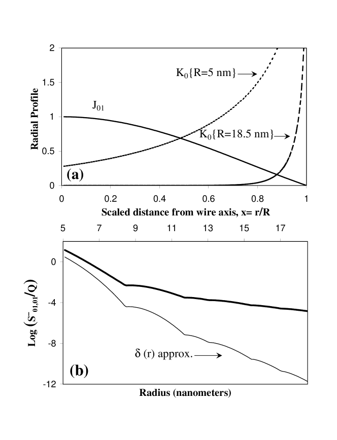
In Fig. 1(a) we plot the modified Bessel function of the second kind for the lowest channel, ; it contains the effects of the Coulomb scattering in the scattering matrix elements. In the - plane, the function is very strongly peaked along the line, therefore we specifically chose to plot . In order to see the behavior over the entire range of wire radii we present plots for the minimum radius and maximum radius that we consider. Alongside we plot the un-normalized radial profile of the carrier density in the lowest channel . We find that the overlap of the carrier density profile with the prominent region of decreases significantly with increased wire radius, indicating that an approximation that replaces the radial profile with a delta function at the wire axis would deteriorate rapidly with larger wire radius. That is exactly what we see in Fig. 1(b) where we plot the intra-band scattering matrix element for the lowest channel using first Eq. (12) which uses the appropriate radial profile and secondly Eq. (14) which uses the -function approximation. The two curves are noticeably different even for a wire radius of nm, but for larger wire radii they differ by several orders of magnitudes. This is exactly what one would expect for a surface distribution of impurities because the impurities are further removed from the wire axis for a larger wire.
Figure 2 shows the scaling of the Fermi wavevector with the radius. We see that the dimensionless product of the wire radius with the Fermi wavevector, has an almost monotonic growth with the radius. The Fermi vector itself decreases noticeably as each new channel becomes available, and then rebounds gradually but with an overall decline of the peak values reached before each succeeding channel enters. So the general trend is that gets smaller with increasing radius; with sufficiently large number of channels we expect it to approach the bulk value which, for the carrier density we have assumed, would be . Our plot suggests a gradual approach to that limit. That limit gives a criterion for when the system makes the transition from quasi-1D to 3D.
We plot the mobility in Fig. 3 on a logarithmic scale to show that the growth of the mobility with radius is of an exponential nature in between points of sharp declines. The most striking feature is that the multi channel scattering destroys the simple monotonic growth of the mobility seen with a single channel [11]. As the radius increases, and each new channel becomes energetically available for scattering there is a sharp reduction in the average mobility. In between the addition of new scattering channels, the increasing wire radius causes the mobility to grow, but that growth has an inflection point, reflecting the competition with increased scattering. The sharp declines cause an overall lowering of the mobility as the radius increases significantly. This is consistent with an eventual approach to bulk behavior.

We get a sense of the actual intrinsic magnitude of the mobility and its variations in Fig. 4 where a linear scale is employed. This figure also illustrates the effect of changing the radial scaling of the impurity density itself; we have plotted alongside the mobility for the case described in Eqs. (17) and (18) where regardless of the increased wire growth the linear density of the impurity layer remains constant. Those equations show that there is then an extra factor of in the mobility, because the surface density becomes sparser with increased wire size; this causes the mobility to increase faster at larger radii as we see from the plot. Otherwise the two curves are quite similar implying that the essential features are not affected significantly by the nature of the impurity distribution, because the strong exponential behavior of the modified Bessel functions dominates the trend.
We have assumed a simple model which highlights general trends in the carrier mobility and related parameters as a semiconductor nanowire deviates from the strict size quantization limit towards bulk behavior. Real semiconductor wires will not have a uniform cross section, and are likely to have impurities in the wire interior as well as on the surface, so the behavior we have seen will therefore likely be less sharp. Moreover it is known that screening affects intra-band scattering more significantly [16, 23] than inter-band scattering. So a more accurate treatment of the dielectric function is likely to diminish the changes in the mobility as new channels become available. But the general trends we have established are sufficiently striking that those features would be relevant in experimentally observed behavior of the mobility as the wire size is increased. In particular the effect of inter-channel scattering should be manifest in the degenerate limit.
References
References
- [1] Cui Y and Leiber C M 2001 Science 291 851
- [2] Cui Y, Zhong Z, Wang D, Wang W U and Leiber C M 2003 Nano Lett. 3 149
- [3] Ohlsson B J, Björk M T, Magnusson M H, Deppert K, Samuelson L and Wallenberg L R 2001 Appl. Phys. Lett. 79 3335
- [4] Hiruma K, Yazawa M, Haraguchi K, Ogawa K, Katsuyama T, Koguchi M and Kakibayashi H 1993 J. Appl. Phys. 74 3162
- [5] Wu Y and Yang P 2000 Chem. Mater. 12 605
- [6] Wang D, Wang Q, Javey A, Tu R, Dai H, Kim H, McIntyre P C, Krishnamohan T and Saraswat K C 2003 Appl. Phys. Lett. 83 2432
- [7] Duan X, Huang Y, Cui Y, Wang J and Leiber C M 2001 Nature 409 6
- [8] Bakkers EPAM, Van Dam JA, De Franceschi S, Kouwenhoven LP, Kaiser M, Verheijen M, Wondergem H and Van der Sluis P 2004 Nature Mater. 3 769
- [9] Thelander C, Björk M T, Larsson M W, Hansen A E, Wallenberg L R and Samuelson L 2004 Solid State Commun. 131 573
- [10] Sakaki H 1981 Jpn. J. Appl. Phys. 19 148
- [11] Lee J and Spector H N 1983 J. Appl. Phys. 54 3921
- [12] Lee J and Spector H N 1985 J. Appl. Phys. 57 366
- [13] Gold A and Ghazali A 1990 Phys. Rev. B 41 7626
- [14] Fishman G 1986 Phys. Rev. B 34 2394
- [15] DasSarma S and Xie X C 1987 Phys. Rev. B 35 9875
- [16] Weng Y and Leburton J P 1989 J. Appl. Phys. 65 4983
- [17] Manaselyan A K, Aghasyan M M and Kirakosyan A A 2002 Physica E 14 366
- [18] Sundaram V S and Mizel S 2004 J. Phys. C 16 4697
- [19] Cui Y, Lauhon L J, Gudiksen M S, and Wang J 2001 Appl. Phys. Lett. 78 2214
- [20] Holmes J D, Johnston K P, Doty R C and Korgel B A 2000 Science 287 1471
- [21] Gudisen M S and Leiber C M 2000 J. Am. Chem. Soc. 122 8801
- [22] Dingle R, Störmer H L, Gossard A C and Wiegmann W 1978 Appl. Phys. Lett. 33 665
- [23] Ferry D K and Goodnick S M Transport in Nanostructures, (Cambridge 1997)