a): Present address: ]Graduate School of Material Science, University of Hyogo, Kamigori-cho, Ako-gun, Hyogo 678-1297, Japan
b): Also at: ]Combinatorial Exploration Material Science and Technology, Tsukuba, Japan
Electron transport in ZnO thin films
Abstract
Epitaxial, n-type ZnO films grown by a laser molecular-beam epitaxy method were investigated by the temperature-dependent Hall-effect technique. The 300-K carrier concentration and mobility were about cm-3 and 440 cm2/Vs, respectively. Transport characteristics are calculated by solving the Boltzmann transport equation using a variational method. Mobility limit of 430 cm2/Vs was calculated at 300 K. The temperature dependence of the mobility for an undoped film is calculated and agrees favorably well with experimental data if physical parameters are chosen so as to approach those. In the experimental ‘mobility versus concentration’ curve, unusual phenomenon was observed, i.e., mobilities at 1018 cm-3 are significantly smaller than those at higher densities above cm-3. It is qualitatively explained in terms of electron-plasmon interaction.
pacs:
78.55.Et: 81.15.Fg: 71.35.Cc: 72.15.-vZnO is direct band gap semiconductor suitable for the development of efficient blue and UV optoelectronic devices. Attempts have extensively been made to incorporate shallow acceptor impurities in this material. We have recently developed a reliable and reproducible method to grow p-type ZnO layers, leading to the observation of electro-luminescence from a homoepitaxial p-n junction structure Tsukazaki et al. (2005). The exploit for discovering the p-type conduction has noticed us the importance of quality improvement of undoped epilayers as a starting point of reliable doping Tsukazaki et al. (2003). In this work, the electrical properties of epilayers are investigated since mobility is considered to be the figure of merit for material characterization.
Several investigators have reported the mobilities in epitaxial ZnO layers grown by various techniques Miyamoto et al. (2002); Elmer (2001); Ginley and Bright (2000); Kato et al. (2003); Iwata et al. (2000); Kaidashev et al. (2003). The room-temperature values are relatively poor compared with bulk ZnO. Our recent mobilities Tsukazaki et al. (2005) surpassed, however, the best bulk data ever reported Look et al. (1999, 1998); Rode (1975) and are significantly higher than the calculation results performed for bulk crystals by Rode (p. 49 of Ref. Rode, 1975). Since the calculated result presents the material limit Rode (1975); Albrecht et al. (1999), it needs to calculate the mobility again with a different set of parameters so as to increase its limit. The corresponding critical discussion of their choice will be made in this work.
To date, there have only been a few attempts Elmer (2001); Miyamoto et al. (2002) to model electron transport in doped ZnO. The present publication also reports carrier concentration dependence of mobility including an effect of the electron-plasmon interaction Fischetti (1991); Lowney and Bennett (1991).
Table I gives the ZnO materials parameters that are used in these transport theory calculation Lowney and Bennett (1991); Seeger (2002); Mollwo (1982). Since the current is perpendicular to the c-axis in our case Rode (1975), the piezoelectric coefficient of 0.21 was used, the definition of which is found in p. 36 of Ref. Rode, 1975. We have not adopted the relaxation time approximation for the mechanisms that involve relatively high-energy transfers, e.g., longitudinal optical phonons. The polar optical-phonon energy, , is 72 meV, and corresponding Debye temperature (837 K) by far exceeds the room temperature Mollwo (1982). The pair of and was selected from the literature as to make their difference smaller. The effective band mass was adopted instead of its polaron mass. Otherwise, the resulting mobility become smaller. Since Rode’s iterative technique takes a long time to reach its convergence Rode (1975); Fischetti (1991), the present computations are based on the variational principle method Lowney and Bennett (1991); Ruda and Lai (1990). This method allows the combination of all scattering mechanism without invoking Mattheissen’s rule.
The following electron scattering mechanisms are considered: (1) polar optical-phonon scattering, (2) ionized-impurity scattering, (3) acoustic-phonon scattering through the deformation potentials, and (4) piezo-electric interactions Seeger (2002); Lowney and Bennett (1991); Ruda and Lai (1990). The final expression used is as follows Lowney and Bennett (1991):
| (1) |
The terms and refer to the low- and high-frequency dielectric constants, respectively. m∗ refers to the electron effective mass in units of the free electron mass in rest. T refers to the temperature, and is the reduced polar optical phonon energy defined as . is the half-integral Fermi-Dirac integral and is the reduced Fermi energy given in thermal units. The terms and are defined and explained in Ref. Lowney and Bennett, 1991.
All films were grown on insulating and lattice-matched ScAlMgO4 (SCAM) substrates by laser molecular-beam epitaxy. ZnO single-crystal and (Ga,Zn)O ceramics targets were ablated by excimer laser pulses with an oxygen flow of torr. We have grown them at about 1000 ∘C with introduction of semi-insulating (Mg, Zn)O buffer layers. The detailed description of fabrication methods has been given elsewhere Ohtomo and Tsukazaki (2005); Makino et al. (2005). The films were patterned into Hall-bars and the contact metal electrodes were made with Au/Ti for n-type film, giving good ohmic contact. Carrier concentrations and Hall mobilities were measured at various temperatures.
Figure 1 shows temperature dependence of mobility () for an undoped ZnO film and for a bulk crystal by closed and open circles. The values of are 440 cm2/Vs and 5,000 cm2/Vs at 300 and 100 K, respectively. Below 100 K, the distribution of activated carriers in this sample is too sparse to detect the sizable Hall electromotive force. We did not observe abnormal temperature dependence requiring a so-called two-layer analysis in these data Look and Molnar (1997). It thus suggests the negligible contribution from a degenerate interfacial layer to our samples probably because ours were grown on lattice-matched substrates.
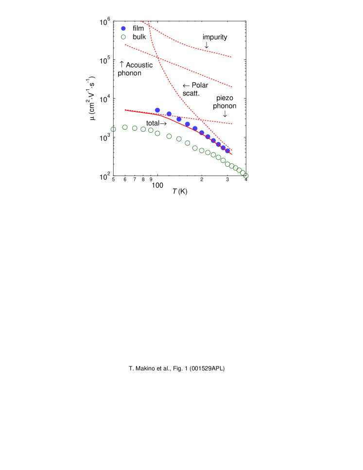
We have derived partial mobilities by accounting for respective scattering mechanisms in the nondegenerate (undoped) limit. The results are given in Fig. 1 as a function of temperature by dashed lines. The curve for ionized impurity scattering are calculated assuming that the material is uncompensated and concentration being equal to . The carrier concentration data have been given elsewhere Tsukazaki et al. (2005); data were fitted with activation energies of 30 and 60 meV. The total electron mobility calculated by combining all of the partial scattering mechanisms is also given by a solid line. The relative importance of the various scattering mechanisms mimics that found in ZnS Ruda and Lai (1990). For example, the polar optical phonon scattering at higher temperatures controls inherent mobility limit curve. At low temperatures (down to 100 K) on the other hand, piezoelectric phonon interaction is the dominant scattering mechanism. Our experimental data are in reasonably good agreement with theory. The mobility limit at 300 K is about 430 cm2/Vs. The probable discrepancy between them is because our model calculates drift mobility, while experimental results correspond to Hall mobility. The theoretical Hall factor was given in Ref. Rode, 1975.
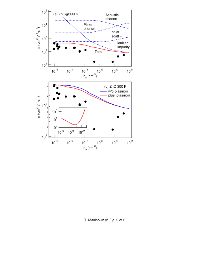
On the other hand, the situation is somewhat different for the cases of Ga-doped n-type films Makino et al. (2004). Figure 2(a) shows 300-K experimental mobilities plotted against carrier concentration. The mobilities of doped films are significantly smaller than those of undoped one Makino et al. (2002a, b). Obviously, this tendency can be qualitatively attributed to the increased density of impurities. For quantitative comparison, partial mobilities are calculated and given in Fig. 2(a) by dashed lines. We have taken the effects of screening for both ionized impurities and polar optical phonon scattering into account. Polar interactions reflecting the ionicity of the lattice are dominant in scattering mechanism, while, at heavier doping levels, ionized impurity scattering controls the inherent mobility limit curve Ruda and Lai (1990); Lowney and Bennett (1991). The experimental data agree well with our calculation (solid curve) except for the intermediate concentration range. Particularly, our model could not reproduce a relative minimum in the “ versus ” curve, which has been experimentally observed in this intermediate doping range. The situation at > 1020 cm-3 could be improved probably if the effects of non-parabolic band structure as well as of clustering of charged carriers would be taken into account Elmer (2001), which is beyond the scope of our work.
Fischetti Fischetti (1991) and Lowney and Bennett Lowney and Bennett (1991) obtained theoretical curve having a “dip” in the intermediate concentrations by including a higher-order effect, i.e., plasmon scattering. Plasmons are the collective excitations of free electrons against the background charges. It has been shown that if decay due to collisional damping dominates over Landau damping, the electron-plasmon scattering can reduce somewhat the mobility for electron concentrations greater than 1017 cm-3. The coupling of the plasmon to the polar optical-phonon modes have been neglected because there is no sufficiently tractable theory for the hybrid modes, and because such coupling should not have much of an effect on the overall numerical results for the mobility. We thus decide to deal with the pure uncoupled modes throughout.
The momentum relaxation time for an electron to absorb or emit a plasmon of energy is given by;
| (2) |
where upper and lower signs represent absorption and emission, respectively. , is the plasmon cut-off wavenumber, above which plasma oscillation cannot be sustained. The cut-off wavenumber is on the order of the inverse Thomas-Fermi screening length defined elsewhere Lowney and Bennett (1991). , and is the Bose occupation number of plasmons and . The relaxation time approximation was adopted here because it is valid for the entire concentration range of interest according to Ref. Fischetti, 1991.
The dependence of the cut-off wavenumber and plasma frequency on doping density leads to interesting phenomena for plasmon scattering such as a relative minimum in mobility as a function of concentration. Figure 2(b) shows the effect of electron-plasmon interaction on the mobility. The uppermost curve is drawn without including this effect, while the next one takes it into account. Notice, in particular, the “dip” is at 1018 cm-3. The partial mobility is shown in the inset. Our theory thus describes a rise due to the increase in the plasmon frequency at these doping levels as has been observed experimentally, although there is poor quantitative agreement between theory and experiment. We propose that more experiments using further optimized samples be done in this doping range to determine if the tendency on mobility agrees not only qualitatively but also quantitatively.
In summary, electron transport characteristics of ZnO are experimentally studied and calculated by solving the Boltzmann transport equation exactly for all major scattering mechanisms. The polar optical phonon and ionized impurity electron scattering mechanisms are properly screened in this treatment. Temperature dependence of the mobility is investigated for nondegenerate samples, and compare with our experimental data. Reasonable agreement between experimental data and theory was found. Mobility limits are derived for this material as 430 cm2/Vs at 300 K. Electron mobility was also calculated as a function of carrier concentration. Even if we take the effect of electron-plasmon interaction into consideration, our experimental mobilities for doped films are significantly lower than theoretical values especially for the concentration range around 1019 cm-3.
Acknowledgement — One of the authors (T. M.) thanks H. S. Bennett of NIST, D. L. Rode of Washington University, St. Louis, H. Ruda of University of Toronto, Canada, and B. Sanborn of Arizona State University for helpful discussions. Thanks are also due to Shin Yoshida for technical assistance during our experiments.
References
- Tsukazaki et al. (2005) A. Tsukazaki, A. Ohtomo, T. Onuma, M. Ohtani, T. Makino, M. Sumiya, K. Ohtani, S. F. Chichibu, S. Fuke, Y. Segawa, et al., Nature Materials 4, 42 (2005).
- Tsukazaki et al. (2003) A. Tsukazaki, A. Ohtomo, M. Kawasaki, C. H. Chia, T. Makino, Y. Segawa, T. Koida, S. Chichibu, and H. Koinuma, Appl. Phys. Lett. 83, 2784 (2003).
- Miyamoto et al. (2002) K. Miyamoto, M. Sano, H. Kato, and T. Yao, Jpn. J. Appl. Phys. 41, L1203 (2002).
- Elmer (2001) K. Elmer, J. Phys. D. 34, 3097 (2001).
- Ginley and Bright (2000) D. S. Ginley and C. Bright, MRS Bull. 25, 15 (2000).
- Kato et al. (2003) H. Kato, M. Sano, K. Miyamoto, and T. Yao, Jpn. J. Appl. Phys. 42, 2241 (2003).
- Iwata et al. (2000) K. Iwata, P. Fons, S. Niki, A. Yamada, K. Matsubara, K. Nakahara, and H. Takasu, Phys. Status Solidi (a) 180, 287 (2000).
- Kaidashev et al. (2003) E. M. Kaidashev, M. Lorenz, H. von Wenckstern, A. Rahm, H.-C. Semmelhack, K.-H. Han, G. Benndorf, C. Bundesmann, H. Hochmuth, and M. Grundmann, Appl. Phys. Lett. 82, 3901 (2003).
- Look et al. (1999) D. C. Look, J. W. Hemsky, and J. R. Sizelove, Phys. Rev. Lett. 82, 2552 (1999).
- Look et al. (1998) D. C. Look, D. C. Reynolds, J. R. Sizelove, R. L. Jones, C. W. Litton, G. Cantwell, and W. C. Harsch, Solid State Commun. 105, 399 (1998).
- Rode (1975) D. L. Rode, Semiconductors and Semimetals 10, 1 (1975).
- Albrecht et al. (1999) J. D. Albrecht, P. P. Ruden, S. Limpijumnong, W. R. L. Lambrecht, and K. F. Brennan, J. Appl. Phys. 86, 6864 (1999).
- Fischetti (1991) M. V. Fischetti, Phys. Rev. B 44, 5527 (1991).
- Lowney and Bennett (1991) J. R. Lowney and H. S. Bennett, J. Appl. Phys. 69, 7102 (1991).
- Seeger (2002) K. Seeger, Semiconductor Physics: An Introduction (Springer Verlag, Berlin, 2002), 8th ed.
- Mollwo (1982) E. Mollwo, in Semiconductors: Physics of II-VI and I-VII Compounds, Semimagnetic Semiconductors, edited by O. Madelung, M. Schulz, and H. Weiss (Springer, Berlin, 1982), vol. 17 of Landolt-Börnstein New Series, p. 35.
- Ruda and Lai (1990) H. E. Ruda and B. Lai, J. Appl. Phys. 68, 1714 (1990).
- Ohtomo and Tsukazaki (2005) A. Ohtomo and A. Tsukazaki, Semicond. Sci. & Technol. 20, S1 (2005).
- Makino et al. (2005) T. Makino, Y. Segawa, M. Kawasaki, and H. Koinuma, Semicond. Sci. & Technol. 20, S78 (2005).
- Look and Molnar (1997) D. C. Look and R. J. Molnar, Appl. Phys. Lett. 70, 3377 (1997).
- Makino et al. (2004) T. Makino, Y. Segawa, A. Tsukazaki, A. Ohtomo, S. Yoshida, and M. Kawasaki, Appl. Phys. Lett. 85, 759 (2004).
- Makino et al. (2002a) T. Makino, C. H. Chia, Y. Segawa, A. Ohtomo, K. Tamura, M. Kawasaki, and H. Koinuma, Phys. Status Solidi (b) 299, 853 (2002a).
- Makino et al. (2002b) T. Makino, K. Tamura, C. H. Chia, Y. Segawa, M. Kawasaki, A. Ohtomo, and H. Koinuma, Phys. Rev. B 65, 121201(R) (2002b).
| Parameter | Symbol | Value |
|---|---|---|
| Energy gap (300 K) | Eg (eV) | 3.37 |
| Electron effective mass | m∗ () | 0.24 |
| High-freq. dielectric constant | 8.1 | |
| Static dielectric constant | 4.0 | |
| Optical phonon energy | (meV) | 72 |
| Acoustic deformation potential | (eV) | 3.8 |
| Longitudinal elastic constant | (107 dyn/cm2) | 2.05 |
| Piezoelectric coefficient | 0.21 |