Polarization Relaxation Induced by Depolarization Field in Ultrathin Ferroelectric BaTiO3 Capacitors
Abstract
Time-dependent polarization relaxation behaviors induced by a depolarization field were investigated on high-quality ultrathin SrRuO3/BaTiO3/SrRuO3 capacitors. The values were determined experimentally from an applied external field to stop the net polarization relaxation. These values agree with those from the electrostatic calculations, demonstrating that a large inside the ultrathin ferroelectric layer could cause severe polarization relaxation. For numerous ferroelectric devices of capacitor configuration, this effect will set a stricter size limit than the critical thickness issue.
pacs:
77.22.Ej, 77.22.Gm, 77.80.Dj, 77.55.+fWith recent breakthroughs in fabricating high-quality oxide films Ahn ; YSKim1 ; HNLee , ultrathin ferroelectric (FE) films have attracted much attention from the scientific as well as application points of view. As the FE film thickness approaches tens of unit cell length, the FE films often show significantly different physical properties from those of bulk FE materials. Some extrinsic effects, especially coming from FE film surfaces and/or interfaces with other materials, could be very important Shaw . For some other cases, intrinsic physical quantities could play vital roles in determining the unique properties of ultrathin films.
Many FE-based electronic devices have the capacitor configuration, where a FE layer is inserted between two conducting electrodes. Then, polarization bound charges will be induced at the surfaces of the FE layer, but compensated by free charge carriers in the conducting electrodes. In real conducting electrodes, however, the compensating charges will be induced with a finite extent, called the screening length . This will result in an incomplete compensation of the polarization charges. Such an incomplete charge compensation should induce a depolarization field inside the FE layer, with a direction opposite to that of the FE polarization Mehta . Therefore, will appear in every FE capacitor, and its effects will becomes larger with the decrease of Mehta . (For a FE film without electrodes, there is no compensation for the polarization bound charge, so the value of will become even larger than that of the FE capacitor case.) has been known to be important in determining the critical thickness Junquera and domain structure of ultrathin FE films Kornev ; Wu ; Fong , and reliability problems of numerous FE devices Kang1 ; Kang2 .
Recently, using a first principles calculation, Junquera and Ghosez investigated the critical thickness of BaTiO3 (BTO) layers in SrRuO3(SRO)/BTO/SRO capacitor Junquera . For calculations, they assumed that all of the BTO and SRO layers were fully strained with the SrTiO3 substrate. By taking the real SRO/BTO interfaces into account properly, they showed that could make the ferroelectricity vanish for the BTO films thinner than 6 unit cells, i.e. 2.4 nm Junquera . More recently, using pulsed laser deposition with a reflection high energy electron diffraction monitoring system, we fabricated high-quality fully-strained SRO/BTO/SRO capacitors on SrTiO3 substrates with between 5 and 30 nm YSKim1 ; YSKim2 . With a very low leakage current, we could directly measure their - hysteresis loops YSKim1 . In this letter, we report the time-dependent polarization changes of the ultrathin BTO films. We find that the net of the ultrathin BTO films decreases quite rapidly in time. We will show that the relaxation should originate from . By compensating for with an external potential, we can determine the values of the SRO/BTO/SRO capacitors experimentally. These measured values agree with the values from the electrostatic calculations. Finally, we will discuss the effect of the relaxation on a practical size limitation imposed on actual FE devices.
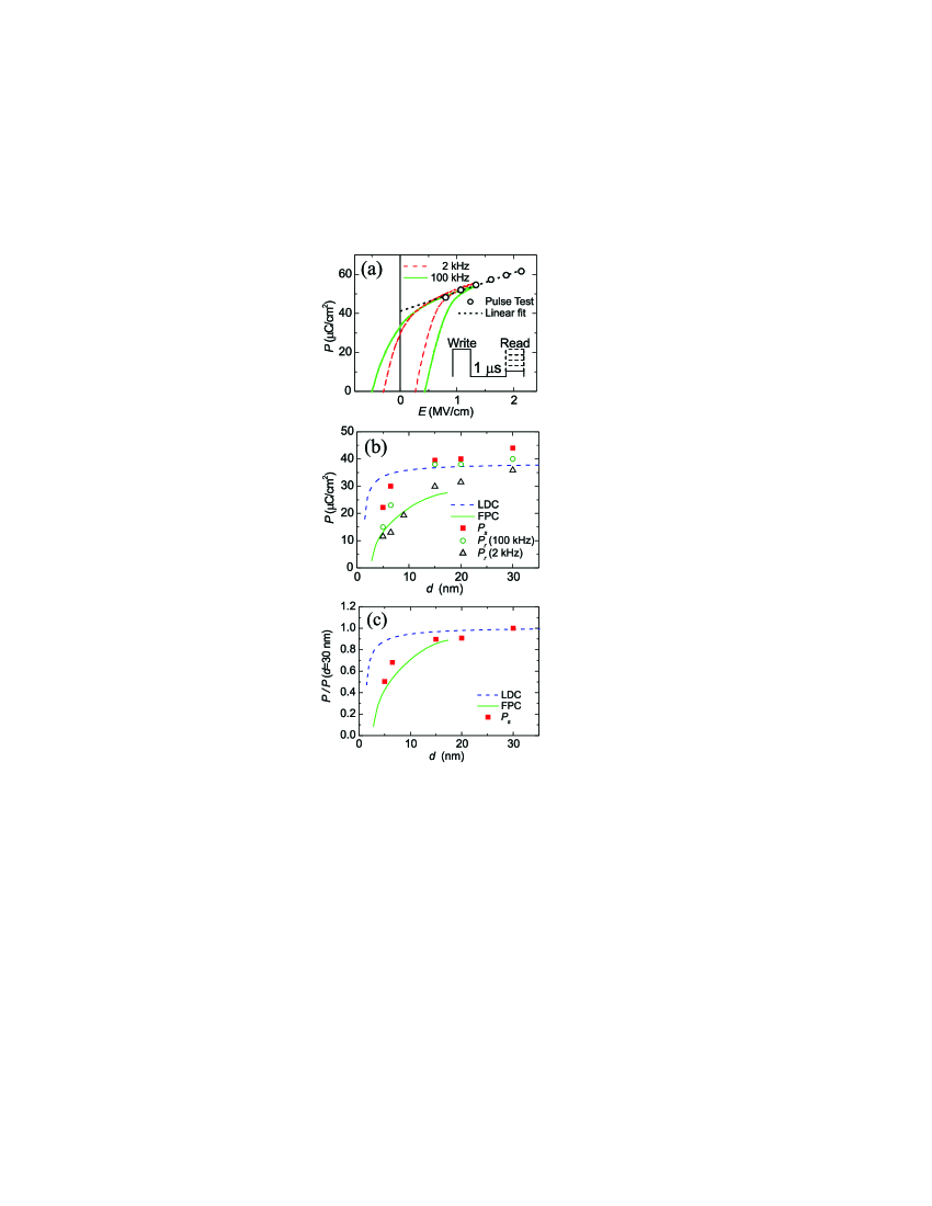
In our earlier report YSKim1 , we obtained the thickness-dependent remnant polarization values from the - hysteresis loops, measured at 2 kHz in ultrathin FE films as thin as 5 30 nm. With further studies on the frequency dependence of the values in - hysteresis loops, as shown in Fig. 1(a) for a 15 nm thick BTO capacitor, we found differences in the values when the measuring frequency is varied. These results suggest that the FE domain dynamics should play an important role for ultrathin FE films, where the FE domain wall motion is known to be strongly suppressed Tybell . Note that the first principles calculation (FPC) and the Landau-Devonshire calculation (LDC) do not consider the domain dynamics, so their predicted polarization values should be called as spontaneous polarization .
Since the value significantly affects the subsequent analysis of relaxation, precise determination of values is necessary. To determine the precise values of , we applied pulse trains, which are schematically shown in the inset of Fig. 1(a) Smolenskii . The interval between write and read pulses was set to 1 s to minimize the effects of the relaxation, and the current responses under the read pulse were measured. The total amount of charge is obtained by integrating the current responses in time. The read pulses with different heights were used to obtain the linear part of the polarization under an external electric field The values can be obtained by extrapolating the linear part of the polarization to zero electric field. The triangles (black) and circles (green) in Fig. 1(b) show the values measured at 2 and 100 kHz, respectively. Also, the squares (red) show the values from the pulse test. The solid (green) and dashed (blue) curves show the theoretical predictions from the FPC Junquera and the LDC Pertsev , respectively, which take account of . Note that neither of these theories can explain the thickness-dependence of quantitatively. However, it is known that the FPC predicts systematically somewhat lower bulk lattice constants compared to real values, so the compressive stress predicted by the FPC could be smaller than that in the fully strained sample, resulting in a smaller . To avoid this systematic error, we normalized the polarization values to those of a 30 nm thick BTO capacitor. We found that the thickness-dependent scaling of also follows the FPC predictions quite well, as shown in Fig. 1(c).
The large difference in values between the 2 and the 100 kHz tests indicates that there should be a strong change in the net between 10 and 500 s. Time-dependent changes were investigated by applying two kinds of pulse trains, as shown in the inset of Fig. 2(a). For the write and the read pulses with the same (opposite) polarities, the amount of nonswitching (switching) can be determined Kang1 . The difference , between the switching and the nonswitching should be twice as large as the net . As shown in Fig. 2(a), decreases quite rapidly for the film with = 15 nm; falls to less than of the value within a relaxation time of 1000 s. As shown with the solid squares (black) in Fig. 2(b), decay follows a power-law dependence on . Similar power-law decays of were observed for all the BTO films in the thickness range of 5 30 nm. Note that such a strong polarization relaxation could pose a serious problem in capacitor-type ultrathin FE devices.
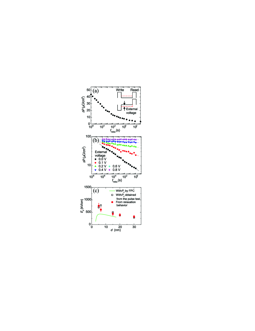
What is the origin of such strong polarization relaxations? We thought that they could be closely related to large induced inside the BTO films. To verify this idea, we slowed down the relaxation phenomena by applying an external voltage, as shown in the inset of Fig. 2(a). The values of the applied external electric field were obtained by dividing the applied external voltage by the corresponding film thickness. When the external field is applied in the opposite direction of , the potential gradient inside the FE layer will decrease. Figure 2(b) shows that the slope of the power-law decay becomes smaller, as increases. Assuming that the depth of the double-well potential for BTO ferroelectricity can be considered negligible compared to the effect of , we approximately determined experimental values from the applied electric field under which the slope becomes zero. Since is proportional to , the value should increase slightly on application of . After correcting this minor contribution, we could determine the values, which are plotted as solid circles (red) in Fig. 2(c).
From electrostatic calculations on the capacitor geometry, Mehta et al. showed that
| (1) |
where is the thickness of the FE layer, and and are the relative dielectric constants of the FE layer and the electrode, respectively Mehta . To obtain theoretical values for our SRO/BTO/SRO capacitors, we have to know accurate values of , , and . Unfortunately, the reported physical parameter values in the literature vary Mehta ; Junquera ; Black ; Dawber . Also, we could not find any definite experimental study on .
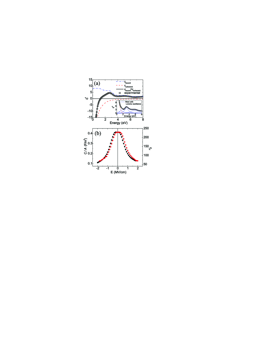
To obtain the value of for an SRO electrode, we used optical spectroscopy. We measured the optical reflectivity spectra of epitaxial SrRuO3 films (thickness: about 0.5 m) in a wide frequency region between 5 meV and 30 eV and performed a Kramers-Kronig analysis to obtain the frequency-dependent dielectric function, [=)]. The details of these measurements and analysis were published elsewhere JSLee1 ; JSLee2 . The open squares in Fig. 3(a) and the inset show experimental values of and , respectively. Note that in Eq. (1) represents the dielectric response from the bound charges, namely bound electrons and phonons. Since SRO is metallic, there should be a large contribution from the free Drude carriers, which masks the dielectric response from the bound charges. To obtain , we decompose into a free carrier contribution and a bound electron contribution by fitting the experimental with a series of Lorentz oscillators, which are displayed as the dotted (blue) lines in the inset of Fig. 3(a). The dash-dotted (blue) lines indicate the bound electron contribution. From the dc limit of , we could estimate that the bound electron contribution to is about 8.17. The phonon contribution to was evaluated in a similar way by analyzing the phonon spectra and found to be about 0.28 JSLee1 . Consequently, is determined to be about 8.45.
Using the carrier density cm3 of SRO Shepard , the experimental value of , and the effective mass of an electron , where is the mass of a free electron Cao ; Okamoto , we applied the free electron model and obtained Å Mehta ; Kittel . We also measured from the capacitance-electric field - curves of BTO capacitors. Figure 3(b) shows the - curve for the 5 nm BTO capacitor. The - curve has the hysteretic behavior typical for a FE capacitor. The BTO capacitors with 5 30 nm thickness show almost the same - curves. The values can vary from 70 to 230 depending on the applied . Since most of our experiments were performed under a finite applied field, which corresponds to a value between 1 and 2 MV/cm, the were estimated to be about 80 interface .
With the measured values of , , and , we could estimate the theoretical values from Eq. (1) with the values obtained from the pulse test. The open squares in Fig. 2(c) are the theoretical values. The solid (green) line shows the theoretical values with the values, obtained from the FPC. These theoretical values from the electrostatic model agree quite well with the experimental values, determined from the polarization relaxation. It should be noted that the values are comparable with or even larger than the measured coercive fields (in our samples, 300 400 kV/cm). These large values can cause reversal and FE domain formation, which will result in a reduction of the net value as time elapses. The fact that two independent determinations provided nearly the same values demonstrates that the polarization relaxation behavior should be dominated by inside the FE layer.
Note that the -induced decay comes intrinsically from the incomplete compensation of the charges (due to the finite screening length of the electrodes) in real conducting electrode, so that it will inevitably pose a fundamental limit for most FE device applications using the capacitor configuration. This limitation should be much more severe than that due to the critical thickness of the FE ultrathin films Junquera . Even if the FE film is thicker than the critical thickness, it is feasible that the -induced decay is large enough to make the net decrease significantly, resulting in retention failures for numerous FE devices. As decreases, increases significantly. With the current miniaturization trends in some FE devices, the large value of should play a very important role in determining the ultimate size limits of FE devices.
In order to reduce device failure due to the polarization relaxation, we can try to select better electrode and FE materials. Noble metals, such as Pt, have been considered better electrodes because they have high carrier density (resulting in values smaller than that of SRO). However, the values of typical noble metals are much smaller than that of SRO, i.e. 8.45 Ehrenreich , so in capacitors with noble metal electrodes can be large. For example, in the range of 500 900 kV/cm is expected for a 15 nm thick BTO film with noble metal electrodes (typically, Å, ). Thus, the -induced relaxation for the ultrathin BTO capacitors with the noble metal electrodes could be at least equal to or worse than that with SRO electrodes. Proper FE material selection can be another option. Since PbTiO3 is known to have a much deeper double-well potential than that of BTO Pertsev ; Cohen , the relaxation should occur at a much lower rate even with the same value of . Optimization of FE materials should be of great importance for the improvement of ultrathin film nanoscale FE device performances.
In summary, we demonstrated that the depolarization field inside the ferroelectric film could cause a severe polarization relaxation. By slowing down the relaxation under an external field, we could determine the depolarization field in a real capacitor of ultrathin SrRuO3/BaTiO3/SrRuO3 experimentally, which result is in good agreement with electrostatic calculations. Our investigation demonstrates that the depolarization field originates from intrinsic properties of electrode material such as the finite screening length and that the depolarization field should play an important role in domain dynamics in ultrathin FE films. The polarization relaxation due to the depolarization field could pose a serious size limitation for ultrathin ferroelectric devices.
The authors thank Prof. Sug-Bong Choe in Seoul National University for valuable discussions. This work was financially supported by the Korean Ministry of Science and Technology through the Creative Research Initiative program and by KOSEF through CSCMR.
References
- (1) C. H. Ahn, K. M. Rabe, and J.-M. Triscone, Science 303, 488 (2004).
- (2) Y. S. Kim, D. H. Kim, J. D. Kim, Y. J. Chang, T. W. Noh, J. H. Kong, K. Char, Y. D. Park, S. D. Bu, J.-G. Yoon, and J.-S. Chung, Appl. Phys. Lett. 86, 102907 (2005).
- (3) H. N. Lee, H. M. Christen, M. F. Chisholm, C. M. Rouleau, and D. H. Lowndes, Nature 433, 395 (2005).
- (4) T. W. Shaw, S. Trolier-McKinstry, and P. C. McIntyre, Annu. Rev. Mater. Sci. 30, 263 (2000).
- (5) B. B. Mehta, B. D. Silverman, and J. T. Jacobs, J. Appl. Phys. 44, 3379 (1973).
- (6) J. Junquera and P. Ghosez, Nature 442, 506 (2003).
- (7) I. Kornev, H. Fu, and L. Bellaiche, Phys. Rev. Lett. 93, 196104 (2004).
- (8) Z. Wu, N. Huang, Z. Liu, J. Wu, W. Duan, B.-L. Gu, and X.-W. Zhang, Phys. Rev. B 70, 104108 (2004).
- (9) D. D. Fong, G. B. Stephenson, S. K. Streiffer, J. A. Eastman, O. Auciello, P. H. Fuoss, and C. Thompson, Science 304, 1650 (2004).
- (10) B. S. Kang, J.-G. Yoon, T. W. Noh, T. K. Song, S. Seo, Y. K. Lee, and J. K. Lee, Appl. Phys. Lett. 82, 248 (2003).
- (11) B. S. Kang, J.-G. Yoon, D. J. Kim, T. W. Noh, T. K. Song, Y. K. Lee, J. K. Lee, and Y. S. Park, Appl. Phys. Lett. 82, 2124 (2003).
- (12) Y. S. Kim, J. Y. Jo, D. J. Kim, Y. J. Chang, J. H. Lee, T. W. Noh, T. K. Song, J.-G. Yoon, J.-S. Chung, S. I. Baik, Y.-W. Kim, and C. U. Jung, cond-mat/0506495 (2005).
- (13) T. Tybell, P. Paruch, T. Giamarchi, and J.-M. Triscone, Phys. Rev. Lett. 89, 097601 (2002).
- (14) G. A. Smolenskii, V. A. Bokov, V. A. Isupov, N. N. Krainik, R. E. Pasynkov, and A. I. Sokolov, Ferroelectrics and Related Materials (Gordon and Breach, New York, 1984) pp4-5.
- (15) N. A. Pertsev, A. G. Zembilgotov, and A. K. Tagantsev, Phys. Rev. Lett. 80, 1988 (1998).
- (16) C. T. Black and J. J. Welser, IEEE Trans. Electron Devices 46, 776 (1999).
- (17) M. Dawber, P. Chandra, P. B. Littlewood, and J. F. Scott, J. Phys.: Condens. Matter 15, L393 (2003).
- (18) J. S. Lee, Y. S. Lee, T. W. Noh, S. Nakatsuji, H. Fukazawa, R. S. Perry, Y. Maeno, Y. Yoshida, S. I. Ikeda, J. Yu, and C. B. Eom, Phys. Rev. B 70, 085103 (2004).
- (19) J. S. Lee, Y. S. Lee, T. W. Noh, K.Char, J. Park, S.-J. Oh, J.-H. Park, C. B. Eom, T. Takeda, and R. Kanno, Phys. Rev. B 64, 245107 (2001).
- (20) M. Shepard, S. McCall, G. Cao, and J. E. Crow, J. Appl. Phys. 81, 4978 (1997).
- (21) G. Cao, S. McCall, M. Shepard, J. E. Crow, and R. P. Guertin, Phys. Rev. B 56, 321 (1997).
- (22) J. Okamoto, T. Mizokawa, A. Fujimori, I. Hase, M. Nohara, H. Takagi, Y. Takeda, and M. Takano, Phys. Rev. B 60, 2281 (1999).
- (23) C. Kittel, Introduction to Solid State Physics, 6th ed. (John Wiley & Sons, Inc., New York, 1996) pp280-282.
- (24) Note that the charge compensation in the finite screening length in electrodes might result in space charge capacitance in series with ferroelectric capacitance. For the case of the 5 nm thick film, should be increased to 112 from 80 with the correction. However, this increase of does not change so much; from 708 to 650 kV/cm (about 8%). Because this is the most serious case, corrections are not necessary for thicker films.
- (25) H. Ehrenreich and H. R. Phillipp, Phys. Rev. 128, 1622 (1962).
- (26) R. E. Cohen, Nature 358, 136 (1992).