Half-metallic ferromagnets for magnetic tunnel junctions
Abstract
Using theoretical arguments, we show that, in order to exploit half-metallic ferromagnets in tunneling magnetoresistance (TMR) junctions, it is crucial to eliminate interface states at the Fermi level within the half-metallic gap; contrary to this, no such problem arises in giant magnetoresistance elements. Moreover, based on an a priori understanding of the electronic structure, we propose an antiferromagnetically coupled TMR element, in which interface states are eliminated, as a paradigm of materials design from first principles. Our conclusions are supported by ab-initio calculations.
pacs:
75.70.Cn,73.20.-r,85.75.-dHalf-metallic ferromagnets are ferromagnetic materials showing, in the ideal case, 100% spin polarization at the Fermi level , due to a metallic density of states in one spin direction (usually majority spin) combined with a band gap in the other spin direction (usually minority spin). First discovered by ab-initio calculations by de Groot et al. deGroot83 , these materials have drawn strong attention because of their potential applications in the field of spintronics. In principle, half-metallic ferromagnets are ideal spin injectors and detectors, because under moderate voltage they can carry current in only one spin direction. Therefore, they also constitute ideal components for Giant Magnetoresistant (GMR) and Tunneling Magnetoresistant (TMR) devices, with two half-metallic leads sandwiching a nonmagnetic normal metal spacer (in GMR) or a semiconductor or insulator spacer (in TMR). There is, for instance, the experimental result of Bowen and collaborators Bowen03 who obtained a TMR ratio (relative change of resistance upon change of the magnetization alignment of the leads) higher than 1800% in a La2/3Sr1/3MnO/SrTiO3/La2/3Sr1/3MnO junction; this extreme value was attributed to the half-metallicity of La2/3Sr1/3MnO. Motivated by such findings, we set forth to gain theoretical understanding of the conditions under which half-metals can be fully exploited in TMR devices.
The purpose of this article is twofold. First, we demonstrate by theoretical arguments on the electronic structure that it is much easier to exploit the half-metallic property in a GMR element than in a TMR one. We explain the implications caused by interface states in TMR elements, and we suggest cases of improved TMR elements without interface states. Then, we propose an antiferromagnetically coupled TMR element (to serve as a magnetic field sensor) based on an a priori understanding of the exchange interactions in such systems, as a paradigm of materials design from first principles.
The idea of using half-metals in GMR and TMR junctions seems simple. In a parallel (P) alignment of the magnetic moments of the half-metallic leads sandwiching the spacer, some current will pass, either by metallic conduction (in GMR) or by tunneling (in TMR) of majority spin electrons. On orienting the moments of the leads in an antiparallel (AP) way, for one spin channel no current can enter the junction (due to the minority-spin gap of the one lead), while in the other spin direction no current can exit the junction (due to the minority-spin gap of the other lead); thus no current can pass. Hence this is an ideal spin-controlled switch.
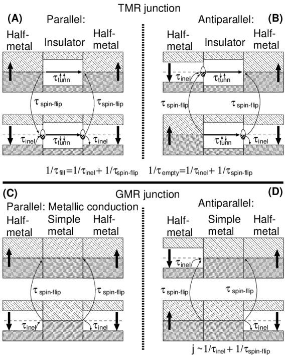
However, in TMR junctions a difficulty arises in the presence of interface states around in the half-metallic gap at the metal-insulator contact. Consider, for instance, the TMR junction in Fig. 1 (A and B), where the bands are shown schematically along the junction. Panel A shows the band alignment for both spin directions for a P alignment of the magnetzation of the half-metallic leads, while panel B shows the same for an AP alignment. At the interfaces, for the minority-spin direction, possible localized interface states are shown. If they exist, it is inevitable that they are coupled to the bulk states of the half-metal, and thus they can be important for the transport properties and for the TMR ratio of the junction, as we will now discuss.
If interface states are present, they contribute to the tunneling current . The current is controlled by two sequential processes: (i) by the tunneling itself, characterized by a rate , and (ii) by re-filling the interface states after an electron has tunneled out of them, with a characteristic rate of (or by emptying these states after an electron has tunneled into them, with a rate of ) (otherwise they are blocked by the Pauli principle or by Coulomb blockade effects). Since these processes take place sequentially, the characteristic times and must be additive. Then, in the AP alignment the current has a non-zero value, and expression for has the form (see also Fig. 1B)
| (1) |
The first term refers to filling a spin-down interface state at the left lead in Fig. 1B (up) and tunneling to the right lead, while the second term refers to tunneling from the spin-up continuum of the left lead in Fig. 1B (down) into the interface state of the right lead, and then emptying it. We distinguish among four different tunneling times, for the four different cases of tunneling between majority and minority states as shown in Fig. 1 A and B. We we name these , , , and . Evidently the slower of the two processes (i) and (ii) determines the current. If, in comparison to the slow tunneling rate, the states are immediately refilled (or emptied) after a tunneling event (we will argue below that this is expected), then and is determined by the tunneling rate alone, irrespectively of the half-metallic band gap. Similar considerations hold for the minority-spin current in the P case.
What determines the coupling of the interface states with the bulk and thus the characteristic times and ? On one hand, there are inelastic processes contributing with a rate . These can be of thermal nature or quantum fluctuations (scattering of electrons with phonons, magnons, other electrons etc.). Usually inelastic processes are slow at low temperatures, but if the Fermi level is in the proximity of the band edges, rather than in mid-gap, they can be of significance. More importantly, there is always some spin-orbit coupling present. Therefore even in the bulk of the half-metal the polarization at , , is always lower than the ideal 100%; e.g., for NiMnSb Mavropoulos04 , and the value decreases when the material is composed by heavier elements or when is touching the band edges (e.g., for PtMnSb) Mavropoulos04 . Spin-orbit coupling will contribute to filling or emptying the interface states with a rate of . This acts in parallel with the inelastic processes, and thus
| (2) |
Additional factors can come into this equation in the presence of defects or impurities which reduce by introducing gap states. For majority electrons we do not discuss the interface states separately than the bulk states, since they are irrelevant for the half-metallic property; their effect is included in .
Although the rate in Eq. (2) is low, we recall that tunneling can be a very slow process ( is long, growing exponentially with insulator thickness and barrier height). Therefore, for thick or high insulating barriers the interface states are immediately re-filled (or re-emptied) after each tunneling event, and they act as a reservoir of electrons. The fact that they are much weaker coupled to the bulk than the majority-spin states does not help, since everything is determined by the much slower tunneling time. Assuming then that all tunneling times are long, Eqs. (1) and (2) lead to
| (3) |
This means, that the current depends only on the tunneling rates for the two spin directions and not at all on the half-metallic property of the lead.
The tunneling rates themselves depend on numerous factors: the insulating barrier thickness, the details of the interface structure, the presence of interface disorder, the symmetry character of the interface states, the presence of defects in the insulating spacer, etc.. Particularly important is the spin polarization at the interface Kammerer04 . This, in the absence of interface states, is approximately the same as in the bulk of the half-metal, but in their presence it can have a completely different value and can even be reversed Galanakis04 . The influence of these factors is in general different on each of the four tunneling times , , , and , since the nature of the states involved is different. Thus some TMR ratio can appear, but no extraordinary effect can be guaranteed by the half-metallic property, unless one can eliminate the interface states. We note that if these are eliminated, there is still a low rate of incoming minority-spin states from the bulk to the interface, because of the spin-orbit coupling. This rate, however, is very low (determined by the high polarization ).
In GMR junctions, on the other hand, the interface states play no significant role, as demonstrated schematically in Fig. 1 C and D. In the P case the conduction is metallic, while in the AP case it is confined at most to the value of the spin polarization at in the bulk of the half-metallic leads (plus inelastic effects); if this is determined by the spin-orbit coupling, it should lead to an effect of the order of 1%. This means that the half-metallic property is fully exploited in the case of GMR, in contrast to TMR.
At this point we conclude that, in order to exploit the half-metallic property in TMR junctions, we must find half-metal / insulator interfaces without interface states; and to this we now turn.
The most studied half-metallic ferromagnets are probably Heusler alloys. The bulk band structure and the origin of the gap are well understood Galanakis02a , and so are their surface Galanakis02c and interface Galanakis04 properties. Unfortunately, calculations of Heusler alloy / semiconductor interfaces are conclusive on the appearance of interface states at in almost all cases. Thus, our previous analysis rules out Heusler alloys as good candidates for TMR junctions.
On the other hand, the class of half-metallic zinc-blende pnictides and chalcogenides shows no interface states at when brought in contact with zinc-blende (zb) semiconductors Mavropoulos04b . The reason is that, here, the gap originates from a hybridization and repulsion of the transition-metal states with the states of the anion. This continues coherently at the interface between the anion and the cation of the semiconductor. No unsaturated bonds are left to produce spurious interface states. Such compounds (in particular CrAs Akinaga00 , CrSb Zhao01 , and small islands of MnAs Ono02 ) have already been experimentally realized by molecular beam epitaxy, and show Curie points well above room temperature. Also multilayers of CrAs and CrSb with GaAs have been made Mizuguchi02 ; Zhao04 . Therefore, we consider this class of compounds well suited for TMR junctions.
In magnetic field sensor applications of GMR and TMR, it is desirable that the leads of the junction are coupled magnetically AP in the ground state; then, with the application of a magnetic field, the leads are re-oriented in a P fashion, and the conductance changes. Moreover, the energy difference between AP and P should be small enough that the switching occurs at moderate fields. In GMR, both the property of AP coupling and the coupling energy can be tuned by changing the spacer thickness , since follows a decaying, oscillating pattern Bruno95 . In the case of TMR, increasing results in an exponential, but not oscillating, decoupling of the two leads. Therefore, we seek TMR systems where the AP coupling is dictated by a priori known physical properties, while can be tuned a posteriori by changing the insulator spacer thickness. Again this can be achieved by using half-metallic zb compounds.
The magnetic coupling in such zb compounds is well understood Shirai01 ; Galanakis03 . The origin of ferromagnetism is mainly the broadening of the majority - hybrid band, whenever it is partly occupied (the double exchange mechanism). This is the case, e.g., for CrAs, MnAs, and CrTe. On the contrary, FeAs and MnTe have one electron too much: the majority - band is fully occupied, so that no energy is gained by its broadening, and the antiferromagnetic susceptibility prevails.
The zinc-blende structure, along the direction, can be viewed as an epitaxial structure of chemically alternating atomic layers. For example, CrTe has alternating layers of Cr and Te in the form . We interrupt this succession by introducing semiconducting CdTe layers which decouple two CrTe leads. The structure will have the form . This structure is still ferromagnetic and half-metallic with no interface states at (we verified this by ab-initio calculations). But now we introduce one layer of Mn at the CrTe/CdTe interface to cause an AP coupling of the leads. The layer-by-layer structure will be The AP coupling is expected because of the Mn-Mn interaction, by the same mechanism which brings MnTe to an antiferromagnetic Wei87 state. The idea of this interface engineering is to introduce an element with higher number of valence electrons at the interface (here Mn in the place of Cr), so that the double exchange mechanism is not any more present, because the bands are filled.
| Cr | Te | Cr | Te | Mn | TeCdTe | Mn | Te | Cr | Te | Cr | |||
|---|---|---|---|---|---|---|---|---|---|---|---|---|---|
| (AP) | |||||||||||||
| (P) |
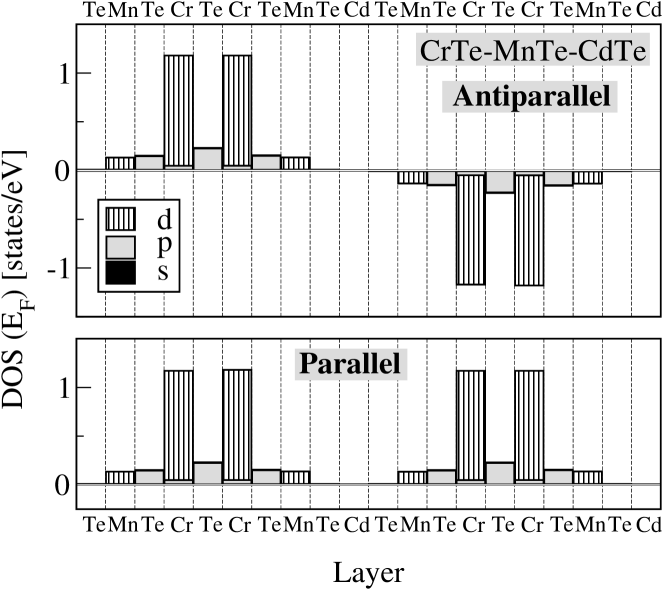
We verified these predictions by first-principles calculations. We used the full-potential linearized augmented plane-wave method as implemented in the FLEUR code, within the generalized gradient approximation of density-functional theory, using the CdTe lattice constant. In Table 1 we present the calculated geometry in more detail. A supercell was used in the calculation, consisting of two “leads”, each having two Cr and two Mn layers (and corresponding Te layers), separated by a CdTe layer for decoupling. Various possible magnetic configurations were examined. In the ground state (AP in Table 1), the leads are AP coupled, as expected. In addition, the Mn atoms are antiferromagnetically coupled to the Cr atoms. The nice feature is that, in the ground state, each lead is by itself half-metallic, so that the whole system is non-conducting. This is evident also from Fig. 2, where the layer-resolved density of states at is shown. Spin-down electrons are blocked in the first half of the junction, whereas spin-up electrons are blocked in the second part. By applying an external magnetic field the system switches to the P configuration with an energy cost of 15 meV (per CdTe slab). The P state is half-metallic throughout the junction and conducting by tunneling of spin-up electrons, as can be seen in Fig. 2 (bottom).
The switching energy from the AP to the P state can be tuned by introducing more CdTe layers. To show this, we compare the case without a CdTe layer (the interface is then of the form Mn-Te-Mn), where meV, to the case of Mn-CdTe-Mn ( meV), and then to the case of Mn-CdTeCdTe-Mn ( meV). Each additional CdTe layer lowers the energy difference by an order of magnitude. One or two more CdTe layers should decouple the layers sufficiently.
In summary, we have discussed the use of half-metallic ferromagnets in TMR and GMR junctions. We concluded that, while in GMR junctions the half-metallic property can be exploited fully, in TMR junctions the same property does not help if there are interface states present at within the half-metallic gap of the half-metal / insulator interface (as is typical for Heusler alloys). The reason is that the tunneling rate is slow compared to the spin-flip rate, whence minority-spin interface states are efficiently coupled to the metallic reservoir of the majority-spin states.
We have also proposed that such TMR elements can be made by using half-metallic zinc-blende pnictides and chalcogenides in contact with II-VI semiconductors, which show no interface states at . In this case we showed that, under certain conditions, an antiparallel magnetic coupling of the leads is possible, blocking the electric current completely. Such a device will show ideal magnetoresistance ratio and can serve as an ideal magnetic field sensor.
We are grateful to Prof. H. Akinaga, Prof. P. H. Dederichs, and Dr. G. Bihlmayer for fruitful discussions.
References
- (1) R.A. de Groot, F.M. Mueller, P.G. van Engen, and K.H.J. Buschow, Phys. Rev. Lett. 50, 2024 (1983).
- (2) M. Bowen, M. Bibes, A. Barthélémy, J.-P. Contour, A. Anane, Y. Lemaitre, and A. Fert, Appl. Phys. Lett. 82, 233 (2003).
- (3) Ph. Mavropoulos, K. Sato, R. Zeller, P. H. Dederichs, V. Popescu, and H. Ebert, Phys. Rev. B 69, 054424 (2004); Ph. Mavropoulos, I. Galanakis, V. Popescu and P.H. Dederichs, J. Phys.: Condens. Matter 16, S5759 (2004).
- (4) G.A. de Wijs and R.A. de Groot, Phys. Rev. B 64, 020402(R) (2001); I. Galanakis, M. Ležaić, G. Bihlmayer, and S. Blügel, arXiv:cond-mat/0409333 (2004); I. Galanakis, J. Phys.: Condens. Matter 16, 8007 (2004); A. Debernardi, M. Peresi, and A. Baldereschi, Comp. Mat. Sci. 33, 263 (2005); S. Picozzi, A. Continenza, and A.J. Freeman, J. Phys. Chem. Solids 64, 1697 (2003).
- (5) I. Galanakis, P. H. Dederichs, and N. Papanikolaou, Phys. Rev. B 66, 134428 (2002); I. Galanakis, P. H. Dederichs, and N. Papanikolaou, ibid 66, 174429 (2002); S. Picozzi, A. Continenza, and A.J. Freeman, ibid 69, 094423 (2004); S. Picozzi, A. Continenza, and A.J. Freeman, ibid 66, 094421 (2002).
- (6) For an indirect measurement of see, e.g., S. Kämmerer, A. Thomas, A. Hütten, and G. Reiss, Appl. Phys. Lett. 85, 79 (2004).
- (7) I. Galanakis, J. Phys.: Condens. Matt. 14, 6329 (2002); M. Ležaić, I. Galanakis, G. Bihlmayer, and S. Blügel, arXiv:cond-mat/0502597 (2005); S.J. Jenkins, Phys. Rev. B 70, 245401 (2004).
- (8) Ph. Mavropoulos, I. Galanakis, and P. H. Dederichs, J. Phys.: Condens. Matter 16, 4261 (2004); K. Nagao, M. Shirai, and Y. Miura, J. Appl. Phys. 95, 6518 (2004).
- (9) H. Akinaga, T. Manago, and M. Shirai, Jpn. J. Appl. Phys. 39, L1118 (2000); M. Mizuguchi, H. Akinaga, T. Manago, K. Ono, M. Oshima, and M. Shirai, J. Magn. Magn. Mater. 239, 269 (2002).
- (10) J. H. Zhao, F. Matsukura, K. Takamura, E. Abe, D. Chiba, and H. Ohno, Appl. Phys. Lett. 79, 2776 (2001).
- (11) K. Ono, J. Okabayashi, M. Mizuguchi, M. Oshima, A. Fujimori, and H. Akinaga, J. Appl. Phys. 91, 8088 (2002).
- (12) J. Okabayashi, M. Mizuguchi, K. Ono, M. Oshima, A. Fujimori, H. Kuramochi, and H. Akinaga, Phys. Rev. B 70, 233305 (2004).
- (13) J. H. Zhao, F. Matsukura, K. Takamura, D. Chiba, Y. Ohno, K. Ohtani, and H. Ohno, Mat. Sci. in Semicond. Processing 6, 507 (2003).
- (14) M. Mizuguchi, H. Akinaga, T. Manago, K. Ono, M. Oshima, M. Shirai, M. Yuri, H. J. Lin, H. H. Hsieh, and C. T. Chen, J. Appl. Phys. 91, 7917 (2002).
- (15) P. Bruno, Phys. Rev. B 52, 411 (1995).
- (16) M. Shirai, Physica E 10, 143 (2001); A. Sakuma, Journal of the Physical Society of Japan 71, 2534 (2002).
- (17) I. Galanakis and Ph. Mavropoulos, Phys. Rev. B 67, 104417 (2003); I. Galanakis, ibid 66, 012406 (2002); S. Sanvito and N. A. Hill, ibid 62, 15553 (2000); A. Continenza, S. Picozzi, W. T. Geng, and A.J. Freeman, ibid 64, 085204 (2001); W.-H. Xie, Y.-Q. Xu, B.-G. Liu , and D. G. Pettifor, Phys. Rev. Lett. 91, 037204 (2003).
- (18) S.-H. Wei and A. Zunger, Phys. Rev. B 35, 2340 (1987).