Ordered Nano-Crystal Arrays Spontaneously Form in Films Evaporated onto Nanopore Array Substrates
Abstract
We present SEM images of films thermally evaporated onto Anodic Aluminum Oxide substrates that are patterned with a hexagonal array of 34 and 80 nm diameter holes spaced by 100 nm. Over a range of film thicknesses, Pb and Sn films spontaneously self assemble into an array of nano-crystals in registry with the underlying hole lattice. The development of the arrays with thickness indicates that surface energies drive coalescing grains to move over the holes. Materials that wet the substrate or whose grains do not coalesce at these substrate temperatures do not form arrays. We discuss some potential applications.
Many approaches to create nanoscale structures in metals and semiconductors have been explored for the development of improved devices such as higher density magnetic memory Moser et al. (2002); Sun et al. (2000); Thurn-Albrecht et al. (2000) and the investigation of fundamental scientific problems, such as the Kondo effect Liang et al. (2002). One approach has been to grow films on substrates with nanometer scale strucutre Gao et al. (2001); Chik and Xu (2004) that serve as templates. For example, superconducting films deposited on carbon nanotubes form wires that are suitable for investigations of one dimensional superconductiviy Bezryadin et al. (2000). Also, Anodic Aluminum Oxide (AAO) substrates with hexagonal nanopore arrays have been employed to pattern superconducting Nb films with nano holes on the order of the superconducting coherence length for the study of vortex ordering Welp et al. (2002).
In the cases mentioned above, the deposited films assumed the structure of their substrates. That is, the metal films on carbon nanotubes are as one dimensional as the nanotubes Bezryadin et al. (2000) and the films on the hexagonal pore array develop a hexagonal hole pattern Welp et al. (2002). Here we show that the interaction between the films and the substrate can lead to film structure that differs dramatically from the substrate structure. Specifically, Pb and Sn films thermally evaporated onto AAO substrates spontaneously form a hexagonal array of nano-crystals that are in registry with the holes (i.e. the negative of the substrate). The detailed evolution of this film structure with thickness and comparisons with the growth of other metals on these substrates suggest that surface energies drive the nano-crystal array formation.
The AAO substrates employed here were fabricated using established procedures Chik and Xu (2004); Masuda and Fukuda (1995); Li et al. (1999). A Scanning Electron Microscopy image of one of them is shown in the inset in Fig. 1. The average diameters of the holes in the arrays employed were and 80 nm and the standard deviation of the hole diameters was about 5%. The depth of the holes greatly exceeded the interhole spacing, nm. Elemental films (Pb, Sn, Au, Pd, Ge) were thermally evaporated onto AAO substrates held at room temperature in a vacuum of approximately Torr. The quoted thicknesses correspond to the mass per unit area deposited, as measured by a quartz crystal microbalance, divided by the bulk density of the material. Each film shown in the figures was made in a single evaporation step.
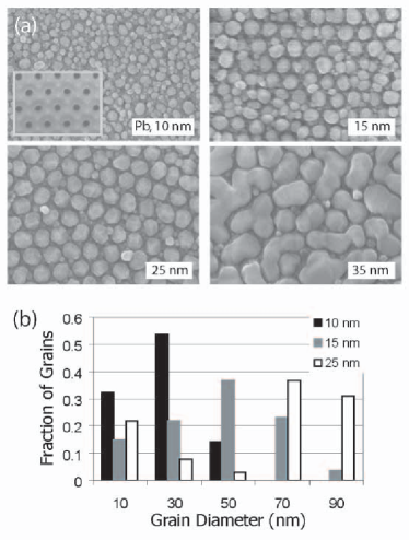
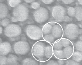
The spontaneous formation of nano-crystals is demonstrated in Figs. 1, 2, and 3. The SEM images in Fig. 1 depict Pb films of different thicknesses on the AAO substrates with 34 nm diameter holes. At the lowest thickness, nm, the grains are randomly distributed and their size distribution peaks at a diameter, , near 30 nm, with few grains with nm. Interestingly, at this stage the holes in the substrate are almost completely obscured by the grains. With increasing thickness to nm, larger grains appear. The grain size distribution develops a peak near nm and extends to include grains 70 nm in diameter and more. Simultaneously, the largest grains spontaneously assemble into a hexagonal array. At nm, the grain diameter distribution exhibits a peak at even higher diameters (centered on nm) and the hexagonal ordering is strongest. The spatial period of the grain array coincides closely with that of the underlying lattice of holes. This coincidence is brought out by the large area image in Fig. 2. Not only is the local ordering hexagonal, but the grain arrangements exhibit domains and defects similar to those in the nanopore arrangements. Finally, the magnified image in the inset of Fig. 2 reveals that the large grains are faceted indicating that they are single crystals.
Pb films deposited on AAO substrates with larger holes ( nm) with the same spacing ( nm) also spontaneously form an ordered array of grains. The details of their morphological evolution differs slightly (see Fig. 3) from that described above and in a manner that provides further insight into the grain array formation process. At the lowest thicknesses, the Pb grains do not obscure the holes, but rather, they ‘roughen’ the hole edges. With increasing film thickness, the grains grow and as they become comparable to the size of the necks between holes, gradually obscure the holes. Eventually, at nm the grains form an ordered array and assume a relatively narrow size distribution similar to the results on the substrate with 34 nm holes. The grain sizes (diameter of about 90 nm) and the film thickness ( nm) necessary for the array formation, however, are larger than on the 34 nm hole substrate. Finally, in thicker films, grains covering neighboring holes start to coalesce (not shown).
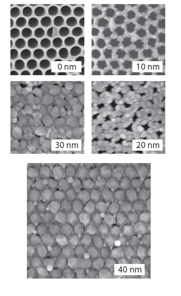
We have also observed spontaneous nano-crystal array formation in Sn films on 34 nm hole AAO substrates through a similar evolution as shown in Fig. 1 for Pb. Again, the Sn grains grow with film thickness and form over the holes at a thickness at which the grains become comparable to the hole size. On the other hand, grain arrays do not form for Au, Pd, and Ge films. As shown in Fig. 4, Au and Pd films reproduce the substrate geometry, but gradually fill in the holes as the film thickness increases. Unlike the Pb and Sn films, these films either have grains that do not change their size with film thickness (Au) or do not have grains at all (Ge, Pd).
There are two features exhibited during film growth that appear essential for the formation of the ordered array of nano-crystals:
-
1.
The materials must not wet the substrate so that grains can form
-
2.
The temperature of the substrate, , must be high enough that the mobility of the deposited atoms, crystalline defects, and grain boundaries is high enough to promote coalescence.
Pb and Sn films, for which the ratios of the substrate temperature to the elemental melting temperature, , are lowest, exhibit both of these features. Grains are clearly evident in their SEM images indicating non-wetting of the substrate. The wide distribution of grain diameters in the thinner films, the growth in the average grain diameter with coverage and more directly, the observation of grains caught in the process of combining (see nm film in Fig. 1) are consistent with grain growth through coalescence and accretion of deposited atoms. During deposition, grains grow, touch and coalesce. The randomness of the nucleation and coalescence processes gives rise to the distribution of grain
sizes. By contrast, while Au films do form grains and thus do not wet the substrate, their grain size distribution is comparatively uniform and the average grain size does not change with thickness. These characteristics indicate that grain coalescence does not occur in them. Pd and Ge films do not form grains that are large enough to be resolved in the SEM images and thus, appear to wet the substrate.
The fact that the Pb grains form in perfect registry with the holes indicates that the grains find it energetically most favorable to be off the substrate. A liquid drop model Ohring (1992) of the thin film growth appears to be a sufficient description of the free energies involved. The difference between the free energy of a grain on the substrate and a grain of the same size and shape over a hole is approximately
| (1) |
where is the energy of the interface formed by the substrate and the metal crystal facet in contact with it, is the surface energy of the metal crystal facet and is the substrate surface energy. The areas of the grain in contact with the surface and not in contact with the surface are and respectively. The total area of a grain is . For a grain over a hole to be in the lowest free energy state, , or .
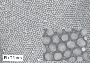
Close inspection of the Pb SEM images suggests that this free energy difference provides the force driving the grains to form over the holes. In the coalescence process, grains hanging over a hole find it energetically favorable to pull their partner toward the hole to minimize the surface in contact with the substrate. This type of process ‘roughens’ the edges of the holes on the 80 nm hole substrate at nm and leads to the near complete closing of the holes at nm. On the 34 nm hole substrate (see Fig. 5), it is possible to see clusters of grains centered on a point where a hole is likely to be. The regular arrangement of the larger grains around them makes it possible to ascertain the positions of the clusters relative to underlying holes. The grains in these clusters presumably are on the verge of coalescing and would have coalesced and left a large grain over the hole, had the film been made slightly thicker.
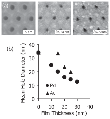
Within this simple picture it is possible to understand why the Pd, Ge and Au films do not form ordered arrays of grains. In the case of the Pd and Ge films, adatom diffusion rates are so low at room temperature that the film structure is consistent with the deposited atoms sticking where they land and wetting the substrate. Presumably the interactions between the substrate and these elements are very strong. Grain formation in the Au films suggests that there is some adatom motion. The grain size, however, depends very weakly on film thickness indicating that grain coalescence does not occur in Au films on room temperature substrates. Typically, is necessary for the thermally activated motion necessary for grain growth through coalescence Long and Valles (2005). For K, is 0.22 for Au.
It is important to note that other methods that produce nano-dots with AAO substrates differ qualitatively from the one presented in this paper. Masuda and coworkers separated the anodized portion of the substrate from the underlying aluminum and used it as an evaporation mask to produce arrays of metal dots Masuda et al. (2000). Gao and coworkers produced an ordered array of hemispherical Au dots by depositing Au on the underlying aluminum portion. This substrate had hemispherical depressions in its surface that the evaporated metal filled. It is likely that surface energies played a role in driving the Au into the depressions.
The mechanism that we have considered suggests that it should be possible to extend this technique to the formation of arrays of other metals or nanostructures of other geometries. For instance, we speculate that higher melting temperature non-wetting metals such as Au would also show grain ordering if the deposition is carried out at higher substrate temperatures. The spontaneous formation of these arrays through the interaction of the deposited films with the substrate structure suggests that it may be possible to engineer other nano-structures in thin films using suitably patterned substrates. For example, one could envisage the spontaneous formation of an array of parallel metal wires on a substrate with narrow parallel trenches.
Potentially, the fabrication of these grain arrays can be used as the first step in the creation of ordered superconducting junction arrays consisting of nanometer scale superconducting islands. An overlayer of semiconductor or metal deposited on the arrays could provide the necessary inter-island coupling. The lack of processing involved in their fabrication ensures that the interfaces in the junctions remain free of contaminants. Moreover, the small size of these islands and the spatial extent of their arrays are hard or impossible to produce using standard lithographic techniques. Thus, it seems plausible to create novel ordered arrays with a superconductor to insulator that can be compared to that of disordered granular filmsValles et al. (1994). Similarly, these arrays are suitable for investigations of a recently proposed superconductor to metal quantum phase transition Feigel’man et al. (2001); Spivak et al. (2001); Kouh and Valles (2003).
Pb and Sn films deposited on room temperature AAO substrates with a hexagonal array of holes spontaneously form an ordered array of nanometer scale crystals. The arrays first form at film thicknesses at which the grain sizes are comparable to the hole diameters. The grains appear to grow primarily through coalescence. Since the films do not wet the substrate at all, the coalescence events are biased by surface energies to drive the grains over the holes. Films composed of grains that do not coalesce (e.g. Au) or that wet the substrate, do not form ordered arrays of grains (e.g. Pd, Ge).
Acknowledgements: We are grateful for helpful discussions with Professors Ben Freund and Humphrey Maris. This work has been supported by the NSF through DMR-0203608 and an REU supplement, AFRL and ONR.
References
- Moser et al. (2002) A. Moser, K. Takano, D. T. Margulies, et al., J. Phys. D: Appl. Phys. 35, R157 (2002).
- Sun et al. (2000) S. H. Sun, C. B. Murray, D. Weller, et al., Science 287, 1989 (2000).
- Thurn-Albrecht et al. (2000) T. Thurn-Albrecht, J. Schotter, C. A. Kastle, et al., Science 290, 2126 (2000).
- Liang et al. (2002) W. J. Liang, M. P. Shores, M. Bockrath, et al., Nature 417, 725 (2002).
- Gao et al. (2001) T. Gao, J. C. Fan, G. W. Meng, et al., Thin Solid Films 401, 102 (2001).
- Chik and Xu (2004) H. Chik and J. M. Xu, Mater. Sci. Eng., R (2004).
- Bezryadin et al. (2000) A. Bezryadin, C. N. Lau, and M. Tinkham, Nature 404, 971 (2000).
- Welp et al. (2002) U. Welp, Z. L. Xiao, J. S. Jiang, et al., Phys. Rev. B 66, 212507 (2002).
- Masuda and Fukuda (1995) H. Masuda and K. Fukuda, Science 268, 1466 (1995).
- Li et al. (1999) J. Li, C. Papadopoulos, J. M. Xu, et al., Appl. Phys. Lett. 75, 367 (1999).
- Ohring (1992) M. Ohring, The Materials Science of Thin Films (Academic Press Inc, Boston, 1992).
- Long and Valles (2005) Z. Long and J. M. Valles, Jr., J. Low Temp. Phys. 139, 429 (2005).
- Masuda et al. (2000) H. Masuda, K. Yasui, and K. Nishio, Adv. Mater. 12, 1031 (2000).
- Valles et al. (1994) J. J. M. Valles, S. Y. Hsu, R. C. Dynes, et al., Physica B 197, 522 (1994).
- Feigel’man et al. (2001) M. V. Feigel’man, A. I. Larkin, and M. A. Skvortsov, Phys. Rev. Lett. 86, 1869 (2001).
- Spivak et al. (2001) B. Spivak, A. Zyuzin, and M. Hruska, Phys. Rev. B 64, 132502 (2001).
- Kouh and Valles (2003) T. Kouh and J. J. M. Valles, Phys. Rev. B 67, 140506 (2003).