Present address: ]Graduate School of Information Science and Technology, Hokkaido University, Sapporo, 060-0814, Japan Present address: ]Graduate School of Engineering, Tohoku University, Sendai, 980-8579, Japan
Experimental realization of a ballistic spin interferometer based on the Rashba effect using a nanolithographically defined square loop array
Abstract
The gate-controlled electron spin interference was observed in nanolithographically defined square loop (SL) arrays fabricated using In0.52Al0.48As/In0.53Ga0.47As/In0.52Al0.48As quantum wells. In this experiment, we demonstrate electron spin precession in quasi-one-dimensional channels that is caused by the Rashba effect. It turned out that the spin precession angle was gate-controllable by more than 0.75 for a sample with m, where is the side length of the SL. Large controllability of by the applied gate voltage as such is a necessary requirement for the realization of the spin FET device proposed by Datta and Das [Datta et. al., Appl. Phys. Lett. 56, 665 (1990)] as well as for the manipulation of spin qubits using the Rashba effect.
pacs:
71.70.Ej, 73.20.Fz, 73.23.Ad, 73.63.HsExploitation of spin degree of freedom for the conduction carriers provides a key strategy for finding new functional devices in semiconductor spintronics awschalombook02 ; datta90 ; koga02filter ; nitta99 ; bercioux04 ; kato05 . A promising approach for manipulating spins in semiconductor nanostructures is the utilization of spin-orbit (SO) interactions. In this regard, lifting of the spin degeneracy in the conduction (or valence) band due to the structural inversion asymmetry is especially called the “Rashba effect” rashba60 ; bychkov84 , the magnitude of which can be controlled by the applied gate voltages and/or specific design of the sample heterostructures nitta97 ; koga02wal .
Recently, we proposed a ballistic spin interferometer (SI) using a square loop (SL) geometry, where an electron spin rotates by an angle due to the Rashba effect as it travels along a side of the SL ballistically koga04 . In a simple SI model, an incident electron wave to the SI (see Fig. 1 in Ref. koga04, ) is split by a “hypothetical” beam splitter into two partial waves, where each of these partial waves follows the SL path in the clockwise (CW) and counter-clockwise (CCW) directions, respectively. Then, they interfere with each other when they come back to the incident point (at the beam splitter). As a consequence, the incident electron would either scatter back on the incident path (called “path1”) or emerge on the other path (called “path2”). The backscattering probability to path1 () for the case that the incident electron is spin unpolarized is given by koga04 ,
| (3) |
where is the quantum mechanical phase due to the vector potential responsible for the magnetic field piercing the SL (, being the side length of the SL) and is the spin precession angle when the electron propagates through each side of the SL due to the Rashba effect (, and being the Rashba SO coupling constant and the electron effective mass, respectively). A plot of as a function of is found in Ref. koga04, . We note that corresponds to the amplitude of the Al’tshuler-Aronov-Spivak(AAS)-type oscillation of electric conductance experimentally altshuler81 . Equation (3) predicts that the amplitude of the AAS oscillation should be modulated as a function of , which, in turn, can be controlled by the applied gate voltage through the variation of the values.
In this Letter, we present the first experimental demonstration of the SI using nanolithographically defined SL arrays in epitaxially grown (001) In0.52Al0.48As/In0.53Ga0.47As/In0.52Al0.48As quantum wells (QW). Details of the sample preparation are following: we use the same MOCVD-grown epi-wafers of In0.52Al0.48As/In0.53Ga0.47As/In0.52Al0.48As QWs as those we used for the weak antilocalization (WAL) study previously (samples1-4 in Ref. koga02wal, ). We first exploit the electron beam lithography (EBL) and electron cyclotron resonance (ECR) plasma etching techniques to define an array of SLs in the area of 150200 m2. We then use the photolithography and wet etching techniques to form a Hall bar mesa of the size of 125250 m2 over the SL array regions. In this way, the area of the final SL array region in the Hall bar mesa is 125200 m2 [see Fig. 1(b)]. These samples have a gate electrode (Au) covering the entire Hall bar, using a 100 nm thick SiO2 layer as a gate insulator, which makes it possible to control the sheet carrier density and the Rashba spin-orbit parameter by the applied gate voltage . We note that all the measurements were carried out at 0.3 K using a 3He cryostat, exploiting the conventional ac lock-in technique. When the electric sheet conductivities of these samples were measured [using the electrodes labeled by , , and in Fig. 1(b)] as a function of ( to the sample surface) for a given [denoted as ], the Hall voltages were also measured using the electrodes labeled by and . In this way, we were able to monitor and at the same time for each given . We then investigate the amplitude of the AAS oscillations at [denoted as ], as a function of (equivalently ), to test the prediction of the SI koga04 .
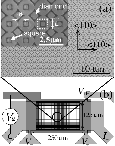
Examples of the scanning electron micrographs (SEM) of the SL pattern used in the present experiment are shown in Fig. 1(a). We note that electrons exist in the relatively lighter regions of the picture. The relatively darker lines and curves that define the “diamond” () and “square” () shapes in Fig. 1(a), are the dry-etched regions by the ECR plasma etching. We note that electrons exist in these diamond- and square-shaped islands. However, these islands do not contribute to the electric conductivity, since they are not electrically connected one another. We sketch a SL path for the spin interference by the dotted white square in the inset of Fig. 1(a), where electrons would be localized if the type of the spin interference is constructive. The width of the SL path is also defined in Fig. 1(a). We used m throughout the present experiment. We can see that these SLs are electrically connected with the neighboring SLs. As a result, they contribute to the electric conductivity of the whole Hall bar.
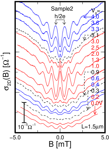

Shown in Fig. 2 is the gate voltage () dependence of for a SL array sample (m) that is fabricated using the sample2 epi-wafer in Ref. koga02wal, . Here, we clearly see the AAS oscillations, whose period () is given by . We also note that as the value of is increased from 0.0 V, the peak feature in at become dip across V [a dashed curve]. Then, the dip feature becomes peak for V [also indicated by another dashed curve]. Finally the peak feature again becomes dip for V. Thus the amplitudes of the AAS oscillations at oscillate as a function of as predicted in Eq. (3).
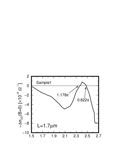
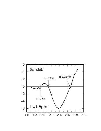
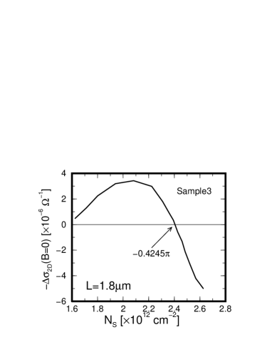
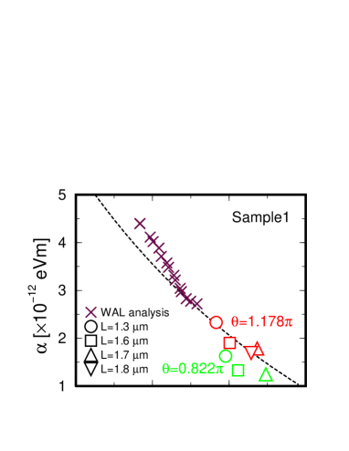
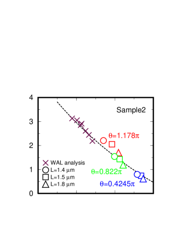
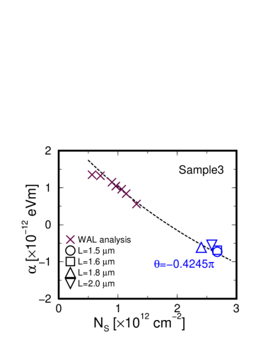
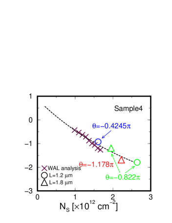
Plotted in Fig. 3 are the amplitudes of the experimental AAS oscillation at [denoted as ] as a function of for the SI devices fabricated using the sample 14 epi-wafers ( and 1.5 m for samples 1 and 2, respectively, and m for samples 3 and 4), where we employed the Fast Fourier Transform (FFT) and inverse FFT techniques to extract only the oscillatory part of whose period corresponds to the magnetic flux half quanta . We indeed see that oscillates with , where we observe several nodes. Using the vs. relations that are obtained from the WAL analysis of an unpatterned QW sample and the model calculation using appropriate boundary conditions koga02wal , values for sample 2 at these node positions [denoted as below], for example, are identified as (from left to right) 1.178, 0.822 and 0.4245 (see Fig. 2 in Ref. koga04, ). We thus demonstrated that the spin precession angle is gate-controllable by more than 0.75 for a length of 1.5m. The values for the other SI devices using the other epi-wafers are also identified in Fig. 3. We can, then, calculate the values at these node positions using the relation .
In Fig. 4, we plot the values obtained in this way (denoted as ) for various SL array samples made of the sample1-4 epi-wafers as a function of . Also plotted in Fig. 4 are (1) the values obtained from the WAL analysis of the unpatterned (bare) Hall bars (denoted as ) and (2) those obtained from the model calculations (denoted as ) using the appropriate boundary conditions and assuming the presence of the background impurities koga02wal . We note that the unpatterned Hall bars for are prepared on the same wafer pieces as those used for the SL array samples. We also note that in Ref. koga02wal, we obtained values without assuming the background impurities and found quantitatively good agreement with values. In the present work, we included the effect of the background impurities (mostly they are present in the In0.52Al0.48As buffer layer) in the model calculation of to better fit the experimental and values. It turned out that the values of the background impurity densities obtained from these fittings are reasonably small (typically 11016 cm-3). The details of this analysis are discussed elsewhere sekine05 .
In summary, we have demonstrated experimentally the electron spin interference phenomena based on the Rashba effect, which are predicted previously koga04 . For this demonstration, we prepared nanolithographically defined square loop array structures in In0.52Al0.48As/In0.53Ga0.47As/In0.52Al0.48As quantum wells using the electron beam lithography and ECR dry etching techniques and measured the low-field magnetoresistances of these samples ( sample surface) at low temperatures (0.3 K). We observed the Al’tshuler-Aronov-Spivak (AAS) oscillations, whose magnitudes at oscillated as a function of the gate voltage as the result of the spin interference. We also deduced the values (Rashba spin-orbit coupling constant) from the analysis of the spin interferometry experiments. We obtained quantitative agreements among (1) the values obtained from the spin interferometry experiments, (2) those obtained from the weak antilocalization analysis, and (3) those obtained from the model calculations.
References
- (1) D. Awschalom, N. Samarth, and D. Loss, Semiconductor Spintronics and Quantum Computation (Springer Verlag, 2002).
- (2) S. Datta and B. Das, Appl. Phys. Lett. 56, 665 (1990).
- (3) T. Koga, J. Nitta, H. Takayanagi, and S. Datta, Phys. Rev. Lett. 88, 126601 (2002).
- (4) J. Nitta, F. E. Meijer, and H. Takayanagi, Appl. Phys. Lett. 75, 695 (1999).
- (5) D. Bercioux, M. Governale, V. Cataudella, and V. M. Ramaglia, Phys. Rev. Lett. 93, 056802 (2004).
- (6) Y. K. Kato, R. C. Myers, A. C. Gossard, and D. D. Awschalom, Appl. Phys. Lett. 86, 162107 (2005).
- (7) E. I. Rashba, Sov. Phys. Solid State 2, 1109 (1960), [Fiz. Tverd. Tela (Leningrad) 2, 1224 (1960)].
- (8) Y. A. Bychkov and E. I. Rashba, J. Phys. C 17, 6039 (1984).
- (9) J. Nitta, T. Akazaki, H. Takayanagi, and T. Enoki, Phys. Rev. Lett. 78, 1335 (1997).
- (10) T. Koga, J. Nitta, T. Akazaki, and H. Takayanagi, Phys. Rev. Lett. 89, 046801 (2002).
- (11) T. Koga, J. Nitta, and M. van Veenhuizen, Phys. Rev. B 70, 161302(R) (2004).
- (12) B. L. Al’tshuler, A. G. Aronov, and B. Z. Spivak, JETP Lett. 33, 94 (1981).
- (13) Y. Sekine, T. Koga, and J. Nitta, (2005), unpublished.