[
Spin accumulation in degenerate semiconductors near modified Schottky contact with ferromagnets
Abstract
We study spin transport in forward and reverse biased junctions between a ferromagnetic metal and a degenerate semiconductor with a doped layer near the interface at relatively low temperatures. We show that spin polarization of electrons in the semiconductor, , near the interface increases both with the forward and reverse current and reaches saturation at certain relatively large current while the spin injection coefficient, , increases with reverse current and decreases with the forward current. We analyze the condition for efficient spin polarization of electrons in degenerate semiconductor near interface with ferromagnet. We compare the accumulation of spin polarized electrons in degenerate semiconductors at low temperatures with that in nondegenerate semiconductors at relatively high, room temperatures.
pacs:
72.25.Hg, 72.25.Mk]
I Introduction
The idea of novel solid state electronic devices using a electron spin has given rise to the new field of spintronics [1, 2]. Among practically important spintronic effects are the giant magnetoresistance in magnetic multilayers and the tunnel ferromagnet-insulator-ferromagnet (FM-I-FM) structures [3, 4, 5]. Of particular interest is injection of spin-polarized electrons into semiconductors because of large spin relaxation time [7] and a prospect of using this phenomena for the next generation of high-speed low-power electronic devices [6, 8, 9] and quantum computing [1]. Relatively efficient spin injection into nonmagnetic semiconductors (S) has been demonstrated at low temperatures in ferromagnet-semiconductor heterostructures both with metallic ferromagnets [10, 11, 12] and magnetic semiconductors [13] as the spin sources. Theoretical aspects of the spin injection have been studied in Refs. [14, 15, 16, 17, 18, 19, 20, 21, 22, 23, 24, 25, 26].
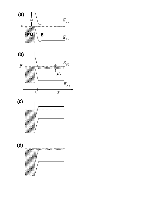
There are several fundamentally different types of FM-S junctions with the energy band diagrams shown in Fig. 1. The band diagrams depend on electron affinity of a semiconductor, , and a work function of a ferromagnet, , electron density in a semiconductor, , and a density of surface states at the FM-S interface [27]. Usually, a depleted layer and a high Schottky potential barrier form in S near metal-semiconductor junction, Fig. 1a,b, at and even when due to the presence of surface states on the FM-S interface [27]. In some systems with a layer with accumulated electrons can form in S near the FM-S interface, Figs. 1c,d. Such a rare situation is probably realized in Fe-InAs junctions studied in Ref. [12]. The barrier height in the usual situation (Figs. 1a,b) is equal to eV for GaAs and Si in contacts with practically all metals, including Fe, Ni, and Co [27, 11]. The barrier width, i.e. the Schottky depleted layer width, is large, nm, for doping donor concentration cm-3. The injection of spin polarized electrons from FM into S corresponds to a reverse current in the Schottky contact, when positive voltage is applied to S region. The current in reverse-biased FM-S Schottky contacts is saturated and usually negligible due to such large barrier thickness and height, and [27]. Therefore, a thin heavily doped S layer between FM metal and S should used to increase the reverse current determining the spin-injection [19, 25]. This layer drastically reduces the thickness of the barrier, and increases its tunneling transparency [27, 25]. Thus, an efficient spin injection has been observed in FM-S junctions with a thin layer [11].
In forward-biased FM-S Schottky contacts without the thin layer, current can reach a large value only at a bias voltage close to , where is the elementary charge [27]. Realization of the spin accumulation in S due to such thermionic emission currents is problematic. Indeed, electrons in FM with energy well above the Fermi level are weakly spin polarized.
The energy band structure of FM-S junctions, their spin-selective and nonlinear properties have not been actually considered in majority of theoretical works on spin injection [14, 15, 16, 17, 18, 19, 20, 21, 22, 23, 24]. Authors of these prior works have developed a linear theory of spin injection describing the spin-selective properties of FM-S junctions by various, often contradictory, boundary conditions at the FM-S interface. For example, Aronov and Pikus assumed that a spin injection coefficient (spin polarization of current in FM-S junctions) at the FM-S interface is a constant, equal to that in the FM metal, and studied spin accumulation in semiconductors considering spin diffusion and drift in applied electric field [14]. The authors of Refs. [15, 16, 17, 18, 19] assumed a continuity of both the currents and the electrochemical potentials for both spins and found that a spin polarization of injected electrons depends on a ratio of conductivities of a FM and S (the so-called “conductivity mismatch” problem). At the same time, the authors of Refs. [20, 21, 22, 23, 24] have asserted that the spin injection becomes appreciable when the electrochemical potentials have a substantial discontinuity at the interface (produced by e.g. a tunnel barrier [21]). However, they described this effect by the unknown constants, spin-selective interface conductances , which cannot be found within those theories. In fact, we have shown before that the parameters are not constant and can strongly depend on the applied bias voltage [9, 25].
In our earlier works [9, 25, 26] we have studied the nonlinear spin injection in nondegenerate semiconductors near modified FM-S Schottky contacts with doped layer, Fig.1a, at room temperature and showed that the assumptions made in Refs. [15, 16, 17, 18, 19] are not valid at least in that case. Here we derive the boundary conditions and study nonlinear spin injection in degenerate semiconductors near reverse- and forward-biased FM-S Schottky contacts with an ultrathin heavily doped semiconductor layer (doped layer) between FM and S, Fig. 1b. In degenerate semiconductors, unlike in nondegenerate semiconductors studied in Refs. [25, 26], the spin injection can occur at any (low) temperatures. We consider below the case when the temperature , where is the Fermi energy of equilibrium electrons in S, where is the bottom of the conduction band in equilibrium, Fig. 1, and is the temperature in units of .
II Spin tunneling through thin doped barrier at FM-S interface
We assume that the donor concentration, , and thicknesses, , of the doped layer satisfy the conditions and where is a typical tunneling length ( nm for cm-3). The energy band diagram of such a FM-S junction includes a potential spike of the height and the thickness shown in Fig. 1b. We assume the elastic coherent tunneling through this layer, so that the energy , spin and the component of the wave vector parallel to the interface, , are conserved. In this case the tunneling current density of electrons with spin near the FM-S junction containing the doped layer (Fig. 1) can be written as [28, 5, 25, 26]
| (1) | |||||
| (2) |
where is the transmission probability, the Fermi function, the component of velocity of electrons with the wave vector and spin in the ferromagnet, the integration includes a summation with respect to a band index. Importantly, one needs to account for a strong spin accumulation in the semiconductor. Therefore, we use the nonequilibrium Fermi levels, and for electrons with spin in the FM metal and the semiconductor, respectively, near the interface, . In particular, the local electron density with spin in the degenerate semiconductor at the FM-S junction at low temperatures is given by
| (3) | |||||
| (4) |
where the number of effective minima of the semiconductor conduction band; and are the bottom of conduction band in S at equilibrium and at the bias voltage , is the equilibrium Fermi energy of the electrons in the semiconductor bulk, with the Fermi level in FM metal bulk, is the quasi Fermi level in S near the interface (point Fig. 1), and are the concentration and effective mass of electrons in S. We note that and current in forward-biased FM-S junctions , i.e. flows in direction from FM to S when (usual convention [27]), and and in reverse biased junctions. The current (2) should generally be evaluated numerically for a complex band structure [29]. The analytical expressions for can be obtained in an effective mass approximation, where is the velocity of electrons in the FM with spin . This applies to “fast” free-like d-electrons in elemental ferromagnets [30, 5]. Approximating the barrier by a triangular shape, we find
| (5) | |||||
| (6) |
where , , is the component of the velocity of electrons in S, , the “tunneling” velocity, (for comparison, for a rectangular barrier and ), for and zero otherwise. The preexponential factor in Eq. (6) takes into account a mismatch between effective mass, and , and velocities, and , of electrons in the FM and the S. Obviously, only the states with are available for transport.
We obtain the following expression for the current at the temperature with the use of Eqs. (2) and (6), noting that the electron velocity in the semiconductor is singular near
| (8) | |||||
where the second integral corresponds to electrons tunneling from the metal into semiconductor that can only take place when As a rule, and are smooth functions over in range of interest to us in comparison with a singular . At not very large bias voltages of interest, all factors but can be taken outside of integration. We obtain, therefore, from (4) and (8) the expression
| (11) | |||||
which with use Eq. (4) can be finally written as
| (13) | |||||
where
| (14) |
| (15) |
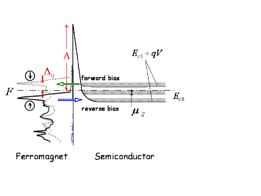
Here ; ; is the velocity of electrons in the degenerate semiconductor, the velocity of electrons in the FM (taken at and for reverse and forward bias voltages, respectively, see below), , and is the splitting of the quasi Fermi level for nonequilibrium electrons with spin in FM metal. We notice that only spin factor determines the dependence of current on materials parameters of a ferromagnet. The need for a different choice of for forward and reverse bias voltage is evident from Fig. 2. At forward bias the electrons tunnel from the semiconductor into the states in the ferromagnetic metal at , so there At reverse bias voltage the electrons tunnel to the semiconductor in the interval of energies In this case the effective tunnel barrier height is smallest for electrons with energies , so . Moreover, at reverse bias a spatial charge starts to build in semiconductor and a wide barrier forms at energies Therefore, only electrons in narrow energy range can tunnel, and the reverse current practically saturates at
Finally, we can present the currents of electrons with spin at the interface in the following useful form:
| (17) | |||||
where
| (18) |
and
| (19) |
As we see below the value of determines maximum spin polarization.
At small bias voltage when and are much smaller than and by linearizing Eq. (13) we obtain
| (20) | |||||
| (21) |
where and are the electrochemical potentials at FM-S interface in the semiconductor and ferromagnet, respectively, is the spin-selective interface linear conductance. It is worth noting that if we were to use the assumption of Refs. [15, 16, 17, 18, 19] about a continuity of the electrochemical potentials at FM-S junction, , we must have concluded that no current flows through the junction, . We note that the boundary condition similar to Eq. (21) was used in a linear theory of spin injection in Refs. [20, 21, 22, 22, 24], where were introduced as some phenomenological constants. Here, we have found the explicit expressions for the spin conductances for the FM-S junction under consideration. Obviously, , as well as and are not universal and depend on all specific parameters of the junctions, Fig. 1 (cf. Ref. [25]). Moreover, the conclusions drawn from the linear approximation strongly differ from the results of a full nonlinear analysis provided below (see also Ref. [25]).
Importantly, we can neglect the quasi Fermi splitting in FM metal compared to that in the semiconductor because the density of electrons in the FM metal is several orders of magnitude larger that in real semiconductors. It is easy to prove that for the currents of interest to us (see Appendix B), therefore we can simplify the expression (17) for tunneling currents of spin-polarized electrons as
| (23) | |||||
III Injected and extracted spin polarization in degenerate semiconductor
The assumption of elastic coherent tunneling means a continuity of the currents of spin-polarized electrons through the FM-S junction. In this case the FM-S junction can be characterized by the spin injection coefficient according to the definition:
| (24) |
where are the currents of electrons with near the FM-S interface, Fig. 1. Notice that is the spin polarization of a current in the FM-S junction, therefore we used symbol instead of in our earlier papers [9, 25, 26].
The following derivation of bi-spin diffusion applies to both semiconductor and ferromagnet based on an assumption of quasineutrality (see Appendix B). The current is given by
| (25) |
where , and are the conductivity, the diffusion constant, the mobility and the density of electrons with spin , respectively, the electric field in S or FM. We assume quasineutrality, and later prove that it holds very well indeed (see Appendix A) and a continuity of the total current, , so that one has
| (26) |
and for the electric field
| (27) |
where is the total conductivity of S or FM. Substituting (27) into (25), we find
| (28) |
where is the bi-spin diffusion constant for the semiconductor or ferromagnet.
The bi-spin diffusion that appears in the case of degenerate semiconductors is different in comparison with nondegenerate semiconductor where and do not depend on spin orientation (see Refs. [14, 18, 25]). In degenerate semiconductors we need to account for the density dependence of the diffusion constant. We will assume that the relaxation time of electron momentum weakly depends on a quasi- Fermi level (i.e. on electron density). Therefore, the mobility of electrons in nonmagnetic semiconductors in question weakly depends on the electron density. In this case we can put , and at low temperature, where and are the diffusion coefficient in a non-polarized semiconductor and the total conductivity of the semiconductor, respectively. The account for a density-dependent diffusion coefficient gives the following expression for the bi-spin diffusion coefficient:
| (29) | |||||
| (30) |
where
| (31) |
and we have introduced the spin polarization of electrons
| (32) |
When the polarization is small, (as is always the case at distances from the interface), the bi-spin diffusion coefficient has only quadratic corrections to the usual diffusion coefficient, and is quite close to the diffusion coefficient in a nondegenerate semiconductor
In nonmagnetic semiconductors the electron density is determined by the continuity equation [14, 18]
| (33) |
where , is the total density of equilibrium electrons , is spin-coherence lifetime of electrons in S. The expression for current (28) now gives
| (34) |
We can rewrite this as an equation for the polarization distribution using and as
| (35) |
where is the dimensionless coordinate and
| (36) |
are the typical spin-diffusion length and the characteristic current density. It is very convenient to rewrite the spin currents (28) through as
| (37) |
The spin currents at the interface should be equal to the tunneling spin currents through FM-S junction given by Eq. (23). With the use , this gives the main boundary condition at the interface
| (38) | |||||
| (39) |
where
| (40) |
the spin polarization next to the interface. It is easy to see that the equation (35) becomes linear away from the interface where . Therefore, it has an asymptotic behavior [14, 18, 25]
| (41) | |||||
| (42) |
where the coefficient would have been equal for ( case) like in nondegenerate semiconductor [25]. The stationary polarization distribution is found from equation (35) solved with the boundary conditions (39) and (41).
Interestingly, the effect of nonlinearity of the diffusion coefficient in degenerate semiconductors, given by the function in Eq.(31), appears to be very small. This is confirmed by comparing the solution of (35) with the case of constant diffusion coefficient, , but we first give simple arguments why this is so. Nonlinearity could have only been important in the equation (35) when the polarization is close to unity, , so that At the same, relatively large can only be achieved at a large current and a large polarization in ferromagnet, (i.e. for a half-metallic FM [5]), but even in this case remains considerably smaller than see Fig. 3 and discussion below. As a result, the polarization dependence of the diffusion changes the polarization profile very little, see Fig. 3 where we compare the exact polarization profile with that for
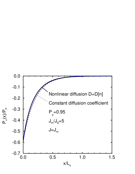
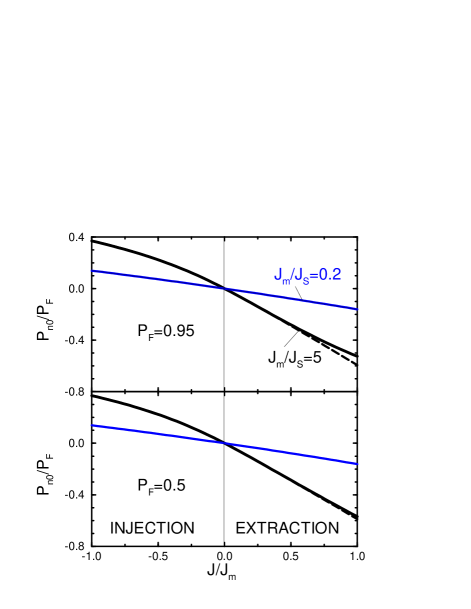
We study the current dependence of the polarization in Fig. 4. It illustrates two important points: (i) the effect of the polarization of injected carriers in a semiconductor and (ii) the effect of having different maximal currents through the structure in comparison with the characteristic current density . We see that the difference between the polarization-dependent and independent diffusion coefficients is minute at all parameters. A small difference is only present for the spin extraction near maximal current for where the non-linearity in the diffusion coefficient slightly reduces the extracted polarization. In the opposite case of relatively small maximal current, the difference in polarizations is not discernible at all. The case of is of most interest to us, since there the absolute value of the accumulated polarization is maximal. The overall behavior of the injected/extracted polarization with the current is similar to the one we found for non-degenerate semiconductors [9, 26].
Since we have determined that the density dependence of the diffusion coefficient in a semiconductor has little effect, the solution of the kinetic equation (35) reduces to (41), (42), where the prefactor . The boundary condition (39) then simplifies to
| (43) |
This is similar to the case of nondegenerate semiconductor, the difference being the term in square brackets, which is specific for the degenerate semiconductor.
General analytical solution for polarization is readily found by noticing that the right hand side of Eq. (43) is very close to a linear function of at all values of parameters. Therefore, a general solution for the polarization in degenerate semiconductor can be written very accurately as
| (44) | |||||
| (45) |
As expected, vanishes with current, when , and increases in absolute value when the current approaches maximum. It follows from Eq. (45) that the polarization can reach an absolute maximum only when , where the maximal injected polarization is and the maximal extracted polarization is
The solution for (45) together with the expression for current (23) allows one to obtain the I-V curve. The closed expression for the I-V curve can be obtained in the case of small bias voltage where
| (46) |
where according to (18) and depend on . The equation (46) is a transcendental one, but at when we have and it becomes and an expression for the current that starts as an Ohmic law
| (47) |
and then deviates from it at larger bias.
The behavior of injection coefficient is very different compared to the polarization. Using the relation (37) for (neglecting the polarization dependence of the diffusion coefficient) and Eqs. (45),(36), (42) we find a relation between the injection coefficient (polarization of current) and the polarization of density
| (48) | |||||
| (49) |
The injection coefficient does not vanish with current, but tends to a finite value
| (50) |
In order to maximize the polarization , according to Eq. (45), one needs to use the modified Schottky contact with (transparent for tunneling electrons), where the injection coefficient would be very small, In this case, at large forward current so the spin injection coefficient practically vanishes in spin extraction regime (in other words, the polarization of current vanishes). Very differently, under reverse bias voltage so that the polarization of the injected current is large. Note that here we still assume that the densities of carriers in the FM metal and the degenerate semiconductor are vastly different, so that there is a clear “conductivity mismatch” and yet the spin injection proceeds very efficiently. On the other hand, if we were to make the contact opaque, where the polarization of electrons, according to Eq. (45), would become minute, since the current through the structure becomes very small compared to the characteristic current that polarizes electrons, . But at the same time, the injection coefficient becomes large, This is the same behavior as observed in FM-I-FM tunnel junctions [5]: relatively thick tunnel barriers facilitate strong polarization of current but the accumulated spin polarization remains very small since the current density is insufficient.
The described behavior of the polarization and the injection coefficient is very important for proper understanding of the behavior of spintronic structures. In particular, we have demonstrated once again an ill-conceived nature of the “conductivity mismatch” problem [17]. The condition of the maximum spin accumulation in semiconductor, , in accordance with Eqs. (18), (40) and (36) can be written down as
| (51) |
This condition can be rewritten with the use of Eq. (46) at as
| (52) |
where is the tunneling contact resistance. We emphasize that Eq. (52) is opposite to the condition of maximum of current spin polarization found in Ref. [21] for small currents. At , i.e. when , as we noted above, a degree of spin accumulation in the semiconductor is very small, , but exactly this is the characteristic that determines chief spin effects [1, 6, 8, 25]. Note that the condition (52) does not depend on the electron concentration, therefore it coincides with that for nondegenerate semiconductors (see [25]).
IV Discussion
We obtained an analytical solution for spin injection/extraction for degenerate semiconductor in addition to numerical results for nonlinear spin diffusion. The nonlinear dependence of the bi-spin diffusion coefficient in semiconductor on accumulated polarization appears to be small. We emphasize that the value of (19) determining maximum spin polarization of the FM-S junction depends on bias voltage , because the spin factor given by Eq. (15) is determined by . Since usually the spin factor . In a metal, as a rule, therefore where is the density of states of the d-electrons with spin and energy in the ferromagnet. Thus, assuming we find from Eq. (19) that . The polarization of d-electrons in elemental ferromagnets Ni, Co, and Fe is reduced by the current of unpolarized s-electrons , where is a factor (roughly the ratio of the number of s-bands to the number of d-bands crossing the Fermi level). Together with the contribution of s-electrons the polarization parameter is approximately
| (53) |
We note that such a relation for can be obtained from a standard “golden-rule” type approximation for tunneling current that is supposed to be proportional to the density of states (cf. Refs. [27, 31, 33]). The density of states for minority d-electrons in Fe, Co, and Ni has a large peak at ( eV), much larger than for the majority electrons and for electrons [34, 35], Fig. 2. Therefore, the spin polarization and spin injection coefficient can potentially achieve a large value of in the forward-biased FM-S at a bias voltage (Fig. 2). In reverse biased junctions the situation is different in that most effective tunneling is by electrons in FM with energies close to the Fermi level, where the polarization of carriers is positive, [35] and a good fraction of it may be injected into a semiconductor. In this case the excess of majority spins may be created in semiconductor for both reverse (injection) and forward (extraction) bias voltages. This implies a complex dependence of accumulated spin polarization on a bias voltage.
V Conclusion
Let us compare spin injection in the modified Schottky FM-S junctions with degenerate semiconductor at low temperatures with nondegenerate semiconductors at large (room) temperature. In both cases the process of spin injection/extraction strongly depends on current density and is generally nonlinear. The condition for most efficient spin accumulation is similar in both cases, that sets constraints on materials parameters, see Eq. (51). We have studied this case for both reverse [25] and forward bias voltages [26].
We have shown that the spin injection in reverse-biased FM-S junctions differs from that in the forward-biased junctions. In the reverse-biased junctions spin polarization of injected electrons, , and spin injection coefficient, , increase with current up to a maximum where is the polarization of ferromagnet, Fig. 4. In forward-biased FM-S junctions the polarization approaches at large currents in a shrinking region with the width In this case the spin injection coefficient is small, already at and decreases at large current, Analogous results are obtained in Refs. [25, 26] for the FM-S junctions with nondegenerate semiconductors, with the only difference that at forward current when the minority electrons are extracted into the energy region with a peak in the density of states. The I-V characteristics for Schottky contacts with degenerate and non-degenerate semiconductors are also quite different.
It is worth mentioning a different dependence of effective polarization of ferromagnet (19) on bias voltage in both cases. In a nondegenerate semiconductor corresponds to the electron energy for a degenerate semiconductor it is . The value of for the nondegenerate semiconductor can reach its maximum at a reverse bias voltage ( eV) while for degenerate semiconductor can have the same large value at a forward voltage , Fig. 2. In a nondegenerate semiconductor, has the same sign practically independently of the bias while in the degenerate semiconductor may change sign with bias voltage and, at least potentially, can become close to unity at the forward bias , but not at a reverse bias. Under reverse bias voltage, the electrons are injected into the degenerate semiconductor from states in the ferromagnet with energies where their polarization is The predicted strong dependence of accumulated polarization on bias voltage can be exploited in order to reveal possible effect of peaks in the density of states. Indeed, if the filling of the conduction band of the degenerate semiconductor is relatively small, eV, as is usually the case, then by changing the forward bias one could “scan” the density of states in FM with a “resolution” Fig. 2. One may see an increase in current and a maximum in an extracted polarization at Interestingly, one may expect a sign change of the polarization in FM-S modified Schottky contact with a degenerate semiconductor S.
A Electroneutrality
A deviation from the quasineutrality is determined by the continuity equations (33) with the Poisson equation (in CGS units)
| (A1) |
where is the dielectric constant of the material and is the deviation of electron density from equilibrium one. We show here that and, therefore, can be neglected. To this end, we substitute the expression for the electric field, Eq.(27) into (A1) and obtain the following estimate
| (A2) | |||||
| (A3) |
where is the screening length in the degenerate semiconductor (Thomas-Fermi length). We have used the Einstein relation where is the density of states at the Fermi level. Finally, the required estimate for deviations from electroneutrality becomes
| (A4) |
For example, in Si at doping cm-3 the screening length is Å and with m one obtains , a very small deviation from electroneutrality indeed that can be safely neglected (cf. this with attempts to account for deviations from electroneutrality in Ref. [2]).
B Quasi-Fermi level splitting in ferromagnet and semiconductor
Let us prove that we indeed can neglect the splitting of the quasi-Fermi level in FM metal, , compared to the splitting of the quasi-Fermi level in semiconductor for the FM-S junction under consideration. Since we can neglect the electric field in FM metal, the distribution of spin polarized electrons is determined by their diffusion: in FM, i.e. in the region corresponding to , Fig. 1. Thus, according to (28) the currents of spin polarized electrons in FM near FM-S interface are
| (B1) |
We find from (B1) and (24) that which gives
| (B2) |
where we have introduced
| (B3) |
the spin polarization of a current in the FM bulk. Thus, if we were to make the same assumption as Aronov and Pikus in Ref. [14] that , we would have obtained and, consequently, . In other words, there would be no splitting at all of the Fermi levels in a ferromagnet in Aronov-Pikus approximation. In reality, there is a splitting of the quasi-Fermi levels in FM, but it is usually small compared to the splitting in the semiconductor (see estimates below). This allows us to considerably simplify the description of the spin injection/extraction.
According to Eqs. (B2) and (49),
| (B4) |
where . We have shown that the polarization of current and it may be therefore,
The ratio of and is approximately equal to
| (B5) |
where , and are the Fermi energies for electrons in FM and S, respectively. Since the electron density in FM metals, cm-3, is several orders of magnitude larger than in S (typically, cm-3), the value . Thus, one can see from (B5) that indeed . We showed above (see also Ref. [26]) that is small at very large forward currents, therefore, can be on the order of . However, such current corresponds to the bias voltages of Schottky junctions . Due to the condition we can indeed neglect in Eq. (17), so the approximation used to derive the Eqs. (17) and (39) is justified.
We emphasize that the conclusion is valid for FM-S Schottky junctions. Possible exception can only be the FM-S junctions with an accumulation layer, Fig. 1d. In such FM-S junctions the electron density in S near the FM-S interface can be very large. In such rare case both and can be on the order of unity, perhaps allowing for and even . However, this case requires a separate study where one has also to take into account spin selective properties of such a FM-S junctions and a steep spatial variation of electron density in S near the FM-S interface, Fig. 1d.
REFERENCES
- [1] Semiconductor Spintronics and Quantum Computation, edited by D.D. Awschalom, D. Loss, and N. Samarth (Springer, Berlin, 2002); S. A. Wolf, D. D. Awschalom, R. A. Buhrman, J. M. Daughton, S. von Molnar, M. L. Roukes, A. Y. Chtchelkanova, D. M. Treger, Science 294, 1488 (2001); D. P. DiVincenzo, Science 270, 255 (1995); G. A. Prinz, Phys. Today 48, 58 (1995); N. A. Gershenfeld and I. L. Chuang, Science 275, 350 (1997); B. E. Kane, Nature 393, 133 (1998); H. Ohno, D. Chiba, F. Matsukura, T. Omiya, E. Abe, T. Dietl, Y. Ohno, K. Ohtani, Nature 408, 944 (2000); D. Loss and D. P. DiVincenzo, Phys. Rev. A 57, 120 (1998).
- [2] I. Zutic, J. Fabian, and C. Das Sarma, Rev. Mod. Phys. 76, 323 (2004).
- [3] M.N. Baibich, J. M. Broto, A. Fert, F. Nguyen Van Dau, F. Petroff, P. Etienne, G. Creuzet, A. Friederich, and J. Chazelas, Phys. Rev. Lett. 61, 2472 (1988); A. E. Berkowitz, J. R. Mitchell, M. J. Carey, A. P. Young, S. Zhang, F. E. Spada, F. T. Parker, A. Hutten, and G. Thomas, ibid. 68, 3745 (1992); Ultrathin Magnetic Structures, edited by B. Heinrich and J. A. C. Bland (Springer, Berlin, 1994); J. S. Moodera, L.R. Kinder, T. M. Wong, and R. Meservey, Phys. Rev. Lett. 74, 3273 (1995); T. Miyazaki and N. Tezuka, J. Magn. Magn. Mater. 139, L231 (1995).
- [4] J.C. Slonczewski, Phys. Rev. B 39, 6995 (1989).
- [5] A. M. Bratkovsky, Phys. Rev. B 56, 2344 (1997).
- [6] S. Datta and B. Das, Appl. Phys. Lett. 56, 665 (1990); S. Gardelis, C. G. Smith, C. H. W. Barnes, E. H. Linfield, and D. A. Ritchie, Phys. Rev. B 60, 7764 (1999).
- [7] A. G. Aronov, G.E. Pikus, and A.N. Titkov, Sov. Phys. JETP 57, 680 (1983); J. M. Kikkawa, I.P. Smorchkova, N. Samarth, D. D. Awschalom, Science 277, 1284 (1997); J. M. Kikkawa and D. D. Awschalom, Phys. Rev. Lett. 80, 4313 (1998); D. Hägele, M. Oestreich, W. W. Rühle, N. Nestle, and K. Eberl, Appl. Phys. Lett. 73, 1580 (1998); M. Oestreich, J. Hübner, D. Hägele, P. J. Klar, W. Heimbrodt, W. W. Rühle, D. E. Ashenford, and B. Lunn, Appl. Phys. Lett. 74, 1251 (1999); J. M. Kikkawa and D. D. Awschalom, Nature 397, 139 (1999); I. Malajovich, J. J. Berry, N. Samarth, D. D. Awschalom, Nature 411, 770 (2001); I. Malajovich, J. M. Kikkawa, and D. D. Awschalom, J. J. Berry and N. Samarth, Phys. Rev. Lett. 84, 1015 (2000); R. M. Stroud, A. T. Hanbicki, Y. D. Park, G. Kioseoglou, A. G. Petukhov, B. T. Jonker, G. Itskos, and A. Petrou, Phys. Rev. Lett. 89, 166602 (2002).
- [8] R.Sato and K. Mizushima, Appl. Phys. Lett. 79, 1157 (2001); X.Jiang, R. Wang, S. van Dijken, R. Shelby, R. Macfarlane, G. S. Solomon, J. Harris, and S.S.P. Parkin, Phys. Rev. Lett. 90, 256603 (2003).
- [9] A. M. Bratkovsky and V.V. Osipov, Phys. Rev. Lett. 92, 098302 (2004); V.V. Osipov and A. M. Bratkovsky, Appl. Phys. Lett. 84, 2118 (2004).
- [10] P. R. Hammar, B. R. Bennett, M. J. Yang, and M. Johnson, Phys. Rev. Lett. 83, 203 (1999); M. Tanaka and Y. Higo, Phys. Rev. Lett. 87, 026602 (2001); H.J. Zhu, M. Ramsteiner, H. Kostial, M. Wassermeier, H.-P. Schönherr, and K. H. Ploog , ibid. 87, 016601 (2001); W. Y. Lee, S. Gardelis, B.-C. Choi, Y. B. Xu, C. G. Smith, C. H. W. Barnes, D. A. Ritchie, E. H. Linfield, and J. A. C. Bland, J. Appl. Phys. 85, 6682 (1999); T. Manago and H. Akinaga, Appl. Phys. Lett. 81, 694 (2002); A. F. Motsnyi, J. De Boeck, J. Das, W. Van Roy, G. Borghs, E. Goovaerts, and V. I. Safarov, ibid. 81, 265 (2002); C. Adelmann, X. Lou, J. Strand, C. J. Palmstrøm, and P. A. Crowell, Phys. Rev. B 71, 121301(R) (2005).
- [11] A. T. Hanbicki, B. T. Jonker, G. Itskos, G. Kioseoglou, and A. Petrou, Appl. Phys. Lett. 80, 1240 (2002); A. T. Hanbicki, O. M. J. van’t Erve, R. Magno, G. Kioseoglou, C. H. Li, and B. T. Jonker, ibid. 82, 4092 (2003).
- [12] H. Ohno, K. Yoh, K. Sueoka, K. Mukasa, A. Kawaharazuka, and M. E. Ramsteiner, Jpn. J. Appl. Phys. 42, L1 (2003).
- [13] V.V. Osipov, N.A.Viglin, and A.A. Samokhvalov, Phys. Lett. A 247, 353 (1998); Y. Ohno, D. K. Young, B. Beschoten, F. Matsukura, H. Ohno, and D. D. Awschalom, Nature 402, 790 (1999); R. Fiederling, M. Keim, G. Reuscher, W. Ossau, G. Schmidt, A. Waag, and L. W. Molenkamp, ibid. 402, 787 (1999).
- [14] A. G. Aronov and G. E. Pikus, Fiz. Tekh. Poluprovodn. 10, 1177 (1976) [Sov. Phys. Semicond. 10, 698 (1976].
- [15] M. Johnson and R.H. Silsbee, Phys. Rev. B 35, 4959 (1987); M. Johnson and J. Byers, ibid. 67, 125112 (2003).
- [16] P. C. van Son, H. van Kempen, and P. Wyder, Phys. Rev. Lett. 58, 2271 (1987); G. Schmidt, G. Richter, P. Grabs, C. Gould, D. Ferrand, and L. W. Molenkamp, ibid. 87, 227203 (2001).
- [17] G. Schmidt, D. Ferrand, L. W. Molenkamp, A. T. Filip and B. J. van Wees, Phys. Rev. B 62, R4790 (2000).
- [18] Z. G. Yu and M. E. Flatte, Phys. Rev. B 66, 201202(R) (2002).
- [19] J. D. Albrecht and D.L. Smith, Phys. Rev. B 66, 113303 (2002).
- [20] S.Hershfield and H.L.Zhao, Phys. Rev. B 56, 3296 (1997).
- [21] E. I. Rashba, Phys. Rev. B 62, R16267 (2000).
- [22] A. Fert and H. Jaffres, Phys. Rev. B 64, 184420 (2001).
- [23] C.-M. Hu and T. Matsuyama, Phys. Rev. Lett. 87, 066803 (2001).
- [24] Z.G. Yu and M.E. Flatte, Phys. Rev.B66, 235302(R) (2002).
- [25] V.V. Osipov and A.M. Bratkovsky, Phys. Rev. B 70, 205312 (2004).
- [26] A.M. Bratkovsky and V.V. Osipov, J. Appl. Phys. 96, 4525 (2004).
- [27] S. M. Sze, Physics of Semiconductor Devices (Wiley, New York, 1981); R. T. Tung, Phys. Rev. B 45, 13509 (1992).
- [28] C. B. Duke, Tunneling in Solids (Academic, New York, 1969).
- [29] S. Sanvito, C.J. Lambert, J.H. Jefferson, and A.M. Bratkovsky, Phys. Rev. B 59, 11936 (1999); O. Wunnicke, Ph. Mavropoulos, R. Zeller, P. H. Dederichs, and D. Grundler, Phys. Rev. B 65, 241306(R) (2002).
- [30] M.B. Stearns, J. Magn. Magn. Mater. 5, 167 (1977).
- [31] J. G. Simmons, J. Appl. Phys. 34, 1793 (1963); J. G. Simmons, J. Phys. D 4, 613 (1971); R. Stratton, Tunneling Phenomena in Solids, edited by E. Burstein and S. Lundqvist (Plenum, New York, 1969); R. T. Tung, Phys. Rev. B 45, 13509 (1992).
- [32] R. Gomer, Field Emission and Field Ionization (Harvard University Press, Cambridge, 1961); A. McConville, Emission Standards Handbook (Oxford University Press, NY, 1997).
- [33] L. Esaki, Phys. Rev. 109, 603 (1958); M. Julliere, Phys. Lett. 54A, 225 (1975).
- [34] V. L. Moruzzi, J. F. Janak, and A. R. Williams, Calculated Electronic Properties of Metals (Pergamon Press, New York, 1978); S. Chikazumi, Physics of Ferromagnetism (Oxford, New York, 1999).
- [35] I. I. Mazin, Phys. Rev. Lett. 83, 1427 (1999).