The origin of flux-flow resistance oscillations in
Bi2Sr2CaCu2O8+y:
Fiske steps in a single junction?
Abstract
We propose an alternative explanation to the oscillations of the flux-flow resistance found in several previously published experiments with Bi2Sr2CaCu2O8+y stacks. It has been argued by the previous authors that the period of the oscillations corresponding to the field needed to add one vortex per two intrinsic Josephson junctions is associated with a moving triangular lattice of vortices (out-of-phase mode), while the period corresponding to one vortex per one junction is due to the square lattice (in-phase mode). In contrast, we show that both type of oscillations may occur in a single-layer Josephson junction and thus the above interpretation is inconsistent.
pacs:
74.50.+r,74.40.+k,74.78.NaRecently, a lot of attention has been focused on the possible use of single crystals of Bi2Sr2CaCu2O8+y as generators of electromagnetic radiation in the THz range. Promising experiments in that direction were reported by Hirata et al. Hirata-PRL-2002 and shortly thereafter by Kakeya et al. Kakeya-2002-2004 and Hatano et al. Hatano-ASC-2004 . These experiments all showed oscillations in the flux-flow voltage and flux-flow resistance when a large magnetic field (of order several Tesla) was applied parallel to the plane in the presence of a small bias current in the –direction (of order a few percent of the critical current). The observed flux-flow voltage oscillations typically showed two different oscillation periods. At the lowest magnetic fields the period was corresponding to one extra flux quantum per two layers in the stack. Here is the magnetic flux quantum, and are the thickness and the length of the junction, respectively. At higher magnetic fields there was a transition to a period , i.e. corresponding to an extra flux quantum in every layer.
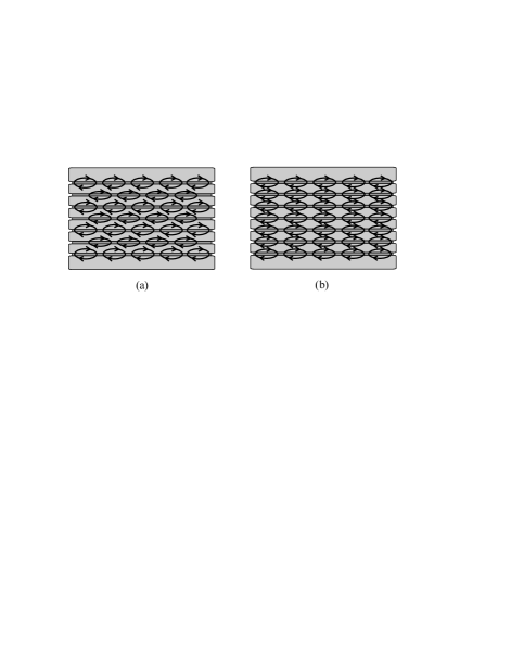
These exiting experiments were interpreted both analytically Koshelev-PRB-2002 and numerically Machida-PRL-2003 ; Tachiki-2004 ; Peders-Madsen-IEEE-2005 by several authors. One of the important questions to be answered was whether the flux lattice correspond to a triangular lattice (anti-phase ordering with possible cancellation of the sum voltage at the junction end) or a square lattice (in-phase ordering leading to a large sum voltage at the junction end). Figure 1 shows schematically a Bi2Sr2CaCu2O8+y stack with flux ordering in a triangular lattice and square lattice. Obviously, the latter case is highly preferable for applications to THz generation of electromagnetic waves; however simple intuition would suggest triangular ordering since fluxons of same polarity naturally repel each other. An intuitive interpretation of the experimentally observed oscillations in the flux-flow voltage would suggest that an oscillation period corresponds to triangular ordering while a period corresponds to a square lattice. Numerical simulations Machida-PRL-2003 ; Tachiki-2004 ; Peders-Madsen-IEEE-2005 have shown that both triangular and square lattices are possible, but their relation to regions of oscillations and regions of oscillations is not simple and details are still a matter of debate.
In this paper, we present fairly standard numerical simulations corresponding to the simplest case of a single-layer Josephson junction. Even for this case, where there is no triangular nor square lattice ordering (as our stack consists of only one junction), we find that both the and periods appear much the same way as in experiments and numerical simulations for Bi2Sr2CaCu2O8+y stacks with many layers and flux lattice ordering. After presenting the numerical simulations we provide a qualitative explanation in terms of the well-known Fiske modes Fiske-1964 .
The system under investigation is described by coupled sine-Gordon equations of the form SBP-1993 :
| (1) |
with
| (2) |
Here is the dissipation parameter (, , and are the normal resistance, the critical current and the capacitance per unit length, respectively), is the current normalized to the critical current of the individual junctions. The normalized coupling term among the junctions in the stack reads , where , is the thickness of one superconducting layer, and is the London penetration depth SBP-1993 . Time is normalized to the inverse of the Josephson plasma frequency and spatial coordinate is normalized with respect to the Josephson length . The magnetic field gives rise to boundary conditions of the form SBP-1993
| (3) |
Index stands here for the junction number in the stack and is the normalized length of the system.

Figure 2 shows the result of a simulation of the current-voltage characteristics for only one junction in the stack, i.e. . It shows the flux-flow branch of the junction with normalized length and damping constant placed in magnetic field . The characteristics is calculated by rising the bias current from zero to and then decreasing it back to zero. The voltage is given in normalized units chosen such that the voltage spacing between neighboring Fiske steps
| (4) |
is equal to unity (here is the Swihart velocity and is the physical length of the junction). The current-voltage characteristics displays fine structure due to the Fiske steps, which gather around the flux-flow voltage, also known as Eck peak Eck-peak . The hysteresis in this voltage region is due to the coexistence of several Fiske resonances at a given current . Some parts of these Fiske resonances are located inside the hysteresis and are not displayed on the plot.
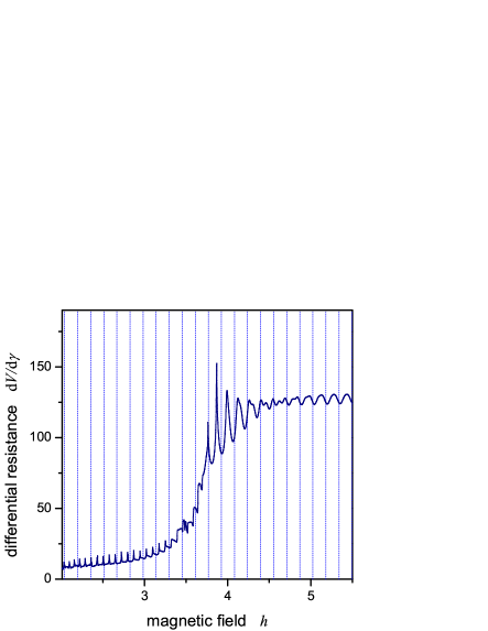
Using the above junction parameters, we calculated the dependence of the flux-flow resistance on magnetic field. Figure 3 presents the differential flux-flow resistance versus magnetic field at the fixed bias current . It clearly shows flux-flow resistance oscillations. In order to relate the period of oscillations with the number of vortices in the junction we show a grid in magnetic field with a period , which approximately corresponds to adding one vortex in the junction. This can be seen from the simple fact that at the critical field the normalized spacing between vortices penetrated into the junction is equal to , and their number rises proportionally to . In Fig. 3 we see that most oscillations have a characteristic period in corresponding to adding a half flux quantum into the junction, with a tendency of doubling the period at higher fields.
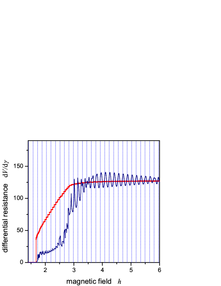
As another illustration, in Fig. 4 we show both static resistance and differential resistance versus magnetic field for the same junction but at a lower bias current . The oscillations of (thin curve) have two characteristic periods, which are found at different ranges of magnetic field . The oscillation period at low fields corresponds to about or less than half flux quantum, while at higher fields we find very clear oscillations which account for one flux quantum into the junction. The crossover from one regime to another occurs at magnetic field . Below this field the differential resistance at is lower as it is determined by the Eck peak (see also Fig. 2) composed of individual Fiske steps. At the Eck peak shifts to higher currents and the differential resistance levels at the resistive slope determined by the loss parameter of the junction. The static junction resistance (upper curve in Fig. 4) also changes in this range but its oscillations are much less pronounced and can only be clearly seen on the magnified scale.
We suggest the following explanation for the two oscillation periods of the flux-flow resistance in a single-barrier Josephson junction. At high enough magnetic field the resistance at a low bias current follows oscillations of the critical current of the junction and thus have a characteristic period of one flux quantum. At the same time, the resistance measured at a higher current (or lower field but the same bias current) follows the oscillations due to the Fiske steps, which envelope is associated with the Eck peak (sometimes called as flux-flow or velocity matching step). The matter is that – for a single junction – the Fiske steps induce a variation of the resistance with characteristic period corresponding to half flux quantum.
Fiske modes in a Josephson junction Fiske-1964 are linear cavity type excitations with resonance angular frequencies given by
| (5) |
in normalized units. The corresponding to wave vectors are
| (6) |
In experiments these Fiske modes are visible as current singularities in the current-voltage curve with a voltage spacing given by Eq. (4). The amplitude of the Fiske steps oscillate with the magnetic field in a typical Bessel function like pattern such that the even numbered steps have maxima together with maxima in the critical current, while maxima in the odd numbered steps correspond to minima in the critical current. Refs. Kulik ; Matteo-1998 give an approximate analytical form for the current-voltage curve for a single Josephson junction with Fiske steps. The current-voltage characteristics is approximately written as Matteo-1998 :
| (7) |
This approximation neglects high-order nonlinearities in the junction and is originally expected Kulik to describe well the case of short junction, i.e. . However, the comparison with long junction data made by Cirillo et al. Matteo-1998 shows that Eq. (7) can approximately account for the shape and for the maximum current modulation of the Fiske singularities in long () junctions when the field penetration overcomes Meissner shielding, i.e. at .
The first term in Eq. (7) represents the Ohmic part of the current-voltage characteristics, while the second term gives an infinite series of equidistant resonances. The height of the resonances is modulated by a slowly varying amplitude factor and a fast Fraunhofer amplitude factor Matteo-1998 . The Fraunhofer factor emphasizes the resonance closest to and drops off fast: If is an even multiple of , the odd numbered Fiske steps are enhanced and if is an odd multiple of , the even numbered Fiske steps survive.
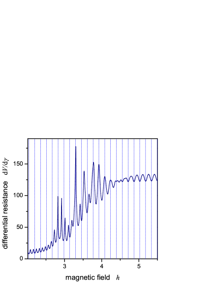
Equation (7) gives the current-voltage curve containing Fiske steps with the magnetic field as a parameter. If we instead assume a fixed bias current and vary the magnetic field, Eq. (7) expresses the voltage oscillations in an implicit form. In order to compare this analytical form with our simulations, we solved Eq. (7) for at a given numerically. The obtained the dependence of the flux-flow resistance at constant bias current versus magnetic field is presented in Fig. 5. The qualitative agreement between Figs. 3 and 4 obtained by full numerical simulation of the perturbed sine-Gordon equation and Fig. 5 emerging from the analytical formula (7) is strikingly good. Figure 5 clearly displays two characteristic periods of oscillations, namely half flux quantum oscillations at low fields and one flux quantum oscillations which become very explicit at high fields. The intermediate field range shows a complicated beating between two periods.
Thus, odd and even numbered Fiske resonances in the last term in Eq. (7) produce the ”magic” half-flux-quantum oscillations corresponding to the magnetic field period even in a single Josephson junction. Although we investigated here Fiske steps with , we note that Fiske steps are also present in stacks with Kim-Hatano:Plasma-2004 . Thus we are lead to suggest that also for the flux-flow voltage oscillations have their origin in the Fiske mode excitations.
We conclude that for Bi2Sr2CaCu2O8+y stacks the flux-flow voltage oscillations with two different periods in a magnetic field have their origin in the Fiske mode excitations. Thus the flux lattice ordering in either triangular or square lattice is not directly related to the two periods of the oscillations. We speculate that Fiske modes also existing in stacks indirectly play a role for the flux lattice formation.
We would like to acknowledge discussions with T. Hatano, S. Kim, A. E. Koshelev, S. Madsen, M. R. Samuelsen, H. B. Wang, and T. Yamashita.
References
- (1) S. Ooi, T. Mochiku, and K. Hirata, Phys. Rev. Lett. 89, 247002 (2002)
- (2) I. Kakeya, M. Iwase, T. Yamamoto, and K. Kadowaki, cond-mat/0503498 (2005); I. Kakeya et al. Physica C 378,406 (2002)
- (3) T. Hatano et al., IEEE Trans Appl. Superconduc., to be published
- (4) A.E. Koshelev, Phys. Rev B 66, 224514 (2002)
- (5) M. Machida, Phys. Rev. Lett. 90, 037001 (2003)
- (6) M. Tachiki, M. Iizuka, K. Minami, S. Tejima, and H. Nakamura, cond-mat/0407052 (2004)
- (7) N.F. Pedersen and S. Madsen, IEEE Trans Appl. Superconduc., to be published
- (8) M. D. Fiske, Rev. Mod. Phys. 36, 221 (1964)
- (9) S. Sakai, P. Bodin, and N.F. Pedersen, J. Appl. Phys. 73, 2411 (1993)
- (10) R. E. Eck, D. J. Scalapino and B. N. Taylor, Phys. Rev. Lett. 13, 15 (1964).
- (11) I. O. Kulik, Pis’ma Zh. Eksp. Teor. Fiz. 2, 134 (1965) [Sov. Phys. JETP Lett. 2, 84 (1965)]; I. O. Kulik, Zh. Tekhn. Fiz. 37 157 (1967) [Sov. Tech. Phys. 12, 111 (1967)]
- (12) M. Cirillo, N. Grønbech-Jensen, M. R. Samuelsen, M. Salerno, and G. V. Rinati, Phys. Rev. B 58, 12377 (1998)
- (13) S. Kim, S. Urayama, H. B. Wang, T. Hatano, M. Nagao, S. Kawakami, Y. Takano, and T. Yamashita. Poster Presentation in the conference ’Plasma-2004’ Tsukuba, Japan, November 2004