Coherent transport in homojunction between excitonic insulator and semimetal
Abstract
From the solution of a two-band model, we predict that the thermal and electrical transport across the junction of a semimetal and an excitonic insulator will exhibit high resistance behavior and low entropy production at low temperatures, distinct from a junction of a semimetal and a normal semiconductor. This phenomenon, ascribed to the dissipationless exciton flow which dominates over the charge transport, is based on the much longer length scale of the change of the effective interface potential for electron scattering due to the coherence of the condensate than in the normal state.
pacs:
71.35.Lk, 72.10.Fk, 73.40.Ns, 73.50.LwProposals that exciton condensation transforms a semimetal (SM) into an excitonic insulator (EI) date back more than four decades keldysh ; review ; Snoke . Experiments on indirect gap semiconductors exp and on coupled quantum wells butov have shown unusual properties which were inferred as indications of the exciton condensation. Earlier, the difficulties in distinguishing between the EI and the ordinary dielectric were pointed out Keldyshmaligno . Here we show that, if an EI exists, the larger coherence length scale of the exciton condensation allows the existence of a homojunction between an SM state and an EI state whereas the smaller length scale of the structural interface between a semimetal and a normal semiconductor gives it the nature of a heterojunction. Across the homogeneous SM/EI junction, the current is composed of two competing terms associated, respectively, with neutral excitons and with charge carriers. At small electrical bias and low temperature, exciton flow dominates over the free charges, increasing substantially the electrical and thermal interface resistance. The rate of entropy production is low due to the coherent and dissipationless character of the exciton flow, analogous to the case of a clean metal/superconductor (NS) junction.
Consider a model of two overlapping bands which form a semimetal as in the left panel of Fig. 1(a). A semiconductor (SC) may be formed either by a one-electron hybridization potential to a normal insulating state (NSC) or by a strong electron interaction between the two bands into an excitonic insulator. A normal semiconductor may, for example, be formed by changing an element in a compound for the semimetal and an excitonic insulator may be formed from the semimetal by strain or suitable alloying of the SM compound with a third element. Since the hybridization potential and the exciton condensation order parameter, , contribute additively to the small band gaps formed between the two overlapping bands as in the right panel of Fig. 1(a), the two resulting states cannot be distinguished by spectroscopy. We propose as an experimental means of identifying the EI state the transport properties across a junction with a sharp interface made of a semimetal and a small gap semiconductor, which is either normal or an EI. The key difference is in the length scale of the variation of the effective interface potential which reflects or transmits the electron. In the SM/EI junction, a component of the effective potential is the position dependent electron-hole paring potential, , which decreases from the bulk value in the EI region to zero in the SM region [see Fig. 2(a)]. The length scale of the change is the coherence length in EI, much longer than the lattice constant. The finite order in the SM region is due to the proximity effect of the exciton condensate in EI. Since this system works best if the lattices of the two components are as similar as possible, we classify the junction as homogeneous (termed homojunction by convention). On the other hand, in the SM/NSC junction, the one-electron interface potential due to the change in hybridization has an abrupt variation on a length scale of the order of a few atomic layers, thus considered in our context as a heterogeneous junction Schottky .
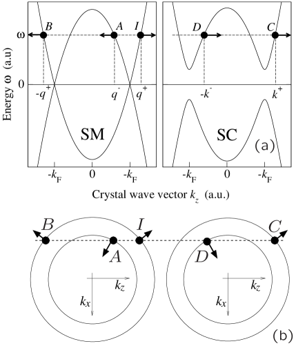
An important consequence of the interface potential is that carriers coming from the bulk SM with energies slightly outside the SC gap have, say for the incident electron at , two reflection channels, and , and two transmission channels at and (see Fig. 1). If the energy lies within the gap, only the two reflection channels are possible. While the interface by breaking the lattice translational symmetry can in principle connect different parts of the Brillouin zone SN , to express the results of our detailed model study of the interface scattering it is important to consider the regions of the wave vector space near the gaps in the bulk SC as two valleys for the states with the same component of the wave vector parallel to the interface. In the SM/EI homojunction, the slowly varying electron-hole pairing potential causes the dominant scattering to be intravalley, i.e., from to and . In the SM/NSC heterojunction, the rapid spatial variation of the interface potential causes strong intervalley reflection, i.e., from to , and strong intravalley transmission, i.e., from to . We have modeled the common physical features of the heterojunction, including the abrupt band edge discontinuity, the short-ranged interface potential, and the impurities at the interface (see Appendix). We shall now focus on the intravalley reflection arising out of the band mixing from the EI.
For simplicity of exposition, we take the effective masses of the two bands to be isotropic and equal to (Fig. 1). The electron quasi-particle excitation across the interface satisfies the mean-field equations
| (1a) | |||||
| (1b) | |||||
where the junction has been divided into small neighborhoods at positions , each being a homogeneous system with the Fermi wave vector and with the energy measured from the chemical potential, which is in the middle of the EI gap because of the conduction-valence band symmetry.
The conduction and valence band components of the quasi-particle wave function are defined Andreev , respectively, by and , where [] is the annihilation operator of an electron in the conduction (valence) band at position and time , and is the excited state, labeled by the index , obtained by adding one electron to the exact ground state, . The self-consistent order parameter or electron-hole pairing potential is a smooth function of the distance normal to the inferface, , tending respectively to the asymptotic values zero when , inside the bulk region of SM, and to the constant when , inside the bulk EI [Fig. 2(a)]. We consider the elastic scattering at equilibrium, matching wave functions of the incident (), transmitted ( and channels) and reflected ( and ) states at the boundary (Fig. 1), following Refs. Andreev ; BTK . We also calculate the particle density current, , where is the semiclassical group velocity and is the probability density.
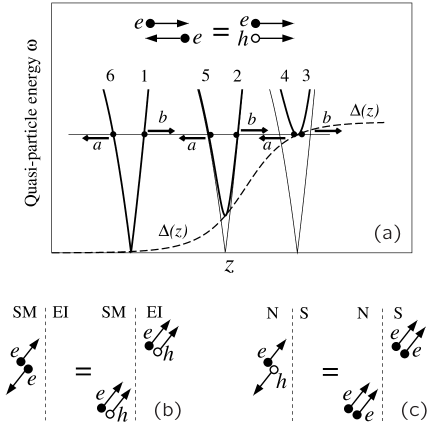
There are three qualitatively important results. First, all three cartesian components of the velocity of the reflected electron change sign [Fig. 2(b)]. This is not due to interface roughness since we take it to be completely flat. The exciton condensation causes the dominance of the intravalley reflection (from to and ) but examination of the scattering states on the Fermi surfaces in Fig. 1(b) shows that the state is an electron on the valence band Fermi surface with complete reversal of the velocity vector which may be regarded as a valence hole moving in the opposite direction. This is reminescent of the Andreev case Andreev when an incident electron is reflected as a hole from the NS boundary with the velocity reversed [Fig. 2(c)].
Second, the exciton condensate on the EI side induces exciton order on the SM side (the proximity effect). The off-diagonal contribution to the electronic density would be zero in an isolated SM but by the proximity with the condensate acquires the value
| (2) | |||||
where , and is the density of states. Inside the gap () each quasiparticle contributes to the sum (2) with a term . The only coordinate dependence enters this expression via the phase factor, , which represents the relative phase shift of conduction- and valence-band components of the wavefunction. If , then these components keep constant relative phase all the way to , where no pairing interactions exist. Therefore, the reflected electron has exactly the same velocity as the incident particle, and will thus retrace exactly the same path all the way to . At finite energy, the dependent oscillations provide destructive interference on the pair coherence. Hence, the paths of incident and reflected electrons part ways away from the interface. Analogous considerations apply to the incident electron and to the Andreev-reflected hole in a sub-gap scattering event at the NS interface Zagoskin .
Third, the ratio of incident electrons which are transmitted through the interface depends on the coherence factors of the condensate and is strongly suppressed close to the gap (see Appendix). The dependence of on and is formally identical to that for a bogoliubon across a NS interface, provided that the exciton binding energy is replaced with the BCS gap:
| (3) |
Below the gap the electron is totally “Andreev” reflected and the transmission is zero.
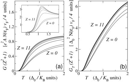
From the results for transmission and reflection probabilities, we derive in the linear response regime the values of the electrical and thermal interface conductances, and , respectively us ; usunpublished . The Seebeck coefficient is zero due to the symmetry artifact of the model Ziman2 . Then, except for an additive phonon contribution to the thermal conductance, the interface thermoelectric properties are completely determined by and . The curves in Fig. 3 show that and have an activation threshold at low temperature, , proportional to the gap . If , has exactly the same functional dependence on and in the SM/EI as in the NS junction. Remarkably, the rate of entropy production Ziman2 , , where and are the temperature and voltage drops at the interface and the cross-sectional area, is the same very low value in both cases. In the NS junction the term proportional to , unrelated to the superfluid component, comes from bogoliubons which, when they cross the NS interface, experience the same resistance as electrons do across the SM/EI boundary.
To shed light on the dissipationless motion of electrons in the linear transport regime, we place a -function potential barrier at , , simulating the effect of including a thin insulating layer BTK . Coherence between two sides of the interface is diminished as the dimensionless barrier strength, , increases from zero (clean junction) to finite values (tunneling regime). Figure 3 displays and for increasing values of . Since the transmission coefficient decreases uniformly in the absence of any electron-hole pairing (see Appendix), , we rescale conductances dividing them by . Naively, we would expect that the insertion of an insulating layer would reduce the conductances. On the contrary, the effect is just the opposite: as increases, and increase, eventually reaching saturation in the tunneling regime. This shows that the exciton order induced in the SM side by EI makes the junction less conductive for charge and heat transport. The plot of the differential conductance vs. at low [inset of Fig. 3(a)] allows clear monitoring of the transition from the transparent to the opaque limit, where transport is recovered. The effect is maximum for and as , when the diff. conductance becomes proportional to .
These features which distinguish the exciton insulator from the normal insulating state may be explained by two alternate physical pictures. The conventional view is that electrons below the energy gap cannot contribute to transport as they are back scattered by the gap barrier, , formed by proximity effect of the EI. The less conventional view is to make use of the analogy with the NS junction. Instead of counting the electrons in the valence band as negatively charged carriers of the current, we may start with the state with the valence band filled to the top as carrying zero current even under an electrical or thermal current and regard each unoccupied state in the valence band as a positively charged carrier — a hole — moving in the direction opposite to the electron. Then the reflected electrons are replaced by incoming holes towards the barrier. Therefore, the incident conduction electron and the valence hole may be viewed as a correlated pair moving towards the interface [Fig. 2(b)]. The novelty is that a constant electron-hole current moves from the SM to the EI below the gap, where electric transport is blocked. As the electron-hole pair approaches the interface from the SM side, the exciton current is converted into the condensate supercurrent: the global effect is that in the steady state an exciton current exists flowing constantly and reversibly all the way from the SM to the EI without any form of dissipation.
The above scenario follows from the continuity equation for the electron-hole current. The probability density for finding either a conduction-band electron or a valence-band hole at a particular time and place is . Thus, the associated continuity equation is
| (4) |
One component of the electron-hole current, , is the density current of the electron-hole pair, similar to the standard particle carrier with an important difference in sign. The other component, , depends explicitly on the built-in coherence of the electron-hole condensate , and may be described as the exciton supercurrent of the EI state.
Going back to our picture of smoothly varying in space (Fig. 2), if , each electron wave function, solution of Eq. (1), carries zero total electric current , which is the sum of the equal and opposite incident and reflected fluxes, and finite and constant electron-hole current , with a unit vector. When , far from the interface on the SM side, the supercurrent contribution is zero. As increases and gradually rises, both and conserve their constant value, independent of , since quasi-particle states are stationary. However, their analysis in terms of incident and reflected quasi-particles is qualitatively different. From the electron point of view, we see in Fig. 2(a) that the incoming conduction band particle approaching the EI boundary sees its group velocity progressively reduced, up to the classical turning point where it changes direction and branch of the spectrum: there is no net electric current. From the exciton point of view, as the contribution to the electron-hole current vanishes approaching the boundary, since the group velocity goes to zero at the classical turning point where the wavefunction becomes evanescent, is converted into the supercurrent . Excitons therefore can flow into the EI side without any resistance, and the sum of the two contributions, and , is constant through all the space (Fig. 2). As exceeds , acquires a finite value and monotonously decreases. However, close to the gap, electron transmission to the EI side is still inhibited [cf. Eq. (3)] by the pairing between electrons and holes of the condensate: an electron can stand alone and carry current only after its parent exciton has been “ionized” by injecting — say — a conduction-band electron or by filling a valence-band hole in the EI. The ionization costs an amount of energy of the order of the binding energy of the exciton, . Therefore, as long as , the competition between exciton and electron flow favors intravalley reflection, which is the source of both electric and thermal resistances. In equilibrium, there is no net charge or heat flow, since quasi-particles with and compensate each other. However, if a heat current flows, the net drift velocity of electrons and holes locally “drags” the exciton supercurrent, which otherwise would be pinned by various scattering sources Keldyshmaligno .
Real-system candidates for the experimental study of the thermoelectric properties of the SM/EI junction include a few rare-earth calcogenides such as TmSexTe1-x exp . Alternatively, transport in the direction perpendicular to planes of layered graphite could reveal a latent excitonic insulator instability Khveshchenko . Also, a lateral junction made of coupled quantum wells where conduction and valence bands are spatially separated appears very promising Datta ; butov . The latter system would provide a convenient setup to compare homo- and hetero-junctions, since inter-band hybridization could be easily controlled by inter-layer tunneling.
We thank (M.R.) E. Randon, E. K. Chang, C. Tejedor, (M.R. and L.J.S.) L. V. Butov, J. E. Hirsch, for stimulating discussions, and M. Fogler for bringing to our attention the related papers on a junction between metal and Peierls charge density wave fogler . This work is supported (L.J.S.) by NSF DMR 0099572 and 0403465.
Appendix A Summary
This Appendix is organized as follows: After a description of the model and of the equations, we present the solution of the electron motion across the interface (App. B), we constrast the homogeneous junction with the heterogeneous junction (App. C), and then we explore in detail the transport through the homogeneous junction (App. D).
Appendix B The two-band model
B.1 The junction
We describe the junction that a semimetal (SM) forms with a small-gap semiconductor (SC), either a material where the gap comes from band hybridization (NSC), case (i), or an excitonic insulator (EI), case (ii), by means of a spinless two-band Hamiltonian
| (5) |
Here is the kinetic term which embodies the effect of the ideal and frozen crystal lattice on electrons, in terms of the envelope function in the effective mass approximation:
| (6) |
The field operator [] annihilates an electron in the valence (conduction) energy band at the position in space. We assume that the two bands are isotropic in the wave-vector space: the valence-band has a single maximum at while the conduction-band a single minimum at . We ignore complications due to the presence of equivalent minima. We write the single-particle energies as
| (7a) | |||||
| (7b) | |||||
where and refer to the respective band extrema, and and are (positive) effective masses Kohn . Throughout this work we put and assume that the system has unit volume, unless explicitly stated otherwise. Energies are measured from the center of the gap which may be positive or negative. Note that the chemical potential is not necessarily zero. We assume that the total number of electrons in the two bands is such that for positive we have an intrinsic semiconductor, namely there is one spinless electron per unit cell. For negative we have, in the absence of interactions or other potentials (), a semimetal with Fermi wave vector given by
| (8) |
where is the reduced mass
| (9) |
According to Eq. (8), is imaginary for a semiconductor (). The band operators in real space appearing in Eq. (6) are defined as follows:
| (10a) | |||||
| (10b) | |||||
The two-body term describes the inter-band Coulomb interaction
| (11) | |||||
where is the dielectrically screened Coulomb potential Keldysh . The two sides of the homogeneous junction are described by the variation in space of the mean-field electron-hole pairing potential across the boundary plane between the two emispaces [see Fig. 2(a)]. Well inside the SM is zero, then it smoothly rises through the interface and eventually takes a constant value in the bulk of the EI. Therefore, the two sides of the homogeneous junction only differ in the value of the pairing potential , in close analogy to the situation for the intermediate state between the normal and superconducting phases of a metal. For the heterogeneous junction, and the discontinuity is brought about by the hybridization term we introduce below.
The one-body term is the sum of two parts,
| (12) |
is the intra-band term,
| (13) |
which takes into account, via the single-particle potential , the band offset or the possible impurities and defects at the junction interface, such as a thin insulating layer. The potential can also describe the effect of a voltage bias applied to the junction in a steady-state regime. In this latter case, a rigorous approach would require to be determined in a self-consistent way together with the electronic charge distribution. The inter-band term,
| (14) |
describes the hybridization of conduction and valence bands by means of the potential . Its symmetry properties depend on the characters of and bands. For a discussion of the influence of such term on exciton condensation see Refs. ferro ; ferro2 ; lu . For the homogeneous junction .
Renormalization effects due to intra-band Coulomb interaction and temperature dependence are already included in the energy band structure (7), whose parameters are assumed to be known.
B.2 The equations of motion
We follow Andreev Andreev and introduce the electron quasi-particle amplitudes
| (15a) | |||||
| (15b) | |||||
Here and are respectively the true interacting ground state and the excited state with one electron added to the system; the latter state is labeled by the quantum index , which not should be necessarily identified with the crystal momentum, the translational symmetry being destroyed by the presence of the junction. States and operators are written in the Heisenberg representation AGD :
| (16) | |||||
Since we also consider non-equilibrium situations, the chemical potential can vary in space. The number operator is defined by
| (17) |
Writing down the Heisenberg equations of motion for the operators and simplifying them by means of the mean-field approximation, we derive a set of two coupled integro-differential equations for the amplitudes and :
| (18b) | |||||
The built-in coherence of the exciton condensate, , appearing in Eqs. (18) is determined self-consistently from
| (19) |
Apart from the factor , defined in Eq. (19) represents the wavefunction of the electron-hole condensate, smoothly vanishing when is larger than the characteristic exciton radius. From the value of we identify the different regions of the homogeneous junction, when : refers to the bulk SM, maximum to the bulk EI, while the value of in the interface region changes in a slow and continuous manner from one bulk limit to the other [see Fig. 2(a)].
The amplitudes and are the position space representation of the stationary electron-like elementary excitation across the whole junction. Taken together, they signify the wave function of the quasi-particle: () is the component of the probability amplitude for an electron of belonging to the conduction (valence) band. They satisfy the normalization condition
| (20) |
and have always positive excitation energy due to the definitions (15-16). The hole-like excitation amplitudes are analogous to (15) and satisfy two coupled equations that are the complex conjugates of Eqs. (18). The probability current density can be found starting from the probability density for finding either a conduction- or a valence-band electron at a particular time and place notecurrent , defined as . After some manipulation of the equations of motion (18), one derives the continuity equation
| (21) |
where
| (22) |
Note that the two terms appearing in the rhs of Eq. (22), referring respectively to conduction and valence band electrons, have opposite sign since the curvature of the two bands is opposite. One can verify that the semiclassical group velocity of the quasiparticle, , coincides with the velocity given by the full quantum mechanical expression (22), with .
The SC bulk solution of Eqs. (18) [with and constant] is given by conduction- and valence-band plane waves coupled together,
| (23) |
with energy
| (24) |
where , , is the Fourier component of , and similarly . Here we exploit the fact that , due to translational invariance of the bulk. The amplitudes are such that
| (25) |
and the relative phase between and is given by
| (26) |
Here . When , the amplitude (23) is always an admissible solution. However, if excitons condense, (23) is sustainable only if the self-consistency condition derived by the definition of is satisfied. This condition, which can be easily obtained from Eq. (19), is formally analogous to the BCS gap equation
| (27) |
Here is the Fourier component of . A sufficiently strong hybridization can destroy the pairing ferro ; ferro2 . Either the hybridization of conduction and valence band or the pairing open a gap in the excitation energy bands. This gap is suppressed in the “normal” SM state, where and the gap equation (27) admits only the trivial solution . In this latter case the quasi-particles are simply conduction- or valence-band plane waves.
There is a suggestive parallelism between the formalism used here and the treatment of elementary single-particle excitations in conventional superconductors. However, while bogoliubons in the BCS theory have a mixed electron/hole character, here the elementary excitations carry an integer electron charge. In addition, the momentum carried by the quasi-particle now has a mixed character, since the solution (23) couples momenta of different displaced energy bands. This momentum mixing reflects the new periodicity in real space of the “distorted” broken-symmetry ground state, as can be seen by the additional long-range order shown by the electron density, characterized by the wave vector Kohn ; KohnRMP .
Appendix C Scattering at the interface
The interface potential is physically different for the two types of dielectrics. In the case of the ordinary hybridized-band SC, the interface potential is always sharp and discontinuous, no matter the quality of sample preparation and processing. The reason is that, in this heterogeneous junction — the usual case —, the two sides correspond to different bulk regions with their own different band structures. Moreover, the energy bands in the interface region can be displaced by any local band-offset potential, and growth-dependent impurities, surface states, oxidation layers can act as potential barriers or traps. The homogeneous junction, instead, corresponds to the same material undergoing a spatially dependent exciton condensation. Even if the junction is made of two parts having a slightly different chemical composition, it is not possible to identify a sharp interface because, due to the proximity effect discussed in the main text, the pairing potential naturally extends beyond the original EI side and gently vanishes as it enters the SM side [Fig. 2(a)]. This type of junction can be realized by applying a gradient pressure to an EI sample or by spatially-varying doping, exploiting the fact that impurities destroy the electron-hole coherence Zittartz .
In the two-band picture, there are two possible channels for below-gap reflection of carriers coming from the SM side: intra-band ( channel in Fig. 1) and inter-band ( channel). Which channel dominates ultimately depends on the nature of the interface potential, as Sham and Nakayama discussed in the context of the MOSFET space-charge layer SNter . We find that the () channel characterizes the scattering at the homogeneous (heterogeneous) interface.
The simplest case we investigate systematically is the one-dimensional system wth conduction and valence bands having the same curvature, namely (Fig. 1). The formal treatment remarkably resembles that of the metal-superconductor junction, as e.g. in the theory of Blonder, Tinkham and Klapwijk (BTK) BTK . We consider the dynamical equilibrium with no applied voltage across the junction: in this case everywhere due to symmetry, where is the coordinate orthogonal to the interface plane, which is located at . We describe in a simple way both types of junction by introducing the generic parameter : for the heterogeneous junction coincides with the hybridization potential and the pairing potential is zero, i.e. and , while we take the opposite for the homogeneous junction, namely and . We also assume that is zero for , namely if or (SM side), and that it takes a costant value for , i.e. (gapped SC). The difference between homogeneous and heterogeneous junction originates from the range of values allowed for in the two cases and by the possible occurrence of an additional interface potential, .
Although, in general, both the built-in coherence and the hybridization potential are complex, for simplicity we take them to be real and positive. For the case treated here, this involves no loss of generality: phase possibly plays a role only in the EI/EI junction. Under these simplifications, the generic bulk SC excitation energy assumes the form
| (28) |
which is identical to the BCS dispersion relation for bogoliubons. Equation (28) is equivalent to the general dispersion relation (24) for equal masses except it has , independent on , replacing . The latter assumption implies a long-wavelength regime which holds as long as: (i) we consider low-energy excitations close to the bottom of the quasi-particle energy band (ii) assume that the wavefunction for the relative motion between electrons and holes of the condensate varies slowly in space (iii) take the hybridization term -independent and -symmetrical.
In the elastic scattering process at equilibrium, all relevant quasi-particle states are those degenerate — with energy — on both sides of the junction (e.g., in Fig. 1(a) the four states with wave vector , on the SM side and the other four with , on the SC side). We handle the interface by matching wave functions of the incident, transmitted, and reflected particles at the boundary. The computation of the fraction of current carried by the different fluxes allows us to compute the transport characteristics of the junction.
C.1 Wavefunction matching
In the bulk SC, since only the square of enters the expression (28) for , there will be a pair of magnitudes of associated with , namely,
| (29) |
The total degeneracy of relevant states for each is fourfold: , as sketched in Fig. 1(a). The two states have a dominant conduction-band character, while the two states are mainly valence-band states. We use the analytic continuation of Eq. (29) when or and is complex, choosing the Riemann sheet for which wavefunctions are evanescent and tend to zero as . Using the notation
| (30) |
the wave functions degenerate in are
| (31) |
with the amplitudes defined as
| (32) |
possibly extended in the complex manifold. With regards to the SM bulk, and the two possible magnitudes of the momentum reduce to
| (33) |
with wave functions
| (34) |
for conduction and valence bands, respectively [Fig. 1(a)]. Here we have introduced for an additional constant external potential, , which takes into account the band offset at the interface. The reference chemical potential is zero and lies in the middle of the SC energy gap .
Let us work out the boundary conditions on these steady-state plane-wave solutions at the interface. The elastic scattering wich occurs at the interface, due e.g. to the effect of an oxide layer in a point contact or the localized disorder in the neck of a short microbridge, is modeled by a -function potential, namely . The appropriate boundary conditions, for particles traveling from SM to SC are as follows: (i) Continuity of at , so . (ii) and , the derivative boundary conditions appropriate for -functions Boundary . (iii) Incoming (incident), reflected and transmitted wave directions are defined by their group velocities. We assume the incoming conduction band electron produces only outgoing particles, namely an electron incident from the left can only produce transmitted particles with positive group velocities and reflected ones with . The self-consistency of the equilibrium state provides a useful check on the computed probability coefficients.
To be concrete, and consistent with the above requirements, consider an electron incident on the interface from the SM with energy , shown as the state of wave vector in Fig. 1(a). There are four channels for outgoing particles, labeled in Fig. 1 by probability coefficients , , , , and by wave vectors , , , , respectively. In words, is the probability of transmission through the interface with a wave vector on the same side of the Fermi surface (i.e., , not ), while gives the probability of transmission with crossing through the Fermi surface (i.e., ). is the probability of intraband reflection, while is the probability of reflection on the other side of the Fermi surface (interband scattering from conduction to valence band). We write the steady state solution as
where
| (35) |
Applying the boundary conditions, we obtain a system of four linear equations in the four unknowns , , , and , which we solve at a fixed value for . We make no approximation on the values of momenta , we obtain through Eqs. (29,33), and we introduce the dimensionless barrier strength
The quantities , , , , are the ratios of the probability current densities of the specific transmission or reflection channels to the current of the incident particle, e.g. , and so on. The conservation of probability requires that
| (36) |
This result is useful in simplifying expressions for energies below the gap, , where there can be no transmitted electrons, so that . Then, Eq. (36) reduces simply to , so that a single quantity is all that is needed. Steady-state solutions other than (35) include an incident electron with wave vector , reflected at and , transmitted at and (, , , processes, respectively), and time-reversed states for particles incident from the SC side (with a similar set of coefficients , , , ). It can be easily shown that the primed coefficients , , are the same as , , as well as , , Also, due to time-reversal symmetry, the probability currents of the electrons coming from both the SM and SC sides must be equal, namely .
C.2 Homogeneous vs. heterogeneous junction
We contrast the behavior of the homogeneous junction with that of the heterogeneous junction by considering firstly how below-gap reflection depends on the size of the generic gap . Kozlov and Maksimov Kozlov studied the phase diagram for our model of excitonic insulator. They found that, at temperature , the maximum value that can attain is , in units of the effective Rydberg. The maximum is reached when, before renormalization, the bands touch (); then vanishes exponentially for negative values of , well inside the would-be semimetal region. Therefore, we expect that . Consequently, the case pertains to both SM/EI and SM/NSC junctions, while the model can only describe the SM/NSC junction if is larger than .
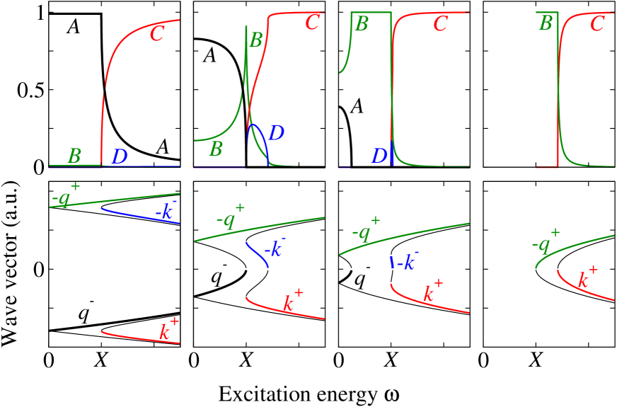
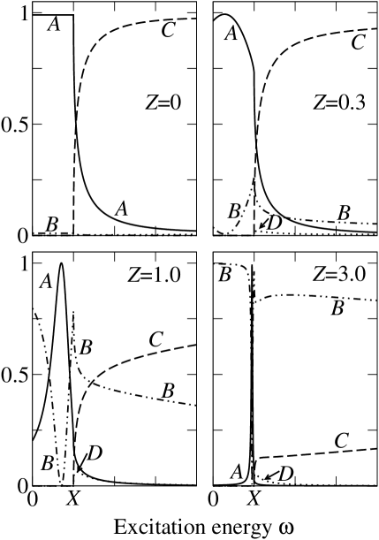
Figure 4 shows transmission and reflection coefficients vs. the excitation energy (upper row) for increasing values of the band gap : more precisely, we vary the ratio by keeping fixed and varying . We go from a wide-overlap semimetal () up to a small-gap semiconductor (). In the latter case we allow to be positive (SC/SC junction). In the lower row of Fig. 4 the dispersion relations for wave vectors of transmitted and reflected fluxes of the upper row are depicted, in the form () vs. . ’s (’s) stand for wave vectors of carriers on the SM (SC) side: a color code links spectrum branches (bottom row) with corresponding probability coefficients (top row). Data are obtained numerically, , and . When (left column, ), is almost one for , then slowly decreases as . Since and are negligible, and therefore strongly depends on , slowly increasing with energy as decreases. Sub-gap interband -reflection is totally dominant and dramatically affects the transport above the gap as well, while intraband -scattering is negligible. When increases, assuming values we unambiguosly associate to the heterogeneous junction (, second column), the interband -process is dramatically suppressed, both in weight and energy range. We note that -reflection is defined only when conduction and valence bands overlap on the SM side, namely for . Here , and therefore one would expect, for continuity, that the -probability were suppressed limitedly to the region where the overlap disappears, . Instead, is depleted over the whole allowed energy range, , suggesting that interband scattering is suppressed in the heterogeneous junction. Significantly, now both and channels are active, while the -transmission has a sharp dependence on energy only in a very small range, above which is practically constant and close to unity. If we sum together the weights of the two possible transmission channels, and , we see that the transmission probability is almost one for all energies above the gap. This is clearer at large (, third column): the weight of is less than 0.5 for , while for the system shows only ordinary -reflection and, above the gap (), almost unit -transmission. Eventually we approach the semiconductor scenario (right column, ), where the channel is absent as well as ( is complex), and transmission shows an almost featureless behavior, being approximately one above the gap and zero below. To sum up, Fig. 4 shows that, contrary to the case, transmission across the SM/NSC junction is basically featureless and dominated by sub-gap intraband reflection.
The previous results for small values of (left column of Fig. 4) are still consistent with both the homogeneous and heterogeneous cases. Therefore, in order to differentiate the two cases, we further consider the possibility of band offset at the interface, i.e. and , which is solely attributable to the heterogeneous junction. Figure 5 displays the -reflection probability vs. ( and ) for several values of the band energy offset at the interface, . The reflection probability, for , is simply . Here we consider a negative offset, namely SM bands are shifted downwards with respect to SC bands; different curves from up to down correspond to , 0.4, 0.6, 0.8, 0.9, 0.978, 0.98, 0.99, respectively. We see a clear suppression of the channel as long as the energy band displacement is increased. The two limiting cases correspond to , namely there is no displacement (see top inset of Fig. 5), and to , i.e. the top of SM valence band is exactly in line with the chemical potential (bottom inset of Fig. 5); the latter limit is the treshold beyond which interband reflection is forbidden. A priori one would expect strong suppression of the channel only close to the forbidden region, . Results instead show that the -weight is depleted all over the allowed energy range. This observation is consistent with the behavior of the heterogeneous junction for or larger we discussed above (Fig. 4). Since the band offset characterizes the heterogeneous junction only, we conclude that for a heterogeneous interface the -channel dominates with respect to .
The discussion is still incomplete, since the appearance of a band offset is itself a hallmark of the heterogeneous junction, but not the only one. However, the presence of any type of localized disorder at the interface (impurities, defects, surface states, insulating layers, etc.) universally characterizes the heterogeneous junction. Therefore, we explore the case and . Figure 6 shows how the dependence of transmission and reflection coefficients on the carrier energy evolves as a function of the barrier strength (, and ). When the interface is clean (, left top panel) almost all particles below the gap () are reflected with band changing, the probability of intraband reflection being approximately zero (, ). Immediately above the gap is still very close to one, decreasing with energy in an unexpectedly slow manner, while increases accordingly to (). As disorder is added to the interface, the probability of channel is dramatically suppressed (Fig. 6). Already a small amount of disorder (, top right panel of Fig. 6) is enough to significantly decrease the -reflection probability close to the gap, while the probabilities of -reflection and -transmission acquire a not negligible value. The disorder modifies probability coefficients, its effect strongly depending on (see e.g. plots for and in the bottom left panel of Fig. 6, at ). At the interband reflection is completely suppressed, except in a vanishingly small interval close to the gap, and the prevailing process is the ordinary intraband -reflection, whose weight is almost uniform over the entire energy range (bottom right panel of Fig. 6). At high values of , the effect of disorder is just to lower the transmission probability in an uniform manner (therefore increasing ), regardless of energy, acting as an additional scattering source to the featureless contact resistance of the interface. In this regime only intraband scattering is present.
We are now in the position to make a general statement on the comparison between homogeneous and heterogeneous junctions. We have seen in this section that in all physical cases characterizing the heterogeneous interface, namely comparable or larger that , and/or presence of band offset and disorder, the interband reflection is suppressed in favor of the intraband channel. The opposite holds for the homogeneous junction, where the channel dominates.
Appendix D Junction between semimetal and excitonic insulator
We now explore the physics of interband scattering, and discard the case of the SC gap originating from band hybridization, which is ordinary and uninteresting. Therefore, we take and .
We generalize the model to three dimensions, considering as an examplar case a planar interface between a semimetal and an excitonic insulator, with , namely the pairing is a contact interaction due to the fairly effective carrier screening in the semimetal. Here is a smooth increasing function of , tending respectively to the asymptotic values zero when , well inside the bulk semimetal, and to the constant when , inside the bulk EI [Fig. 2(a)]. Let be complex in this section. If the characteristic scale of the spatial variation of is much larger than the de Broglie wavelength of carriers, the local quasi-particle dispersion relation is
| (37) |
as schematically shown in Fig. 2(a). The quasi-particle excitations across the interface must satisfy the equations (1) of the main text, obtained by Eqs. (18) by putting . Equations (1) of main text are formally identical to those for bogoliubons in the intermediate state of a superconductor. Let us now apply the method of Andreev Andreev in considering the reflection of quasi-particles from the boundary separating the two phases.
The medium under consideration is completely homogeneous with an accuracy . Therefore, since (cf. App. C), we seek a solution of Eqs. (1) of main text in the form
| (38) |
where is some unit vector and and are functions that vary slowly compared to . Substituting (38) in (1) of main text and neglecting higher derivatives of and , we obtain
| (39a) | |||||
| (39b) | |||||
where . We find the asymptotic form of the solutions of Eqs. (39) describing the reflection of quasi-particles falling on the boundary of the semimetallic phase when . When we can put . Then
| (40) |
where , ; and are arbitrary constants. The first term on the rhs of Eq. (40) corresponds to a conduction band electron whose velocity (or ) lies along , and the second term to a valence band electron whose velocity lies in the opposite direction to (in fact since ). If , then the wavefunction (40) describes an electron of the conduction band incident on the boundary and reflected into the valence band on the semimetal side; if , it describes an incident valence-band electron reflected into the conduction band. Equations (38) and (40) provide the basis set used in Eq. (2) of the main text.
We must put in Eqs. (39) as . The solution describing the transmitted wave () has for the form
| (41) |
where is a constant, is the phase of the complex number ,
| (42a) | |||||
| (42b) | |||||
If , then the functions and decay exponentially as .
| No condensate () | ||||
| General form | ||||
| No barrier () | ||||
| Strong barrier [] | ||||
| 111There is a mistake in the corresponding result for a metal/superconductor junction appearing in Table II of Ref. BTK . | ||||
D.1 Coherence factors in the transmission coefficient
We show that the ratio of incident electrons which are transmitted through the interface [Eq. (3) of the main text] depends on the coherence factors of the condensate and is strongly suppressed close to the gap. Let us go back to the one-dimensional case and apply the boundary conditions to wavefunctions (35): we obtain an analytic solution if we let , which is reasonable since (“Andreev approximation”). We find
| (43) |
In the Andreev approximation, the probability coefficients are actually the currents, measured in units of . For example, , and . The expression for the energy dependences of , , , and can be conveniently written in terms of and , the coherence factors and evaluated on the branch outside the Fermi surface. The results obtained in the Andreev approximation are given in Table 1. For convenience, in addition to the general results we also list the limiting forms of the results for zero barrier () and for a strong barrier [], as well as for (the semimetal case).
Remarkably, the overall set of results of Table 1 is formally identical to the analogous quantities obtained for a metal / superconductor interface (e.g. compare with Table II of Ref. BTK ), the only slight difference being the behavior for . This is no coincidence: the appearance of coherence factors and in probability coefficients demonstrates that the electron-hole condensate strongly affects the transport and in general the wavefunction of carriers, by means of both inducing coherence on the SM side and altering transmission features.
References
- (1) L. V. Keldysh, in Bose-Einstein Condensation, edited by A. Griffin, D. W. Snoke, S. Stringari (Cambridge, Cambridge, 1996), pp. 246-280.
- (2) B. I. Halperin and T. M. Rice, Solid State Phys. 21, 115 (1968).
- (3) S. A. Moskalenko and D. Snoke, Bose Einstein Condensation of Excitons and Biexcitons (Cambridge, Cambridge, 2001), § 10.3.
- (4) B. Bucher, P. Steiner, and P. Wachter, Phys. Rev. Lett. 67, 2717 (1991).
- (5) L. V. Butov et al., Nature 417, 47 (2002).
- (6) R. R. Guseĭnov and L. V. Keldysh, Zh. Eksperim. Teor. Fiz. 63, 2255 (1972) [English transl.: Soviet Phys.–JETP 36, 1193 (1973)].
- (7) If a Schottky barrier is present at the interface, there is an abrupt jump in potential and the transport behavior belongs to the heterojunction class.
- (8) L. J. Sham and M. Nakayama, Phys. Rev. B 20, 734 (1979).
- (9) A. F. Andreev, Zh. Eksperim. Teor. Fiz. 46, 1823 (1964) [English transl.: Soviet Phys.–JETP 19, 1228 (1964)].
- (10) G. E. Blonder, M. Tinkham, and T. M. Klapwijk, Phys. Rev. B 25, 4515 (1982).
- (11) A. M. Zagoskin, Quantum Theory of Many-Body Systems (Springer, New York, 1998), § 4.5.1.
- (12) M. Rontani and L. J. Sham, Appl. Phys. Lett. 77, 3033 (2000).
- (13) M. Rontani and L. J. Sham, cond-mat/0309687.
- (14) J. M. Ziman, Electrons and Phonons (Oxford, London, 1960).
- (15) D. V. Khveshchenko, Phys. Rev. Lett. 87, 246802 (2001).
- (16) S. Datta, M. R. Melloch, and R. L. Gunshor, Phys. Rev. B 32, 2607 (1985).
- (17) A. L. Kasatkin and E. A. Pashitskii, Sov. J. Low Temp. Phys. 10, 640 (1984); M. I. Visscher and G. E. W. Bauer, Phys. Rev. B 54, 2798 (1996); S. N. Artemenko and S. V. Remizov, JETP Lett. 65, 53 (1997).
- (18) D. Jérome, T. M. Rice, and W. Kohn, Phys. Rev. 158, 462 (1967).
- (19) L. V. Keldysh and Yu. V. Kopaev, Fiz. Tverd. Tela 6, 2791 (1964) [English transl.: Soviet Phys.–Solid State 6, 2219 (1965)].
- (20) T. Portengen, Th. Östreich, and L. J. Sham, Phys. Rev. Lett. 76, 3384 (1996).
- (21) T. Portengen, Th. Östreich, and L. J. Sham, Phys. Rev. B 54, 17452 (1996).
- (22) J.-M. Duan, D. P. Arovas, and L. J. Sham, Phys. Rev. Lett. 79, 2097 (1997).
- (23) A. A. Abrikosov, L. P. Gorkov, and I. E. Dzyaloshinski, Methods of Quantum Field Theory in Statistical Physics (Dover, New York, 1975), § 8.1.
- (24) Here, in defining the probability density and, consequently, the probability current , we consider only the intra-band free-carrier contribution. However, we could as well have included in the definition of also the inter-band contribution of the atomic polarization: . This would add to the current an additional diamagnetic term whose average value in any eigenstate of the Hamiltonian of Eq. (5) is zero, as discussed by Nozières and Saint-James notecurrent2 .
- (25) P. Nozières and D. Saint-James, J. Physique - Lettres 41, L-197 (1980).
- (26) W. Kohn and D. Sherrington, Rev. Mod. Phys. 42, 1 (1970).
- (27) J. Zittartz, Phys. Rev. 164, 575 (1967).
- (28) The authors define SN the interface potential as the residual part of the potential once that an ideal lattice discontinuity (“flat-band condition”) has been included in the unperturbed solution.
- (29) The latter boundary condition differs in sign from the one appropriate to the metal/superconductor junction, as outlined in Ref. BTK .
- (30) A. N. Kozlov and L. A. Maksimov, Zh. Eksp. Teor. Fiz. 48, 1184 (1965) [English transl.: Soviet Phys.–JETP 21, 790 (1965)].