Models of Electrodes and Contacts in Molecular Electronics
Abstract
Bridging the difference in atomic structure between experiments and theoretical calculations and exploring quantum confinement effects in thin electrodes (leads) are both important issues in molecular electronics. To address these issues, we report here, by using Au-benzenedithiol-Au as a model system, systematic investigations of different models for the leads and the lead-molecule contacts: leads with different cross-sections, leads consisting of infinite surfaces, and surface leads with a local nanowire or atomic chain of different lengths. The method adopted is a non-equilibrium Green function approach combined with density functional theory calculations for the electronic structure and transport, in which the leads and molecule are treated on the same footing. It is shown that leads with a small cross-section will lead to large oscillations in the transmission function, , which depend significantly on the lead structure (orientation) because of quantum waveguide effects. This oscillation slowly decays as the lead width increases, with the average approaching the limit given by infinite surface leads. Local nanowire structures around the contacts induce moderate fluctuations in , while a Au atomic chain (including a single Au apex atom) at each contact leads to a significant conductance resonance.
pacs:
73.40.Cg, 72.10.-d, 85.65.+hI Introduction
To have precise control over the atomic structure of individual molecular devices, which consist of, at least, a molecule and two electrodes used as leads of electronic current, is one of the major challenges in molecular electronics. In recent experiments on electron transport through single molecule devices, a break junction is a commonly used technique for building a lead-molecule-lead (LML) system. A break junction can be constructed either through electromigration morpurgo1 ; park ; morpurgo2 ; fuhrer or through the mechanically controllable break junction (MCB) technique bj1 ; bj2 ; bj3 ; h2 . In the MCB technique a metal wire is elongated and broken by the bending of the substrate, and therefore the resulting break gap can be controlled by adjusting the bending, providing a flexibility for controlling the device structure. In all these break junction experiments, the detailed atomic structure of the molecule-lead contacts is not available and so neither is its influence on the transport properties of the device. However, some information about the main features of the contact atomic structure has been revealed in MCB experiments. It has been shown that well before a metal wire breaks a very thin bridge region is formed which contributes only several (=, conductance quantum) of conductance to the wire h2 ; wire . This means that in a real MCB LML system the molecule is usually connected to a very thin nanowire which is then connected to the extended part of the metal lead.
Other experimental approaches for constructing well defined lead/single-molecule/lead systems involve the use of chemical self-assembly of molecules on surfaces and/or direct atomic manipulation using scanning tunneling microscopy (STM) or atomic-force microscopy (AFM) (surface-STM/AFM technique) Datta972530 ; Cui01571 ; Xiao04267 . In these experiments one of the leads is an infinite large surface (the substrate surface) and the other one (the STM or AFM tip) can also be approximately regarded as a large surface but with a local structure at the contact. In the case of pulling the tip away from the surface, a single apex atom connection or single atomic chain connection may develop at the contacts, as has been shown experimentally Xiao04267 ; Ohnishi ; Yanson . Similar to this situation, a recent experiment au-chain showed that by using directly STM atomic manipulation on NiAl(110) surface one can assemble LML systems with precise contact atomic structures, in which single gold atomic chains can be used as leads.
On the other hand, in future molecular electronics circuits, the interconnects should be comparable in size to the functional devices and the best choice may be some kind of one dimensional (1D) nanostructures. Recent experiments have shown that 1D nanostructures like carbon nanotubes Mceuen04272 ; Heer04281 ; Avouris04403 or semiconductor nanowires Yang02553 ; Melosh03112 ; Beckman045921 are potentially ideal building blocks for functional devices and interconnects in nanoelectronics. Their size can be as small as 1 nm sinw1nm ; cnt3a . From the different experimental situations mentioned above, one can see the wide variety of lead and contact structures and the significance of leads (interconnects) with a nanometer diameter in future molecular electronics technologies.
With regard to theoretical modeling, a metal lead can be modeled by either an infinite surface (for example, Refs. infinite-lead-1, ; infinite-lead-2, ; infinite-lead-3, ; diventra0, ; diventra1, ; diventra2, ) or a very thin atomic wire (for example, Refs. nanowire-lead, and ourwork1, ; ourwork2, ). The infinite-surface–lead model is relevant to surface-STM/AFM experiments without the pulling of the tip, while the thin atomic wire model is appropriate for the possible nanowire or even atomic-chain interconnects in molecular electronics circuits. On the other hand, the situation in MCB experiments or surface-STM/AFM experiments, where a very thin nanowire connection or single atomic chain connection is developed, is between these two theoretical limits.
For a LML system with nanowire leads or connections around its contacts, the behavior of the electron transport through the whole system will not only depend on the molecule and contacts but also on the metallic lead itself, in which quantum confinement effects will become significant because of its small cross-section. In addition, for leads with a regular periodic structure, there will be a strong quantum waveguide effect. This thin lead induced effect may be important for understanding relevant experiments and for reasonable comparisons between theoretical calculations and experiments. However, it has been unclear what the detailed effect is and how significant it can be on the electron transport. The main reason for this lack of understanding is that, to date, there have been no calculations on electron transport through LML systems with leads of different widths, from a thin wire to an infinite surface, in a consistent manner, and therefore, there have been no theoretical analyses available concerning quantum confinement effects in thin leads compared to infinite surface leads.
(a)
 (b)
(b)
 (c)
(c)
 (d)
(d)
 (e)
(e)
 (f)
(f)
In this paper, we focus on exploring quantum confinement effects in leads with a finite cross-section and on bridging the difference in contact atomic structure between MCB or surface-STM/AFM experiments and theoretical calculations. For these purposes, we carry out first-principles calculations of molecular conductance of a Au-benzenedithiol-Au system adopting different atomic models for the leads and contacts. Our strategy is to bring the two theoretical limits together: We adopt a reliable model for the infinite surface leads and use the result as a limit/reference to which the results from systems with leads of different finite cross-sections are compared. Therefore, we consider the following models for the lead: (1) (001) and (111) gold nanowires with different widths and (2) infinite periodic Au(001) and Au(111) surfaces. Furthermore, the nanowire structures that develop around the lead-molecule contacts revealed in MCB experiments are simulated by introducing a nanowire of varying length between the molecule and the infinite periodic surface. Similarly, the single apex atom or single atomic chain connections that occur in the surface-STM/AFM experiments are also simulated by introducing a single Au atomic chain at each contact.
Our calculations show that a small cross-section lead causes large oscillations in the electron transmission function [] because of waveguide effects, and therefore this effect depends significantly on the lead structure, such as different lead orientations. This oscillation slowly decays along with the increase of the lead width, with the average approaching the limit given by the corresponding infinite surface lead, for which the effect of different lead orientations is significantly reduced. The local nanowire structure around the contacts induces moderate fluctuations in , keeping the main features unchanged if the nanowire is not too long. In contrast to this, the Au atomic chain (including single apex Au atom) connection at each contact leads to a more significant resonance in the equilibrium conductance. Based on the above findings, together with some previous theoretical results, we discuss the relationship between ab initio theory and experiment in molecular electronics. It is shown that for different contact structures theoretical predictions of conductance are always much larger than relevant experimental results, which has become an important issue in molecular electronics and needs to be addressed by further work.
II Modeling and computation
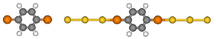
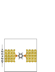
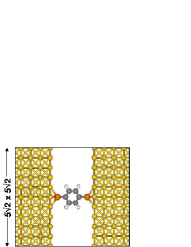
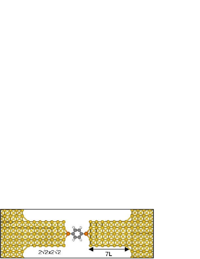
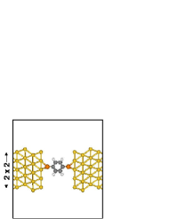
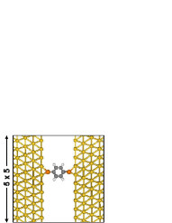
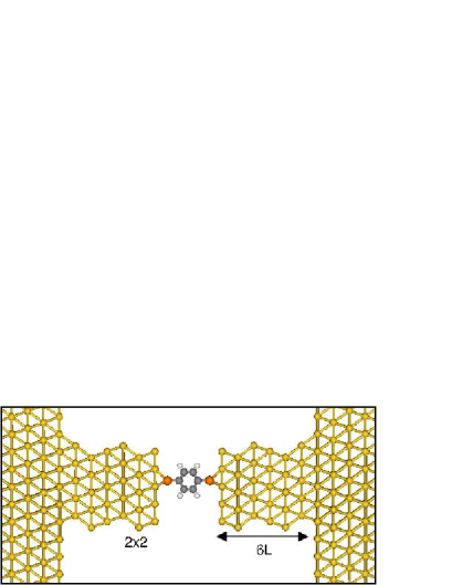
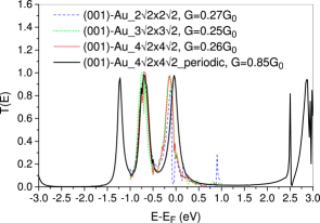
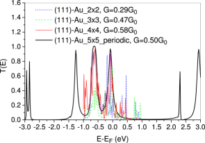
We consider different models for the leads and lead-molecule contacts of a Au-benzenedithiol-Au system: (A) leads with different finite cross-sections, (B) leads of infinite periodic surfaces, (C) periodic surface leads with a nanowire connection of different lengths to the molecule, and (D) similar to (C) but with a single atomic chain (including a single apex atom) at the contacts. Two lead orientations, (001) and (111), are considered. Examples of atomic structure of the device regions in the different models are shown in Fig. 1. Fig. 1 (a) shows the atomic structure of a device region in Model A for the (001) orientation, which has leads with a finite cross-section, 2. Fig. 1 (b) is a (001) system in Model B, which has leads of 5 periodic surface. Fig. 1 (c) shows the device region of a (001) system in Model C, where a 7-atomic-layer 2 nanowire is introduced to connect the molecule to the 4 periodic surface lead, to simulate the possible experimental situations in MCB experiments mentioned previously. Figs. 1 (d) – (f) show the atomic structures of the counterparts for the (111) lead orientation. For all the structures the Au-Au bond length in the leads is fixed at 2.89 Å (i.e., experimental bulk bond length) and the molecules are adsorbed at the hollow site of the Au(001) or Au(111) surface with the molecule-surface separation optimized. As can be seen in Fig. 1, we adopt very large supercells for Model B. Because of the large separation between the molecule and its images (larger than 12Å), the interference among supercells will be very small; therefore, this model is a good approximation to a lead consisting of an infinitely large surface, as we will demonstrate later. The single atomic chain connection in Model D is equivalent to changing the molecule from S-C6H4-S to Aun-S-C6H4-S-Aun, as shown in Fig. 2, where a 3-Au-atom-chain (=3) is attached on each side. We consider = 1, 2, and 3 in our calculation for Model D.
We adopt a nonequilibrium Green function (NEGF) negf1 ; negf2 method combined with density functional theory (DFT) dft2 electronic structure calculations to investigate the electron transport datta1 ; datta2 ; pal1 ; mcdcal ; transiesta ; trank1 . Specifically,trank1 we divide an infinite LML system into three parts: left lead, right lead, and device region () which contains the molecule and large parts of the left and right leads (devices regions shown in Fig. 1), so that the molecule-lead interactions (couplings) can be fully accommodated. Unlike some other theoretical calculations adopting infinite surface leads infinite-lead-1 ; infinite-lead-2 ; infinite-lead-3 ; diventra0 ; diventra1 ; diventra2 in which the device region and leads are treated on different theoretical levels, here all the subsystems are treated on exactly the same footing. For a steady state situation in which region is under a bias (zero or finite), its density matrix () and Hamiltonian () can be determined self-consistently by DFT+NEGF techniques datta1 ; datta2 ; pal1 ; mcdcal ; transiesta ; trank1 . The Kohn-Sham wave-functions are used to construct a single-particle Green function from which the transmission coefficient at any energy is calculated. The conductance, , then follows from a Landauer-type relation. The detailed computational techniques have been described previously trank1 .
For the electronic structure calculation, we use DFT and adopt a numerical basis set to expand the wave functions siesta . A single zeta plus polarization basis set (SZP) is adopted for all atomic species. Our test calculation for a small system shows that the result of the SZP calculation has only minor differences from that of a calculation using a higher level double zeta plus polarization basis set (DZP). We make use of optimized Troullier-Martins pseudopotentials tmpp for the atomic cores. The PBE version of the generalized gradient approximation (GGA) pbe is used for the electron exchange and correlation. The atomic structure of the isolated molecule and the molecule-lead separation are fully optimized using the higher level DZP basis set.
III Leads: finite and infinite cross-section
(a)
 (b)
(b)
As has been mentioned previously, the use of nanowire leads with small cross sections in molecular electronics or nanoelectronics is very promising. Therefore, it is important to investigate its possible consequences. So far it has been unclear what the effect of a very thin lead is and how significant it can be on the electron transport through the LML system. Here we investigate this issue by calculating the electron transmission adopting Model A with different lead widths in comparison with Model B.
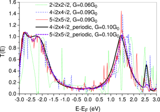
In Figs. 3 (a) and (b) we show for Models A and B for the (001) and (111) lead orientations, respectively. In Model B we use a periodic surface lead to simulate an infinitely large surface lead. Obviously, for this purpose we have the issue of convergence of the in-plane size of the supercell. If the size is small the molecule will interact with its images and the result will vary remarkably with the increasing size. Here we adopt a very large in-plane size [() for the (001) orientation and for the (111)], as a result, the direct inter-molecule interactions have been completely removed because of the large inter-molecule separation ( 12 Å ) and the use of the basis functions with a finite range. In order to check the convergence we compare the result of from the surface lead to that from an even larger surface lead. ¿From the results in Fig. 3 (a) we see that the two curves are very close to each other, indicating that the in-plane size of these periodic surface leads is already large enough to simulate an infinitely large surface lead.
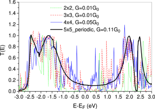
Fig. 3 (a) shows that the function of Model A depends strongly on its lead width. The small cross-section, , leads to large sharp oscillations in the function. Along with the increase of the lead width to and , the amplitude of this oscillation decays and a large-scale structure appears, whose average is approaching the limit given by the periodic surface leads. In spite of the overall large difference in between Model B and Model A with thin leads, the difference in their equilibrium conductance is quite small for the (001) orientation.
The results for the (111) lead orientation are summarized in Fig. 3 (b). Here the oscillations in for Model A are even much larger than those in the (001) case and the convergence with the lead width is much slower: even the result given by the lead with cross-section does not show the large-scale structure given by the periodic surface lead. Related to this much stronger oscillation, here the equilibrium conductance given by Model A is significantly smaller (by about one order of magnitude) than that given by Model B, in contrast to the (001) case. An interesting thing to notice is that although in Model A the functions for the (001) and (111) orientations are very different, they become similar in Model B, as shown by the solid lines in Fig. 3. The only major difference is in the relative position of the Fermi energy in the gap, which is a result of the different charge transfer around the (001) and (111) contacts.

The large oscillations in function given by Model A for both the (001) and (111) lead orientations can be understood by considering the waveguide effect of the leads. In Model A the leads are infinitely long periodic nanowires. As a result of the transversal quantum confinement and the periodic structure, the electron transmission coefficient through these leads is always an integer. However, because of their complicated atomic structure the transverse modes in these 1D waveguides will have a complicated dependence on the electron energy, resulting in sharp step-function oscillations in their functions. To show this clearly, we calculate for the pure infinitely long (111) lead with 3 cross section. The result in Fig. 4 clearly shows the expected large step-function oscillation. After scattering by the molecule, this strongly oscillating transverse mode spectra will cause large oscillations in the projected density of states (PDOS) on the molecule, as shown in Fig. 5. Obviously, this oscillating PDOS combined with the molecule-lead coupling will give a strongly oscillating spectra for the whole LML system, as we already see in Fig. 3 (b). The behavior of a nanowire waveguide will depend critically on its cross-section atomic structure. Because the (111) nanowire leads are more irregular in atomic structure and have much lower symmetry than the (001) nanowire leads, the oscillations in the of the (111) LML systems will be stronger and the convergence with respect to the lead width will be slower compared to the (001) case, as can be seen by comparing Figs. 3 (a) and (b).

As the lead gets wider, the number of the transverse modes in the lead increases, and in addition, the number of modes that are coupled to the molecule also increases. At the same time, the average transmission through the whole system remains the same. Thus the transmission from a given mode in the lead through the molecule will go down. Hence the threshold singularity associated with that mode will also decrease. Therefore, as the lead gets wider and wider, the oscillation structure in the full T(E) should become both smaller and finer. However, this expected decay is not so clear when we increase the width of the (001) lead from to and that of the (111) lead from to (see Fig. 3). This indicates that (1) this kind of decay is slow and the cross-section of the leads used in our calculations is still too small to clearly show it, and therefore (2) this quantum waveguide effect may be measurable for real nanometer-sized leads/interconnects in molecular electronics.
(a)
 (b)
(b)
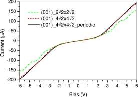
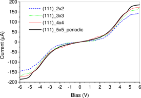
The large oscillations in of Model A may also have some effects on its - characteristics. To show the possible effects while avoiding the too large computational cost due to the different large lead widths, we calculate the - curves directly from the functions in Fig. 3, i.e., bias-induced changes in are neglected. The results given in Fig. 6 show that despite the significant dependence of on the structure and cross-section of the leads in Model A, the - characteristic is not so sensitive to these factors: even for very thin nanowire leads the main feature of the - characteristic has already been captured.
IV Nanowire connection around the contacts
(a)
 (b)
(b)
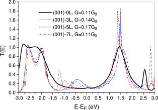
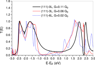
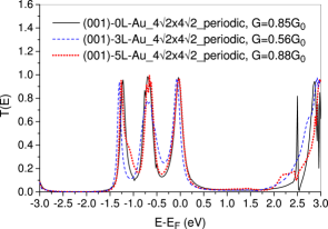
While having been adopted extensively in previous theoretical calculations, leads with a tiny cross-section nanowire-lead ; ourwork1 ; ourwork2 ; trank1 and with an infinite cross-section infinite-lead-1 ; infinite-lead-2 ; infinite-lead-3 ; diventra0 ; diventra1 ; diventra2 are the two theoretical limits, which correspond to the Model A and Model B, respectively, in this paper. The real situation in MCB experiments is probably between these two, where a finite-length nanowire is usually developed connecting the molecule to the extended electrode of a LML system. To simulate this situation, here we consider a nanowire with different lengths, which connects the benzene molecule to an infinite periodic surface (i.e., Model C). The cross-section of the nanowire is set to be for the (001) system and for the (111) system. The atomic structures of these systems are shown in Fig. 1 (c) and (f), where the length of the nanowire is denoted by the number of atomic layers it contains (i.e., 7L means a nanowire consisting of 7 atomic layers).
The calculated functions are shown in Fig. 7. As can be seen, the introduction of the nanowire connection around the contacts causes noticeable changes in transmission coefficient over the whole energy range. This is because the finite-length nanowire depresses some transverse modes and enhances some others. In spite of this, the main feature of the functions still remains for the lengths of the nanowires studied here. Keeping the behavior of Model A in mind, one can image that, along with the increase of the length of the nanowire, the induced fluctuation in will become larger and larger. This is just the case as we can see in Fig. 7, especially for the (111) system. Also similar to Model A, here the (111) nanowire induces more fluctuation than the (001) nanowire does, especially in the equilibrium conductance as listed in the legends of Fig. 7.
V Effects of atomic chain connections around the contacts
(a)
 (b)
(b)
 (c)
(c)
Besides the large scale changes in atomic structure that we have discussed above, there are other possibly more localized changes around contacts in MCB experiments. One is atomic fluctuation (roughness) of the break surfaces, and as a result, a molecule may be connected through an apex atom rather directly to the flat surface. In surface-STM/AFM experiments, if we pull the tip away from the surface a single apex connection or a single atomic chain connection will develop Xiao04267 ; Ohnishi ; Yanson . Here we simulate this situation by adding a Au atomic chain, Aun (= 1, 2, and 3), at each contact between the molecule and the infinite surface lead.

First, let us look at the case of which means an additional apex Au atom at each contact. For the systems with small leads (Model A) its effect was previously investigated ourwork1 ; ourwork2 . It was found that presence of the additional Au atoms increases significantly the equilibrium conductance due to a resonance caused by a molecular level aligned with the Au Fermi energy. Here we further investigate the effect for Models B and C, and to check if the conclusion is affected by the strong oscillating behavior of Model A.
In Fig. 8 we show functions for Models A, B, and C. The introduction of the additional Au atom changes totally the functions and leads to a large resonance peak around the Fermi energy for all the different models, independent of the different structures in each model. Thus, the conclusion about the effect of the additional Au atom, which was reached previously for Model A with small lead widths ourwork1 ; ourwork2 , is a general result regardless of the lead and contact structures.
For Model A in the (001) orientation, Fig. 8 (a) shows that the additional Au atom stabilizes the structure even for the smallest lead width, and the result of Model A converges quickly to that of Model B. For Model A in the (111) orientation, this effect also exists but is weaker, as shown in Figs. 8 (c), because of the much stronger oscillating behavior. For all the different structures in Models B and C, including the different lead orientations and the different lengths of connecting nanowire in Model C, the introduction of the additional Au atom changes totally and leads to very similar results. This indicates that in this system it is the local change in contact structure that is important in determining the transport properties of the whole LML system.
The results for =2 and 3 are given in Fig. 9. The increase in the length of the Au atomic chain narrows the peaks in , keeping the main feature unchanged except for a new peak around -2.5 eV for =2 or -1.7 eV for =3. The large resonance peak around the Fermi energy remains although its height is reduced as increases.
These results are particularly interesting in light of the experiments and conclusions of Ref. Xiao04267 . There measurements of the conductance through single molecules of benzenedithiol and benzenedimethanethiol by using a STM technique were reported. The conductance found was much larger than previous experimental results bj1 . The paper goes on to state that the new results are in agreement with theoretical expectations, citing Ref. diventra1, . The claimed agreement with theory is quite significant because the big discrepancy in conductance between ab initio theory diventra0 ; diventra1 ; diventra2 ; taylor03 ; infinite-lead-1 ; ourwork1 and experiments bj1 ; zhou97 ; reichert03 ; kubatkin03 ; rawlett02 ; kushmerick03 (about two orders of magnitude) is a long standing issue in the field of molecular electronics.
The experiment of Ref. Xiao04267, differs from previous ones in that additional gold atoms may be present at the molecule-gold contact. The paper states that the distance over which a molecular junction can be stretched for both benzenedithiol and benzenedimethanethiol is between 0.3 and 0.6 nm. This distance is not how long the molecules themselves are stretched but rather is due to reconfiguration of the gold contacts: When a gold atom at the molecule-gold contact is pulled out of the electrode, a nearby surface gold atom moves behind the first atom. Further pulling can cause a third atom to move behind the second one and form a linear atomic chain. Based on this observation and analysis, the authors suggest that the molecule is connected to the electrode through an apex Au atom. Indeed, 0.3 nm is in very good agreement with the distance change due to one apex Au atom at each of the two contacts.
The theoretical configuration for comparison should certainly take into account the molecule-metal contact region, and, in particular, must include an apex Au atom. The work used for comparison diventra1 , however, did not include an apex Au atom and used the jellium model for the electrodes which does not give a good account of the molecule-metal contact region.
Comparing the experimental results of Ref. Xiao04267, with the results of this Section, we find that the experimental value is still much smaller than the theoretical results, by one to two orders of magnitude. Therefore the long standing discrepancy between experiment and theory remains, and urgently needs to be addressed by further work.
VI Summary
In an effort to explore the effect of a small lead cross-section and to bridge the difference in atomic structure between experiment and theory, we have investigated different models for the lead and contact structures of a Au-benzenedithiol-Au system: leads with different finite cross-sections, leads consisting of infinite surfaces, and surface leads with a local nanowire or a single atomic chain connecting the molecule. The findings are as follows:
(1) Waveguide effects in leads with a small cross-section will lead to large sharp oscillations in the function, which depend significantly on the lead structure (orientation). These oscillations slowly get smaller as the lead width increases, with the average approaching the limit given by the infinite surface leads, for which the effect of different lead structures is significantly reduced. The effect of this strong oscillation on - characteristics is, however, relatively weak.
(2) The local nanowire structure around the contacts will induce noticeable fluctuations in function. However, the main feature of the function will remain if the nanowire structure is not too long, as those considered in this paper.
(3) In contrast to the above effect, the single atomic chain (including a single apex atom) at each contact leads to a large robust resonance in the conductance.
We appreciate valuable conversations with Rui Liu. This work was supported in part by the NSF (DMR-0103003).
References
- (1) A.F. Morpurgo, C.M. Marcus, and D.B. Robinson, Appl. Phys. Lett. 74, 2084 (1999).
- (2) H. Park, A.K.L Lim, A.P. Alivisatos, J. Park and P.L. McEuen, Appl. Phys. Lett. 75, 301 (1999).
- (3) Y.V. Kervennic, H.S.J. Van der Zant, A.F. Morpurgo, L. Gurevich, L.P. Kouwenhoven, Appl. Phys. Lett. 80, 321 (2002).
- (4) M.S. Fuhrer (private communication).
- (5) M.A. Reed, C. Zhou, C.J. Muller, T.P. Burgin, and J.M. Tour, Science 278, 252 (1997).
- (6) C. Kergueris, J.P. Bourgoin, S. Palacin, D. Esteve, C. Urbina, M. Magoga, and C. Joachim, Phys. Rev. B 59, 12505 (1999).
- (7) J. Reichert, R. Ochs, D. Beckmann, H.B. Weber, M. Mayor, and H.v. Löhneysen, Phys. Rev. Lett. 88, 176804 (2002).
- (8) R.H.M. Smit, Y. Noat, C. Untiedt, N.D. Lang, M.C. van Hemert, and J.M. van Ruitenbeek, Nature 419, 906 (2002).
- (9) J.G. Rodrigo, A. García-Martín, J.J. Sáenz, and S. Vieira, Phys. Rev. Lett. 88, 246801 (2002).
- (10) S. Datta, W. Tian, S. Hong, R. Reifenberger, J.I. Henderson, and C.P. Kubiak, Phys. Rev. B 79, 2530 (1997).
- (11) X.D. Cui, A. Primak, X. Zarate, J. Tomfohr, O.F. Sankey, A.L. Moore, T.A. Moore, D. Gust, G. Harris, and S.M. Lindsay, Science 294, 571 (2001).
- (12) X.Y. Xiao, B.Q. Xu, N.J. Tao, Nano Lett. 4, 267 (2004).
- (13) H. Ohnishi, Y. Kondo, K. Takayanagi, Nature 395, 780 (1998).
- (14) A.I. Yanson, G. Rubio Bollinger, H.E. van den Brom, N. Agrait, and J.M. van Ruitenbeek, Nature 395, 783 (1998).
- (15) G.V. Nazin, X.H. Qiu, and W. Ho, Science 302, 77 (2003).
- (16) P.L. McEuen and J.Y. Park, Mat. Res. Soc. Bull. B 29, 272 (2004).
- (17) W.A. de Heer, Mat. Res. Soc. Bull. B 29, 281 (2004).
- (18) Ph. Avouris, Mat. Res. Soc. Bull. B 29, 403 (2004).
- (19) P. Yang, C.M. Lieber, and R. Kaltschmidt, Nature 419, 553 (2002).
- (20) N.A. Melosh, A. Boukai, F. Diana, B. Gerardot, A. Badolato, P.M. Petroff, and J.R. Heath, Science 300, 112 (2003).
- (21) R.A. Beckman, E. Johnston-Halperin, N.A. Melosh, Y. Luo, J.E. Green, and J.R. Heath, J. Appl. Phys. 96, 5921 (2004).
- (22) D.D.D. Ma, C.S. Lee, F.C.K. Au, S.Y. Tong, and S.T. Lee, Science 299, 1874 (2003).
- (23) X. Zhao, Y. Liu, S. Inoue, T. Suzuki, R. O. Jones, and Y. Ando, Phys. Rev. Lett. 92, 125502 (2004).
- (24) Y. Xue, S. Datta, and M. A. Ratner, J. Chem. Phys. 115, 4292 (2001); Y. Xue and M. A. Ratner, Phys. Rev. B 68, 115406 (2003); Y. Xue and M. A. Ratner, Phys. Rev. B 68, 115407 (2003).
- (25) J.J. Palacios, A.J. Prez-Jimnez, E. Louis, E. SanFabin, and J.A. Vergs, Phys. Rev. B 66, 035322 (2002); J.J. Palacios, A.J. Prez-Jimnez, E. Louis, E. SanFabin, and J.A. Vergs, Phys. Rev. Lett. 90, 106801 (2003).
- (26) N.D. Lang, Phys. Rev. B 52, 5335 (1995); N.D. Lang, Ph. Avouris, Phys. Rev. Lett. 84, 358 (2000); N.D. Lang, Ph. Avouris, Phys. Rev. B 64, 125323 (2001).
- (27) M. Di Ventra, S.T. Pantelides, N.D. Lang, Phys. Rev. Lett. 84, 979 (2000)
- (28) M. Di Ventra, S. G. Kim, S. T. Pantelides, N. D. Lang, Phys. Rev. Lett. 86, 288 (2001).
- (29) M. Di Ventra, N. D. Lang, S. T. Pantelides, Chem. Phys. 281, 189 (2002).
- (30) J. Taylor, H. Guo, and J. Wang, Phys. Rev. B 63, 121104(R) (2001); B. Larade, J. Taylor, H. Mehrez, and H. Guo, Phys. Rev. B 64, 075420 (2001); B. Larade, J. Taylor, Q.R. Zheng, H. Mehrez, P. Pomorski, and H. Guo, Phys. Rev. B 64, 195402 (2001); C. Roland, B. Larade, J. Taylor, and H. Guo, Phys. Rev. B 65, 041401 (2002); H. Mehrez, A. Wlasenko, B. Larade, J. Taylor, P. Grütter, and H. Guo, Phys. Rev. B 65, 195419 (2002); C. Roland, V. Meunier, B. Larade, and H. Guo, Phys. Rev. B 66, 035332 (2002); C.-C. Kaun, B. Larade, and H. Guo, Phys. Rev. B 67, 121411 (2003).
- (31) S.-H. Ke, H. U. Baranger, and W. Yang, J. Am. Chem. Soc. 126, 15897 (2004); J. Chem. Phys. 122, 074704 (2005).
- (32) R. Liu, S.-H. Ke, H. U. Baranger, and W. Yang, J. Chem. Phys. 122, 044703 (2005).
- (33) H. Haug and A.-P. Jauho, Quantum Kinetics in Transport and Optics of Semiconductors (Springer-Verlag, Berlin, 1996).
- (34) S. Datta, in Electronic Transport in Mesoscopic Systems, edited by H. Ahmed, M. Pepper, and A. Broers (Cambridge University Press, Cambridge, England, 1995).
- (35) R.G. Parr and W. Yang, Density-Functional Theory of Atoms and Molecules (Oxford University Press, New York, 1989).
- (36) J. Taylor, H. Guo, and J. Wang, Phys. Rev. B 63, 245407 (2001).
- (37) P.S. Damle, A.W. Ghosh, and S. Datta, Phys. Rev. B 64, 201403 (2001).
- (38) Y. Xue, S. Datta, and M.A. Ratner, Chem. Phys. 281, 151 (2002).
- (39) M. Brandbyge, J.-L. Mozos, P. Ordejón, J. Taylor, and K. Stokbro, Phys. Rev. B 65, 165401 (2002).
- (40) E. Louis, J.A. Vergs, J.J. Palacios, A.J. Prez-Jimnez, and E. SanFabin, Phys. Rev. B 67, 155321 (2003).
- (41) S.-H. Ke, H. U. Baranger, and W. Yang, Phys. Rev. B 70, 085410 (2004).
- (42) J.M. Soler, E. Artacho, J.D. Gale, A. Garcia, J. Junquera, P. Ordejón, and D. Sánchez-Portal, J. Phys. C 14, 2745 (2002).
- (43) N. Troullier and J.L. Martins, Phys. Rev. B 43, 1993 (1991).
- (44) J.P. Perdew, K. Burke, and M. Ernzerhof, Phys. Rev. Lett. 77, 3865 (1996).
- (45) J. Taylor, M. Brandbyge, K. Stokbro, Phys. Rev. B 68, 121101(R) (2003).
- (46) J. Reichert, H. B. Weber, M. Mayor, and H. v. Löhneysen, Appl. Phys. Lett. 82, 4137 (2003).
- (47) S. Kubatkin, A. Danilov, M. Hjort, J. Cornil, J.-L. Brédas, N. Stuhr-Hansen, and P. Hedeg, Nature 425, 698 (2003).
- (48) A. M. Rawlett, T. J. Hopson, L. A. Nagahara, R. K. Tsui, G. K. Ramachandran, and S. M. Lindsay, Appl. Phys. Lett. 81, 3043 (2002).
- (49) C. Zhou, M. R. Deshpande, M. A. Reed, L. Jones II, and J. M. Tour, Appl. Phys. Lett. 71, 611 (1997).
- (50) J. G. Kushmerick, J. Naciri, J. C. Yang, R. Shashidhar, Nano Lett. 3, 897 (2003).