Metallic atomic wires on a patterned dihydrogeneted Si(001)
Abstract
Electronic structure calculations for atomic wire of metals like Al, Ga and In are performed for a patterned dihydrogeneted Si(001):1 1 in search of structures with metallic behavior. The dihydrogeneted Si(001) is patterned by depassivating hygrozen atoms only from one row of Si atoms along the [10] direction. Various structures of adsorbed metals and their electronic properties are examined. It is found that Al and Ga atomic wire structures with metallic property are strongly unstable towards the formation of buckled metal dimers leading to semiconducting behavior. Indium atomic wire, however, displays only marginal preference towards the formation of symmetric dimers staying close to the metallic limit. The reasons behind the lack of metallic atomic wires are explored. In addition, a direction is proposed for the realization of metallic wires on the dihydrogeneted Si(001).
pacs:
73.20.-r, 73.21.Hb, 73.90.+fI Introduction
The study of metals on semiconductors dates back to the nineteenth century and has seen a vigorous recent revival due to tremendous interest in Nanotechnology. The scanning tunneling microscopy has enabled us to manipulate atoms, place them at will on different surface sites to create exotic artificial atomic scale structures with novel electronic properties.hoso ; crom ; shen1 ; watb The placement of metal atoms such as Al, Ga and In on Si(001) may lead to the formation of low-dimensional structures shen2 , exhibiting significant new electronic and transport properties. Atomic scale structures themselves have technological applications in developing atomic scale devices. wada In particular, realization of a one dimensional metallic nanowire is of great importance because of its possible use as metallic interconnect in nano-devices.
There is much current activity in bottoms up approach where free standing atomic and nanowires for a variety of atoms, e.g., K, Al, Cu, Ni, Au and Si have been studied por ; por1 ; tor ; tak ; hak ; sen ; sen1 ; ipb1 . The geometrical structures of such free standing wires and their electronic properties have been discussed. A general finding is that a zigzag structure in the form of an equilateral triangle is most stable por ; por1 ; sen ; ipb1 . This can be understood as arising primarily due to the maximization of coordination number for each atom in a quasi 1D structure. Another structure, a local minimum on energy surface, but not terribly stable, is a wide angle isosceles triangle which somehow is reminiscent of the bulk environment. For example, Si which is four fold coordinated in the bulk (tetrahedral angle ) shows ipb1 a local minimum at an angle of . In general, free standing atomic wires tend to be metallic (have bands crossing the Fermi level) but these wires in practice have to be supported. Silicon is the most widely used substrate for practical applications and the low index surfaces, Si(001) is the surface of choice. With the downward spiral toward nano devices, it is desirable to investigate the electronic properties at the lowest possible coverages. It is in this context that the study of metals like Al, Ga and In at submonolayer coverages on Si(001) take on the added importance. The interaction of metal nanowires with substrate can significantly alter the electronic properties, and not always in the desired direction.
There continues to be a persistent search for metallic nanowires on clean Si(001): 2 1 surface as well as on the hydrogen terminated Si(001): 2 1 surface watb ; ipb2 ; ipb3 ; wat1 ; wat2 ; him1 ; him2 . In an early study ipb2 , Batra proposed the formation of a zigzag atomic chain of Al on Si(001): 21 but energetically it was not the most favored structure. In recent studies, it was shown that the zigzag Al chain is hard to fabricate as it is energetically 1.6 eV higher than the most favorable structure. However, this chain does not undergo a Peierls distortion and remains semimetallic in character ipb3 .
Recently, the hydrogen terminated Si(001) has become one of the surfaces of choice for growing atomic scale structures. The hydrogen terminated Si(001) can have various reconstructed patterns such as , and depending on the hydrogen coverage and the experimental environment.bol1 ; taut ; rag1 ; bol2 ; bol3 ; rag2 ; mori Watanabe et al. wat1 explored the growth of Ga on the patterned monohydride Si(001): 2 1. Using STM tip a monohydried Si(001) may be patterned by removing hydrogen atoms on a chosen row of surface Si atoms either along [10] or [110] direction. Watanabe et al.wat1 ; wat2 examined several possible structures of Ga on such a patterned monohydried Si(001): 21 surface and they found one dimensional structures made of small Ga clusters. However, the structures turned out to be either semimetallic or semiconducting.
Recently it has been shown in an experiment that an ideal hydrogen terminated Si(001): surface can be achieved by wet-chemical etching. mori Furthermore, it is known that with the help of a STM tip, some selected hydrogen atoms from the surface may be desorbed. We therefore, explore the adsorption of Al, Ga and In on a patterned dihydrogeneted Si(001): 11 where Si atoms on a single row along the [10] direction are depassivated. In other words, the Si atoms on a single row along the [10] direction have two dangling bonds each while all other Si atoms on the surface are saturated with hydrogen atoms. Various possible structures for Al, Ga and In on the dihydrogeneted Si(001): 11 and their properties are studied and a direction is proposed for the realization of a metallic atomic wire on the dihydrogeneted Si(001): 11.
II Method
First principle total energy calculations were carried out within the density functional theory at zero temperature using the VASP code kres . The wave functions are expressed by plane waves with the cutoff energy eV. The Brillouin Zone (BZ) integrations are performed by using the Monkhorst-Pack scheme with 441 -point meshes for 32 primitive cells. Ions are represented by ultra-soft Vanderbilt type pseudopotentials and results for fully relaxed atomic structures are obtained using the generalized gradient approximation (GGA). The preconditioned conjugate gradient method is used for the wave function optimization and the conjugate gradient method for ionic relaxation.
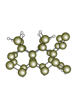
The Si(001) surface is represented by a repeated slab geometry. Each slab contains five Si atomic planes. The bottom layer Si atoms are passivated by hydrogen atoms. In addition, within the supercell, two consecutive rows of Si atoms extending along the [10] direction on the top layer are passivated with Hydrogen atoms (see Fig. 1). Consecutive slabs are separated by a vacuum space of 9 Å. The Si atoms on the top four layer of the slab and hydrogen atoms attached to top layer Si atoms are allowed to relax while Si atoms in the bottom layer of the slab and the passivating Hydrogen atoms are kept fixed to simulate the bulk like termination. The convergence with respect to the energy cutoff and the number of points for similar structures has been examined earlier ipb3 .
III results and discussions
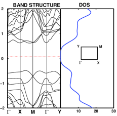
The lowest energy structure of the patterned dihydrogeneted Si(001) surface is shown in Fig. 1. The surface retains its unit periodicity along the y[10] direction. The unsaturated Si atoms on the surface (third row of Si atoms on the top layer in Fig. 1) forms a dangling bond wire extending along the y direction. Figure 2 shows the band structure (left panel) and the density of states (right panel) for the dangling bond wire. A wide band gap (1.3 eV) around the fermi level indicates that the surface is semiconducting in nature. The band gap is reflected in the density of states plot with vanishing density of states around the fermi level. This is in contrast to the metallic nature of dangling bond wire on monohydride Si(001): 21 surface.wat1 ; wat2 The reason behind the non-metallic nature of the dangling bond wire on the dihydrogeneted Si(001) is that the unit cell has two free electrons and they are fully accommodated in a single band below the fermi level.
Metal atoms are adsorbed on the surface shown in Fig. 1 to examine the possibility of the formation of a metallic nanowire supported on the Si substrate. Experiments have shown that the Al and Ga atoms can diffuse easily shen2 ; hash on the hydrogen terminated surface and therefore, the exposed Al, Ga and In atoms are expected to diffuse and nucleate around the Si dangling bonds on the surface. Thus it may be possible to form nanowire of metal atoms supported on the substrate. We are in search of a supported atomic wire that will be metallic in character. The adsorption of metals like Al, Ga and In is studied as a part of this search.

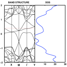
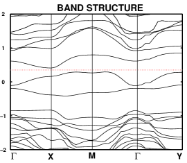
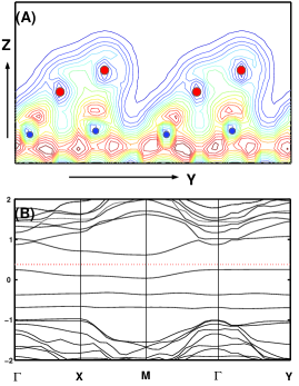
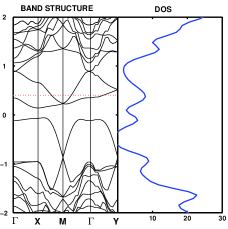
Here we consider the Al adsorption on the patterned dihydrogeneted Si(001) surface shown in Fig. 1. The surface offers various possible sites for the Al adsorption. Two different kinds of sites are denoted by S ( or ) and P ( or ) respectively as shown in Fig. 3. The sites vertically above the hydrogen free Si atoms (Si atoms with dangling bonds) are denoted as T ( or ). The configurations considered here are (one Al is placed on top Si atom marked as 1 and the other Al atom is placed on top of the Si atom marked as 2), (one Al is placed at site and the other one is placed at site) and (one Al is placed at site and the other is placed at site) respectively. For the configuration, the Al atoms are allowed to move along the z direction only, this configuration is found to be least favorable. The total energies of other configurations are calculated with respect to the total energy for the configuration. The and configurations are more favorable than the by 0.42 and 0.71 eV respectively. The configuration is interesting because the band structure and the density of states (see Fig. 4) for this structure indicate the metallic behavior of Al atomic wire extending along the y direction. On the other hand, the Al structure with the configuration shows non-metallic behavior (see a band gap around the fermi level in Fig. 5). For the configuration, each Al atom forms two bonds with two Si atoms (each Si-Al bond length is Å ) and the surface retains its unit periodicity along the y direction. Therefore, the single free electron of the Al atom in the unit cell is responsible for the partially filled bands crossings through the fermi level. Consequently the density of states increases around the fermi level and the atomic wire (with configuration) becomes metallic in character. For the configuration, we note that Al atoms make strong bonds with Si atoms (bond length Å while they fail to make a bond among themselves (distance between two Al atoms Å). In this configuration, the periodicity along y direction is doubled compared to that for the configuration. Two electrons from two Al atoms become non-itinerant in the unit cell, prefer to be occupied by a single band and hence the Al structure (with configuration) extending along the y direction becomes non-metallic. Similar to the zigzag Al chain considered earlier ipb2 ; ipb3 on the bare Si(001): 21, we also considered a zigzag Al chain configuration by displacing the Al atom at site by along the +ve x direction and the Al atom at site by along the -ve x direction. This zigzag chain configuration turned out to be unstable and readily reverted to the configuration.
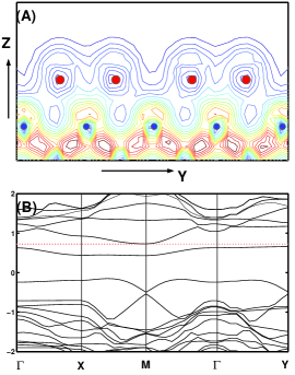
However, the most favorable configuration is the one where the Al atom at site is shifted along the positive y direction by 0.2 Å while that at the is shifted along the negative y direction by 1.6 Å to form a buckled Al dimer with a bond length of Å. The buckled Al dimers can be seen in charge density plot in the Fig. 6(A) where the large circles represent Al atoms while the small circles represent Si atoms (just below the Al wire). We will call this configuration as Al-dimer configuration and has a behavior akin to buckled Si dimer on Si (001). This is clear from the charge density plot in Fig. 6(A). The total energy of this configuration is -0.94 eV compared to the configuration, i.e., this Al-dimer configuration is favorable over configuration by 0.52 eV. This energy is gained mostly due to the optimization of Al-Si bonds and the superiority of Al-Al bond with respect to Al-Si bond. The nature of the Al wire extending along the y direction becomes non-metallic as can be seen from the band structure with an energy gap around the fermi level (see Fig. 6(B)). We therefore, conclude that the metallic Al nanowire ( corresponding to the configuration on the dihydrogeneted Si(001) can not be achieved in practice.
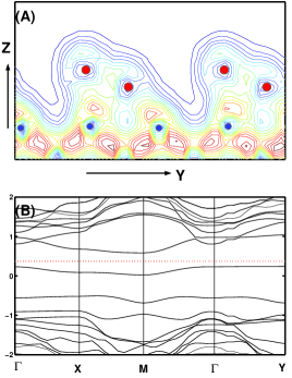
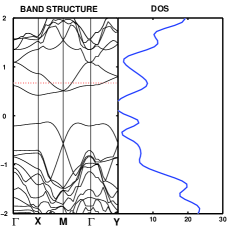
We nest consider the Ga adsorption on the same patterned dihydride Si(001). It is known that at some coverages, Ga behaves in a different way compared to Al ipb3 . The configuration is the least favorable one. However, unlike the case of Al, the configuration for Ga (total energy -0.41 eV compared to configuration) is slightly more favorable by 0.02 eV compared to the configuration. The Ga atomic wire with the configuration is metallic with a peak for density of states around the fermi level (see Fig. 7). However, the most stable configuration is very similar to that we found for Al. Two Ga atoms form buckled dimer as can be seen from the charge density plot in Fig. 8(A) (the large circles represent the Ga atoms and the small circles represent Si atoms just below the Ga atoms). This most favorable configuration is denoted as Ga-dimer configuration. The atomic wire made of buckled Ga dimers extending along the y direction is non-metallic in nature and this can be seen from the band structure plot in Fig. 8(B). Similar to the Al case, we therefore, conclude that stable metallic Ga wire can not be realized on patterned dihydrogenetd Si(001). We however, notice that the total energy difference between the Ga-dimer configuration and the configuration is 0.41 eV which is lower by 0.1 eV compared to that for the Al case. The reduction in the total energy difference between the and dimer configuration for Ga encourages us to study the In adsorption on the same patterned dihydrogented Si(001).
Unlike the case of Al and Ga the is the least favorable configuration for In. The total energy for this configuration compared to the configuration is +0.08 eV. The total energy for the configuration compared to the configuration is -0.20 eV. The In atomic wire with the configuration is metallic in character with large density of states around the fermi level and this can be seen from the band structure (left panel) and density of states (right panel) plot in Fig. 9. The most favorable configuration for In is a non-buckled In dimer as seen from the charge density plot in Fig. 10(A) where the In atoms (large circles in the figure) at and positions move towards each other by 0.3 Å to form a weak dimer. Consequently, the nanowire consisting of unbuckled weak In dimers becomes non-metallic (see the band structure in the Fig. 10 (B)). We note that the total energy for this configuration is -0.27 eV which is more favorable to the configuration only by 0.07 eV. At room temperature the thermal energy is expected to be sufficient to break these weak dimer bonds leading to metallic behavior of In wires on the dihydrogenetd Si(001). Here we add that there are situations where the experimentally observed structure corresponds to some local minimum energy structure. ipb3 ; bour Therefore, an experiment on this system is desirable to confirn if In atomic wire can be realized.
IV conclusion
First principle electronic structure calculations are performed to examine the possibility for the formation of stable metallic atomic wires on the dihydrogenetd Si(001). Adsorption of metals like Al, Ga and In are considered for this purpose. We found that the Al and Ga nanowire configurations with metallic character are strongly unstable towards the formation of buckled metal dimers leading to semiconducting behavior. However, the metallic In wire is weakly unstable because the total energy corresponding to the metallic wire configuration is very close to the most favorable non-metallic (weakly dimerised) configuration. The thermal energy may be able to break the weak bonds between In atoms and thus a metallic In wire may be realized on Si(001). Our results clearly indicates that as we go from Al to In via Ga, the metallic nanowire configuration approaches towards the most favorable one. We are hopeful that this work will encourage further experimental studies of In atomic wires on a patterned dihydrogeneted Si(001).
References
- (1) S. Hosoki, S. Hosaka, and T. Hasegawa, Appl. Surf. Sci. 60 643 (1992).
- (2) M. F. Crommie, C. P. Lutz, and D. M. Eigler, Science 262, 218 (1993).
- (3) T. -C. Shen, C. Wang, G. C. Abeln, J. R. Tucker, J. W. Lyding, Ph. Avouris, and R. E. Walkup, Science 268, 1590 (1995).
- (4) Advances in Scanning Probe Microscopy, eds. T. Sakurai and Y. Watanabe (Springer-Verlag, Berlin, 1989).
- (5) T. -C. Shen, C. Wang, and J. R. Tucker, Phys. Rev. Lett. 78, 1271 (1997).
- (6) Y. Wada, T. Uda, M. Lutwyche, S. Kondo, and S. Heike, J. Appl. Phys. 74, 7321 (1993).
- (7) D. S. Portal, E. Atracho, J. Junquera, P. Ordenjon, J. M. Soler, Phys. Rev. Lett. 83, 3884 (1999).
- (8) D. S. Portal, E. Atracho, J. Junquera, A. Garcia, and J. M. Soler, Surf. Sci, 482-485, 1261 (2001).
- (9) J. A. Torres, E. Tosatti, A. D. Coros, F. Ercolessi, J. J. Kohanoff, F. D. Di Tolla, and J. M. Soler, Surf. Sci. 426, L441 (1999).
- (10) M. Okamoto and K. Takayanagi, Phys. Rev. B 60, 7808 (1999).
- (11) H. Hakkinen, R. N. Barnett, U. Landman, J. Phys. Chem. B 103, 8814 (1999); H. Hakkinen, R. N. Barnett, A. G. Scherbakov, U. Landman, J. Phys. Chem B 104, 9063 (2000).
- (12) P. Sen, S. Ciraci, A. Budlum, and I. P. Batra, Phys. Rev. B 64, 195420 (2001).
- (13) P Sen, O. G lseren, T. Yildirim, I. P. Batra, and S. Ciraci, Phys. Rev. B 65, 235433 (2002).
- (14) I. P. Batra, T. Ciani, D. Boddupalli, and L. Soberano, Technical Preceedings of the 2003 Nanotechnology Conference and Trade Show, Shan Francisco, USA, 2, 206 (2003).
- (15) I. P. Batra, Phys. Rev. Lett. 63, 1704 (1989).
- (16) B. C. Gupta and I. P. Batra, Phys. Rev. B 69, 165322 (2004).
- (17) J. N. Crain, A. Kirakosian, K. N. Altmann, C. Bromberger, S. C. Erwin, J. L. McChesney, J. -L. Lin, and F. J. Himpsel, Phys. Rev. Lett. 90, 176805 (2003).
- (18) J. N. Crain, J. L. McChesney, Fan Zheng, M. C. Gallagher, P. C. Snijders, M. Bissen, C. Gundelach, S. C. Erwin, and F. J. Himpsel, Phys. Rev. B 69, 125401 (2004).
- (19) S. Watanabe, Y. Ono, T. Hashizume, and Y. Wada, Phys. Rev. B 54, R17308 (1996).
- (20) S. Watanabe, M. Ichimura, T. Onogi, and Y. Ono, Jap. J. Appl. Phys. 36, L929 (1997).
- (21) Adv. Phys. 42, 129 (1993).
- (22) F. S. Tautz and J. A. Schaefer, J. Appl. Phys. 84, 6636 (1998).
- (23) Y. J. Chabal and K. Raghavachari, Phys. Rev. Lett. 54, 1055 (1985).
- (24) J. J. Boland, Phys. Rev. Lett. 65, 3325 (1990).
- (25) J. J. Boland, Surf. Sci. 261, 17 (1992).
- (26) Y. J. Chabal and K. Raghavachari, Phys. Rev. Lett. 53, 282 (1984).
- (27) Y. Morita and H. Tokumoto, Appl. Phys. Lett. 67, 2654 (1995); Vac. Sci. Technol. A 14, 854 (1995).
- (28) G. Kresse and J. Hafner, Phys. Rev. B 47, R558 (1993); G. Kresse and J. Furtmuller, ibid. 54, 11169 (1996).
- (29) T. Hashizume, S. Heike, M. I. Lutwyche, S. Watanabe, K. Nakajima, T. Nishi, and Y Wada, Jap. J. Phys. 35, L1085 (1996).
- (30) B. Bourguignon, K. L. Cerleton, and S. R. Leone, Surf. Sci. 204, 455 (1988).