Effect of scattering and contacts on current and electrostatics in carbon nanotubes
Abstract
We computationally study the electrostatic potential profile and current carrying capacity of carbon nanotubes as a function of length and diameter. Our study is based on solving the non equilibrium Green’s function and Poisson equations self-consistently, including the effect of electron-phonon scattering. A transition from ballistic to diffusive regime of electron transport with increase of applied bias is manifested by qualitative changes in potential profiles, differential conductance and electric field in a nanotube. In the low bias ballistic limit, most of the applied voltage drop occurs near the contacts. In addition, the electric field at the tube center increases proportionally with diameter. In contrast, at high biases, most of the applied voltage drops across the nanotube, and the electric field at the tube center decreases with increase in diameter. We find that the differential conductance can increase or decrease with bias as a result of an interplay of nanotube length, diameter and a quality factor of the contacts. From an application view point, we find that the current carrying capacity of nanotubes increases with increase in diameter. Finally, we investigate the role of inner tubes in affecting the current carried by the outermost tube of a multiwalled nanotube.
pacs:
72.10.-d,73.23.Ad,73.63.Fg,73.63.Nm,73.63.RtI Introduction
Metallic carbon nanotubes are near ideal conductors of current frank-science-98 ; pablo-apl-99 ; poncharal-epjd-99 ; nygard-applphysa-99 ; kong-prl-01 . While a single nanotube can be used as an interconnect in molecular electronics, nanotube arrays have shown promise as more conventional interconnects in conjunction with silicon technology kreupl-microeleceng-02 ; ngo-eeetn-04 . A single nanotube has two modes that carry current at the Fermi energy, which yields a low bias conductance of and resistance of 6.5 . This corresponds to a current of 155 A at a bias of 1V. Noting that a nanotube diameter can be as small as 5 , it is easy to estimate that an array of metallic carbon nanotubes can carry current densities larger than . In fact, current densities approaching have been demonstrated pablo-apl-99 ; wei-apl-01 .
The diameter of both metallic and semiconducting nanotubes can vary from 5 to many tens of nanometers, with the electronic properties determined by the chiral angle. The bandgap of semiconducting nanotubes decreases inversely with diameter. As a result, a large diameter nanotube with a radius of 19 nm will have a bandgap of less than at room temperature, meaning that large diameter semiconducting nanotubes carry non negligible current. Further, electrical contact can be made to many shells of large diameter multiwalled carbon nanotubes. Reference pablo-apl-99 demonstrated a resistance of nearly 500 in a multiwalled sample, which corresponds to about twelve conducting shells. Therefore, both small and large diameter nanotubes are promising as interconnects. Experiments on small diameter carbon nanotubes show that the differential conductance decreases with applied bias, for voltages larger than 150 mV yao-prl-00 ; collins-prl-01 ; pablo-prl-02 . Reference yao-prl-00 showed that the conductance decreases with increase in bias was caused by reflection of electrons incident in crossing subbands due to scattering with zone boundary phonons. The non crossing subbands of small diameter nanotubes do not carry current due to their large band gap. In contrast, large diameter nanotubes experimentally show an increase in conductance with applied bias frank-science-98 ; poncharal-epjd-99 ; poncharal-jpcb-02 ; liang-apl-04 . Reference Anantram-prb-00 suggested that as the diameter increases, electrons may tunnel into non crossing subbands, thus causing an increase in differential conductance with applied bias. The main drawbacks of the calculation in reference Anantram-prb-00 was that the results depended on the assumed form of potential drop in metallic nanotubes and further, electron-phonon scattering was neglected. Recently, we performed self-consistent calculations svizhenko-cnt-ball , which showed a dramatic increase in differential conductance of large diameter nanotubes with bias, in the ballistic limit. In the current work, we present results for current flow and potential profile in metallic nanotubes from a more comprehensive model, which includes both charge self consistency and electron-phonon scattering. The potential and current-voltage characteristics are studied as a function of nanotube diameter and length. We are primarily interested in short ( 100 nm) rather than long nanotubes, where the physics is more interesting and technological applications are promising. The nature of the metallic contacts is also important. From an experimental view point the contact between a metal and a nanotube can either be an end-contact or side-contact. The end-contact corresponds to only the nanotube tip electronically interacting with the metal contact. In experiments, the end-contacts usually involves strong chemical modification of the nanotube at the metal-nanotube interface kong-prl-01 . Also, reference frank-science-98 found that end-contacts without sufficient chemical modification of the nanotube-metal interface have a large contact resistance. Due to the uncertainty of the contact bandstructure, modeling experimental end-contacts even remotely correct is difficult. The side-contacts correspond to coupling between metal and nanotube atoms over many unit cells of the nanotube, and can be thought of as a nanotube buried inside a metal. Most experimental configurations correspond to side-contacts frank-science-98 ; tans . An important feature of the side contact is that the coupling between atoms in the nanotube is much stronger than coupling between nanotube and metal atoms, which means that the bandstructure of the contacts is similar to that of the nanotube between the contacts. In the side-contact geometry, electrons are predominantly injected from the metal into the nanotube buried in metal and then transmitted to the nanotube region between contacts. In fact, as proof of such a process, scaling of conductance with contact area has been observed in the side-contacted geometry by references frank-science-98 ; tans . Modeling has also shown that the conductance in metallic zigzag nanotubes can be close to the theoretical maximum of , when there is sufficient overlap with the contact Anantram-apl-01 . In this work, we consider the metal-nanotube contact in both the limiting cases of side- and end-contacts.
The outline of the paper is as follows. In section II, we describe the formalism. The electrostatics at low bias is presented in section III.1, electrostatics at high bias and current-voltage characteristics are presented in section III.2. The role of inner shells in affecting the potential profile of a current carrying outer shell is described in section III.3. End-contacts that form both good and poor contacts are discussed in section III.4. We present our conclusions in section IV.
II Formalism
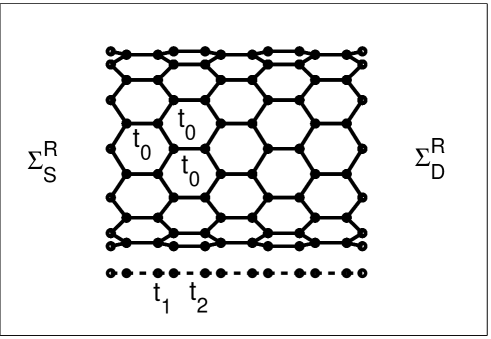
In this paper we consider only zigzag carbon nanotubes. The analysis for armchair nanotubes is similar. The general form of the Hamiltonian for electrons in a carbon nanotube can be written as:
| (1) |
The sum is taken over all rings in transport direction and all atoms located at in each ring.
We make the following common approximations: i) only nearest neighbors are included; each atom in an -coordinated carbon nanotube has three nearest neighbors, located 1.42 away; ii) the bandstructure consists of only -orbital, with the hopping parameter eV and the on-site potential . Such a tight-binding model is adequate to model transport properties in undeformed nanotubes. Within these approximations, only the following parameters are non zero:
| (2) | |||||
where . In zigzag nanotubes, the wave vector in the circumferential direction is quantized as , , creating eigenmodes in the energy spectrum. By doing a Fourier expansion of and in -space and using Eq. (2) we obtain a decoupled electron Hamiltonian in the eigenmode space:
| (3) | |||||
| (4) |
where
| (5) | |||||
The 1-D tight-binding Hamiltonian describes a chain with two sites per unit cell with on-site potential and hopping parameters and (Fig.1). For numerical solution, the spatial grid corresponds to the rings of the nanotube, separated by with a unit cell length of 2.13 , which is half the unit cell length of a zigzag nanotube. The number of spatial gridpoints is equal to the number of rings.
The subband dispersion relations are given by
| (6) |
Therefore, when , there are two subbands with zero bandgap the tube is metallic. In the rest of the paper we distinguish between metallic or crossing subbands ( and ) and semiconducting or non crossing subbands.
For each subband we solve a system of transport equations JAP :
| (7) | |||||
| (8) |
where . The self-energies and represent the effect of contacts and scattering.
The contacts are assumed to be reflectionless reservoirs maintained at equilibrium, i.e. they have well defined chemical potentials, equal to that of the metal leads: in the source and in the drain. Further, the nanotube and metal are assumed to have the same workfunction. The contact self-energies due to the source contact are found JAP using the surface Green’s function of the leads, which is the solution of the following system of equations:
| (9) |
where the indices and stand for the two sites of the unit cell, and are electron-phonon self-energies at the first two nodes near the source. The Green’s function for the drain are solved for in a similar way, by making the substitutions , and taking at the drain end. The expression for contact self-energies is then given by:
| (10) | |||||
where are the Fermi factors in the source and drain leads.
The electron-phonon scattering is treated within self-consistent Born approximation. The electron-phonon self-energies are due to elastic (acoustic phonon) and inelastic (optical and zone-boundary phonon) scattering:
| (11) |
| (12) | |||||
| (13) | |||||
| (14) | |||||
| (15) | |||||
| (16) |
The matrix elements squared due to particular scattering mechanisms are chosen so as to satisfy experimentally measured values of the mean free path . Reference park-nl-04 reported 1.6 and 10 nm for a tube with a diameter of 1.8 nm, corresponding to a (24,0) nanotube. Inelastic scattering is due to zone boundary and optical phonon modes with energies of 160 and 200 meV. Since, matrix elements squared scale inversely with the chirality index golgsman-prb-03 , one obtains for an nanotube
| (17) |
The decrease of a scattering rate in a single subband with the chirality index is saturated by the eventual increase of the intersubband scattering due to the larger number of subbands. Thus, with the increase of the diameter, the mean free path of a nanotube approaches that of graphite.
Electron charge and current density and at each node are found from the following equations:
| (18) | |||||
| (19) |
The lower limit of integration of Eq. (18) is determined by , where is a renormalization energy related to the real part of electron-phonon self-energy.
We model the electrostatics of the nanotube as a system of point charges between the two contacts located at and . The ”perfect contacts” are modeled as parallel semi-infinite three dimensional metal leads that are maintained at fixed source and drain potentials: for and for . So, while the self-energies due to contacts are identical to that of a semi-infinite nanotube, the role of electrostatics is included by image charges corresponding to a perfect metal. The electrostatic potential consists of a linear drop due to a uniform electric field created by the leads and the potential due to the charges on the tube and their images
| (20) |
with the Green’s function
| (21) | |||||
Here, is the radial projection of the vector between atom at ring and atom at ring . The summation is performed over all atoms at ring for an arbitrary value of . Maintaining the nanotube atoms buried in the metal at a fixed potential is close to reality because of the screening properties of 3D metals. Within a few atomic layers from the metal surface, the potential should have approached the bulk values. While the variation in potential in these few atomic layers of the 3D metal is not captured in our model, our conclusions on the nanotube electrostatics should not be significantly affected.
The calculations for one bias point involve two simultaneous iterative processes: Born iterations for electron-phonon self-energies [Eqs. (7-16)] and Poisson iterations of [Eqs. (7-20)] for the potential profile and charge distribution. Typically, Born iterations were performed before updating a potential profile using Eq. (20). The solution of Eqs. (7-8) employs a recursive algorithm JAP , which scales linearly with the number of nodes.
II.1 The importance of self-consistency and proper treatment of electron-phonon scattering
A major computational burden of the approach discussed above are the self-consistent procedure itself and also the Kramers-Krönig relation [Eq. (16)]. In order to take the integral in Eq. (16), at first, we have to solve Eqs. (7-15) over the whole band . Due to the presence of inelastic scattering, the energy grid has to be uniform. Typically, energy grid points are used in order to achieve a required precision in computing charge. At second, Eq. (16) requires multiplications for each subband, which makes it very time consuming. Such computational requirements pose a question on whether and what kind of sophistication is required in order to obtain an I-V characteristics. For a case of small diameter nanotubes, we note that a contribution to current by crossing subbands in metallic nanotubes under a moderate bias does not depend significantly on the potential profile. The reason is the density of states of crossing subbands is nearly constant around the Fermi energy and therefore the transmission is insensitive to the changes in the potential profile. It is also clear that the renormalization of subbands due to scattering affects only band edges, but does not influence the density of states of crossing subbands near the Fermi energy. These two facts, allow us to conclude that neither self-consistency nor Kramers-Krönig relation [Eq. (16)] is necessary to obtain an I-V characteristics in small diameter metallic nanotubes under a moderate bias. The criterium for this approximation is that bias is lower than the renormalized bandgap of the first non crossing subband , given by
Such an approximation, applicable e.g. to a nanotube under a bias smaller than V, while giving incorrect potential profiles would still result in a correct current with or without scattering.
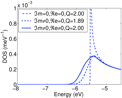
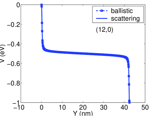
As will be seen later, in studying current through large diameter nanotubes it is important to take into account a current contribution by non crossing subbands. Tunneling current by non crossing subbands has a lower threshold bias [Eq. (II.1)] and depends exponentially on the slope of the potential near the edges of the tube. Therefore, a self-consistent solution for the shape of tunneling barrier is must for large diameter nanotubes at all biases. This, in turn, necessitates the exact knowledge of electron charge and density of states. We now discuss how much the real part of electron-phonon retarded self-energy and thus the renormalization of the density of states affects the potential profile. In previous studies TED was set to zero, which naturally alleviates computational requirements. In Fig.2 we show the density of states of crossing subbands versus energy in a nanotube under a zero bias. The Poisson iterations were switched off and the potential . Three curves represent different approximations to electron transport: a ballistic case, when both real and imaginary parts of electron-phonon self-energies are set to zero (dash-dotted line), a scattering case, when only imaginary part is taken into account (dashed line), and a scattering case, when both imaginary and real part are non zero (solid line). For scattering cases, transport equations were iterated for long enough to achieve convergence of electron-phonon self-energies, i.e. self-consistent Born approximation is satisfied. The area under the ballistic curve is equal to which is twice the charge per subband. The important consequence of taking into account only imaginary part of retarded self-energy is that the area decreases, resulting in loss of electron charge. When both real and imaginary parts are taken into account, electron charge is recovered due to the shift of the subband bottom. The loss of charge when the real part is neglected results in a completely incorrect potential profile when solving transport equations self-consistently with Poisson equation [Eq. (20)]. In Fig.3 we show potential profiles with and without a real part of electron-phonon self-energy when both Born and Poisson iterations have converged. The applied voltage drops symmetrically across the nanotube, when the scattering is treated properly (solid line). When the real part is neglected, the profile shows a severe down shift due to a missing electron charge (dashed line). Such incorrect potential profile will result in large error in current due to non crossing subbands in large diameter nanotubes. Another source of error is an overestimated bandgap [Eq. (II.1)] and higher threshold for the onset of current due to non crossing subbands. In this work, all our self-consistent calculations included Eq. (16) for the real part of electron-phonon self-energy.
III Results
III.1 Electrostatics at low bias
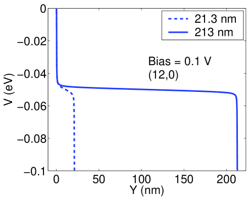
The mean free path due to scattering with acoustic phonons is in the range of a micron yao-prl-00 ; park-nl-04 . At low biases, i.e. biases lower than inelastic phonon energy, electron-phonon scattering does not play a significant role in determining the potential profile for wires of moderate length (less than few hundreds of nanometer). The potential profiles for (12,0) nanotubes of lengths 21.3 and 213 nm are shown in Fig. 4. The edges of the nanotube near the contact rapidly screen the applied bias / electric field. The potential drop is divided unequally between different parts of the nanotube, with 90% of the applied bias falling within 1 nm from the edges for both lengths.
While the density of states (DOS) per unit length of metallic nanotubes is independent of diameter, the DOS per atom is inversely proportional to the diameter:
| (23) |
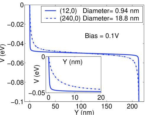
where is the number of atoms in a ring of an (N,0) nanotube. As a result, we find that the screening of metallic nanotubes degrades with diameter. The potential drop for two nanotubes with diameters of 0.94 nm [(12,0) nanotube] and 18.8 nm [(240,0) nanotube] are shown in Fig. 5. Clearly, screening is poorer in the larger diameter nanotube. In fact, while the potential drops by 45 mV in a distance of 1 nm from the edge for the (12,0) nanotube, the potential drop is only 17 mV for the (240,0) nanotube. The inset of Fig. 5 shows a substantially larger electric field away from the edges of the large diameter nanotube.
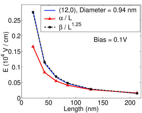
The electric field at the center of the nanotube as a function of length is shown in Fig. 6 for the tube with a diameter of 0.94 nm. We find that for all diameters, the electric field decreases more rapidly than , where is the length of the nanotube. The exact power law however depends on the diameter. If the computed electric field versus length is fit to , the exponent increases with increase in chirality. The value of increases from 1.25 to 1.75 as the diameter increases from 0.94 to 18.85 nm. Similarly, electric field versus diameter can be fit to , where is in the range between 0 and 1.
III.2 Electrostatics at high bias and current-voltage characteristics
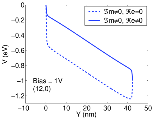
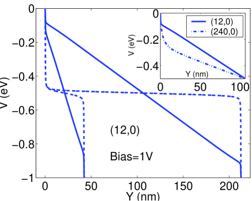
At biases larger than 150 mV, the main scattering mechanism in defect free carbon nanotubes is electron-phonon interaction. Kane et al.yao-prl-00 found that emission of zone boundary and optical phonons are the dominant scattering mechanisms. The potential profiles at high bias for 42.6 and 213 nm long (12,0) nanotubes are shown in Fig. 7. Due to the increased resistivity of the tube the potential profile drops almost uniformly across the entire nanotube, which is qualitatively different compared to the low bias (and no scattering) results of Fig. 4. The potential drop at the edges of the nanotube accounts for only 30% of the applied bias. Because a bias drops in the bulk of the tube at the expense of the edges, the potential drop at the edges also decreases with increase of nanotube length, falling to 15% for the longer nanotube. Due to the diameter dependence of the scattering rates, the (12,0) tube is 20 times more resistive than (240,0), with mean free path of 5 nm for (12,0) versus 100 nm for (240,0). As a result, contrary to the low bias case, the potential profiles for larger diameter tubes show a larger voltage drop at the edges (inset of Fig. 7).
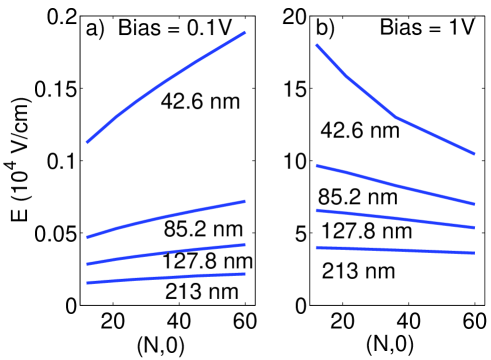
A major consequence of different potential profiles of large and small diameter nanotubes at low and high bias is the electric field at the nanotube center: the electric field is smaller in the small diameter nanotube in the ballistic limit but the onset of electron-phonon scattering at high bias makes the electric field larger. This interesting reversal in electric field, demonstrated in Fig. 8 is rationalized by noting that the potential drop in the (12,0) nanotube has become almost linear because the mean free path is much smaller than nanotube length, unlike in the (240,0) nanotube.
So far electrostatics of nanotubes under applied bias was discussed. We now compare the potential profiles in the ballistic limit and with scattering, in a non zero electric field but at equilibrium. We choose an external electric field corresponding to a V bias but the Fermi levels of the source and drain contacts are set to V. The electrostatic potential profiles in the two cases are almost identical as shown in Fig.9 in sharp contrast to the non equilibrium case. The reason is, at equilibrium, following the Thomas-Fermi model, the potential profile should depend only on DOS at Fermi energy, which is unaffected by electron-phonon scattering.
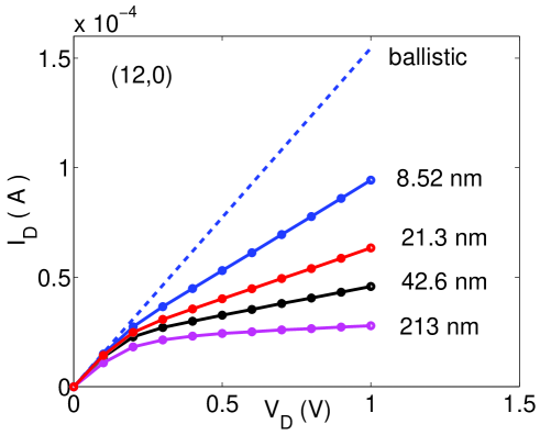
We now discuss the current voltage characteristics of small and large diameter nanotubes. For the (12,0) nanotube, only two crossing subbands contribute to transport. The ballistic current increases linearly with applied bias and the differential conductance is . Scattering by inelastic phonons causes current saturation and the decrease of the differential conductance (Fig. 10). As the length of the nanotube is increased, so is the number of scattering events. The family of current - voltage characteristics show the transition from ballistic to diffusive transport regime. The current saturation at the value of 25 A for the longest tube agrees well with experimental data.
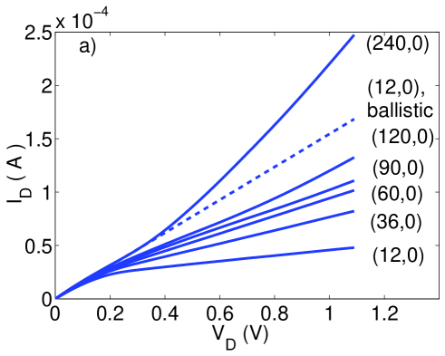
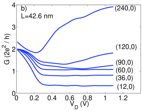
Current and differential conductance versus bias for a nm nanotubes and a wide range of diameters are shown in Fig.11. At low bias, phonon scattering is weak, so the current and conductance are still close to the ballistic limit. The saturation of current corresponds to the onset of inelastic phonon scattering and to the decrease of conductance at high bias. Differential conductance for small and moderate diameter nanotubes ( 12, 36 and 60) is qualitatively similar because of the same number of conducting modes. Quantitatively, the conductance increases with diameter due to decreasing scattering rates. This transition from low to high bias regime is also present in large diameter nanotubes ( 90, 120 and 240).
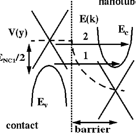
We note that current increases with diameter. In the ballistic limit, the self-consistently calculated current of (240,0) nanotube at 1V is 310 A and the differential conductance is almost . When scattering is included the current is decreased to 218.3 A which is much larger than the current carried by a (12,0) nanotube of the same length, which is 45.7 A. In addition, the differential conductance versus bias exhibits a qualitative change in shape. It is bell-shaped for small diameter nanotubes and transforms to U-shaped for large diameter nanotubes. As explained in svizhenko-cnt-ball , the increase of differential conductance with bias occurs due to injection of electrons from contacts into the low energy non crossing subbands. A schematics of Zener tunneling process is shown in Fig.12: when the bias becomes larger than twice the bandgap of the lowest non crossing subband, electrons can tunnel from valence band states () in the source to the conduction band states () in the middle of the tube (the channel) and also from valence band states in the channel to the conduction band states in the drain. The lowest non crossing subbands () in (90,0), (120,0) and (240,0) in the ballistic limit have bandgaps 331, 249 and 125 meV respectively and start to contribute to current at biases of twice these values. We note that the above picture is based on the assumption that the applied voltage drops symmetrically across the nanotube. In the case when one contact is much more resistive than the other and the applied voltage drops completely at one of the edges, the threshold for Zener tunneling is reduced, starting at biases equal to rather than . Additionally, if the contacts are metallic (and not perfect nanotube contacts), then the threshold bias for tunneling into non crossing subbands will be further reduced by a factor of 2, an issue that will be discussed in section III.4. In addition to Zener tunneling between states with the same quantum number , scattering also induces a phonon assisted tunneling from bonding states of non crossing subbands to crossing subbands. Although these processes require intersubband scattering, the threshold bias is twice as low.
Another important feature of differential conductance occurs at zero bias in (240,0) nanotube (Fig.11). The zero bias conductance of (240,0) nanotube is larger than because the non crossing subbands are partially filled and contribute to current: the first non crossing subband opens at an energy of 2.4 from the band center. This contribution is a simple intraband transport, determined by the population of the conduction band in the source and the valence band in the drain, but rather insensitive to the details of the potential profile. At slightly higher biases the non crossing subbands contribution to current saturates to a constant value and the contribution to differential conductance decreases to zero, while the total conductance decreases to .
Increasing the length of a nanotube eventually makes the nanotube length larger than the mean free path. The current carried by a 213 nm long (240,0) nanotube is now 86.6 A at 1V. Note that the differential conductance of a long nanotube, shown in the inset of Fig.13, has changed to bell-shaped, in contrast to the short nanotube case presented in Fig.11. This is because when the nanotube length is many times the mean free path, the potential drop in the nanotube bulk becomes more linear and as a result the barrier width (Fig.12) for tunneling into non crossing subbands increases. The, non crossing subbands then do not carry significant current. Over all, the voltage drop at the edges is a crucial factor determining the current contribution due to non crossing subbands. It is directly related to the height and width of the barrier for tunneling into non crossing subbands (Fig.12), which depends on the scattering rate, nanotube length and screening capability.
In the rest of the paper we discuss the role of electrostatic coupling to inner shells of a large diameter nanotube and the role of contacts. Specifically, we will see that both issues lead to increased tunneling into non crossing subbands because they lead to a decrease in barrier thickness.
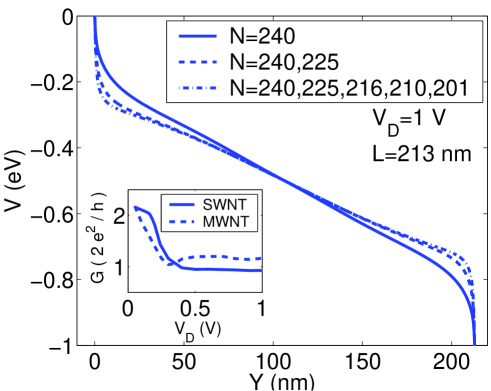
III.3 Electrostatic gating due to inner shells
In multiwalled nanotubes (MWNT) current flows only through the outermost shell as the inner shells are not electronically coupled to the metal leads liang-apl-04 , and inter shell hopping is negligible bourlon-prl-04 . Here, we are interested in the role of electrostatic coupling between the inner and outer shells, in affecting the potential profile and current carried by the outer shell. We find that the inner shells effectively decrease the barrier width for tunneling into non crossing subbands by providing additional screening. Fig.13 shows the potential profile in the outermost (240,0) shell. The inner shells are chosen to be metallic nanotubes with chirality indices 225, 216, 210 and 201, such that a separation between the walls is roughly Å. Even when just one metallic shell (225,0) is added, the barrier width for tunneling into the first non crossing subband decreases dramatically from 2.97 to 0.97 nm. Adding more shells further reduces the barrier width by smaller amounts, and the effect saturates. The differential conductance with the inner shells is qualitatively different as shown for the 213 nm long (240,0) nanotube in the inset of Fig.13. We find that the differential conductance at higher biases is larger but does not show an increase with bias, when inner shells are included.
III.4 Influence of contact quality
We have so far assumed that the contacts are perfect, i.e. made of semi-infinite carbon nanotube leads. As mentioned in the introduction, this physically corresponds to carbon nanotubes weakly coupled to the metal in which they are buried. So, injection of electrons into the carbon nanotube lying between the contacts occurs from the carbon nanotube buried in the metal. As a result of this, injection into non crossing subbands from the contact cannot occur at E=0. Note that selection rules don’t permit injection of electrons from the crossing subband of the nanotube contact into non crossing subbands between the contacts. In this section, we relax this condition and consider injection from the source contact into all nanotube subbands. The drain contact continues to be a nanotube contact. To accomplish this in a phenomenological manner, we model the contact self energies in Eq. (10) as,
| (24) |
where is the original hopping parameter in Eq. (10), is called the quality factor of the contacts, and is the density of states of the contact which is chosen to be close to that of gold, . The self energy in Eq. (24) permits injection into the first non crossing subband at a bias of rather than the with nanotube contacts.
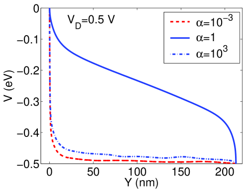
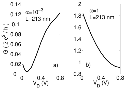
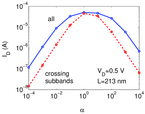
We now present results for the potential profiles with good () and poor ( and ) contacts in Fig.14. Note that the terminology of poor and good contact is a relative to the intrinsic resistance of the nanotube that arises due to electron-phonon scattering. For , the potential profile of a (240,0) nanotube of length 213 nm is more or less symmetric and qualitatively similar to the perfect contact results presented in Fig.13. For and , the electrostatic potential drops predominantly at the source-end due to the large source-end contact resistance. The large potential drop and hence extremely thin barrier in the source-end will facilitate tunneling into the non crossing subbands for poor contact. As mentioned before, the asymmetry of the potential profile further reduces the threshold for Zener tunneling to biases of . The difference between the potential profiles for good and poor contacts has a profound influence on the shape of the differential conductance versus bias as shown in Fig.15. For good contacts, the 213 nm long nanotube shows a decreasing conductance with bias, in agreement with the perfect contact case. In contrast to this, for poor contacts, the differential conductance increases with bias. This increase with bias is a direct consequence of the potential profile shown by the dashed line in Fig.14, which facilitates significant injection into non crossing subbands. To see more directly that the non crossing subbands are important in carrying current in long nanotubes with poor contacts, we calculate the current carried at a drain bias of 0.5 V as a function of the quality factor of the contacts, with only crossing subbands and with all subbands. For good contacts, the current with only crossing subbands is very close to the current with all subbands (Fig.16). But for poor contacts, the current with all subbands is significantly higher than the current with only crossing subbands. For example, when , the current with all subbands is nearly an order of magnitude larger than with only crossing subbands. From Fig.16 one can also see that the U-shaped differential conductance curve versus bias should be observed in a wide range of except a small region near , where non crossing subbands do not carry a significant current.
IV Conclusion
We have studied transport in nanotubes of varying diameters and length, with electron-phonon scattering included. We find that charge self-consistency and the proper treatment of subband renormalization due to scattering are crucial in determining the correct current-voltage characteristics in large diameter metallic nanotubes. In the small bias ballistic limit, while the applied bias drops predominantly at the nanotube-contact interfaces, screening is incomplete at the tube center. Further, screening improves with decrease in nanotube diameter due to the increased density of states per atom near the Fermi energy. At biases larger than 150 mV, electron-phonon scattering becomes important and the electrostatic potential drops primarily in the bulk of the nanotube rather than at nanotube-contact interfaces. However, as the mean free path for electron-phonon scattering increases with increase in nanotube diameter, the potential drop in the bulk of the nanotube is larger for small diameter nanotubes. As a result, the electric field at the nanotube center increases with increase in diameter at small biases, and decreases with increase in diameter at high biases. This interesting reversal in electric field versus diameter is computationally seen for nanotube lengths from 42 to 213 nm. Over all, we find that larger diameter nanotubes are capable of carrying more current because of increase in mean free path with increase in diameter and lower bias threshold for injection into non crossing subbands. For small diameter nanotubes of length 42 nm, we find that the differential conductance versus bias is bell-shaped, with the largest value at zero bias. The reason for the smaller differential conductance at larger bias is reflection of electrons due to inelastic phonon scattering and availability of only crossing subbands for charge transport. In contrast, large diameter nanotubes of the same length show an increase in differential conductance with increase in bias due to injection into non crossing subbands and larger mean free paths. At a nanotube length (213 nm) longer than the mean free path, we find that the differential conductance for large diameter nanotubes transitions to a bell-shaped curve similar to the small diameter case, when coupling to contacts is good (small contact resistance). We have also modeled the role of inner shells in affecting the potential profile of the outer shell of a multiwalled nanotube. Here, we find that the inner shells cause a change in the electrostatic potential profile of the outer shell so as to make the potential drop sharper at the nanotube-contact interfaces. Our computational study has shown that the potential drop and differential conductance in metallic nanotubes is determined by an interesting interplay of diameter, mean free path, nature of contacts and bias threshold for tunneling into non crossing subbands. Finally, the most important result of this paper is that a quality of contacts is a primary factor in determining the shape of the differential conductance versus bias in large diameter nanotubes. When the resistance at the nanotube-contact interface is larger than the intrinsic resistance of the nanotube, there is a large potential drop at the interface. This potential drop facilitates considerable tunneling into non crossing subbands and as result the differential conductance of the 213 nm long (240,0) nanotube with poor contact increases with bias, in contrast to the case with good contacts. This finding gives a possible explanation to the increase in differential conductance with bias seen in the recent experiment of reference liang-apl-04 .
Acknowledgements.
The calculations were performed at the facilities of NASA Advanced Supercomputing Division. We would like to thank Avik Ghosh for discussions on the density of states of gold.References
- (1) S. Frank, P. Poncharal, Z. L. Wang and W. A. de Heer, Science 280, 1744 (1998)
- (2) P. Poncharal, S. Frank, Z. L. Wang and W. A. de Heer, Eur. Phys. J. D 9, 77 (1999)
- (3) P. J. de Pablo, E. Graugnard, B. Walsh, R. P. Andres, S. Datta and R. Reifenberger, Appl. Phys. Lett. 74, 323 (1999)
- (4) J. Nygard, D. H. Cobden, M. Bockrath, P. L. McEuen and P. E. Lindelof, Appl. Phys. A 69, 297-304 (1999)
- (5) J. Kong, E. Yenilmez, T. W. Tombler, W. Kim, H. Dai, R. B. Laughlin, L. Liu, C. S. Jayanthi, and S. Y. Wu, Phys. Rev. Lett. 87, 106801 (2001)
- (6) F. Kreupl, A. P. Graham, G. S. Duesberg, W. Steinhogl, M. Liebau, E. Unger and W. Honlein, Microelectron. Eng. 64, 399-408 (2002)
- (7) Q. Ngo, D. Petranovic, S. Krishnan, A. M. Cassell, Q. Ye, J. Li, M. Meyyappan and C. Y. Yang, IEEE Trans. Nanotech. 3, 311 (2004)
- (8) B. Q. Wei, R. Vajtai and P. M. Ajayan, Appl. Phys. Lett. 79, 1172-1174 (2001)
- (9) Z. Yao, C. L. Kane and C. Dekker, Phys. Rev. Lett., 84, 2941 (2000)
- (10) P. G. Collins, M. Hersam, M. Arnold, R.Martel and Ph. Avouris, Phys. Rev. Lett. 86, 3128-3131 (2001)
- (11) P. J. de Pablo, C. Gomez-Navarro, J. Colchero, P. A. Serena, J. Gomez-Herrero and A. M. Baro, Phys. Rev. Lett., 88, 36804 (2002)
- (12) P. Poncharal, C. Berger, Y. Yi, Z. L. Wang and W. A. de Heer, J. Phys. Chem. B 106, 12104 (2002)
- (13) Y. X. Liang, Q. H. Li and T. H. Wang, Appl. Phys. Lett. 84, 3379-3381 (2004)
- (14) M. P. Anantram, Phys. Rev. B 62, 4837 (2000)
- (15) A. Svizhenko, M. P. Anantram, T.R. Govindan, submitted to IEEE Trans. on Nano Tech., (2005)
- (16) S.J. Tans, M. Devoret, H. Dai, A. Thess, R.E. Smalley, L.J. Geerligs, and C. Dekker, Nature, v. 386, p. 474 (1997)
- (17) M. P. Anantram, Appl. Phys. Lett., v. 78, p. 2055 (2001)
- (18) A. Svizhenko, M. P. Anantram, T.R. Govindan, R. Venugopal, J. Appl. Phys., 91, 2343 (2002)
- (19) J. Park, S. Rosenblatt, Y. Yaish, V. Sazonova, H. Ustunel, S. Braig, T. A. Arias, P. W. Brouwer and P. L. McEuen, Nano Lett. 4, 517 (2004)
- (20) G. Pennington and N. Goldsman, electrons is semiconducting carbon nanotubes Phys. Rev. B 68, 045426 (2003)
- (21) A. Svizhenko, M. P. Anantram, IEEE Ttrans. Electron. Dev., 50, 1459 (2003)
- (22) B. Bourlon, C. Miko, L. Forro, D. C. Glattli, A. Bachtold, Phys. Rev. Lett., 93, 176806 (2004)