Quasi-ballistic, nonequilibrium electron distribution in inhomogeneous semiconductor structures
Abstract
We report on a study of quasi-ballistic transport in deep submicron, inhomogeneous semiconductor structures, focusing on the analysis of signatures found in the full nonequilibrium electron distribution. We perform self-consistent numerical calculations of the Poisson-Boltzmann equations for a model GaAs structure and realistic, energy-dependent scattering. We show that, in general, the electron distribution displays significant, temperature dependent broadening and pronounced structure in the high-velocity tail of the distribution. The observed characteristics have a strong spatial dependence, related to the energy-dependence of the scattering, and the large inhomogeneous electric field variations in these systems. We show that in this quasi-ballistic regime, the high-velocity tail structure is due to pure ballistic transport, whereas the strong broadening is due to electron scattering within the channel, and at the source(drain) interfaces.
pacs:
73.23.Ad, 72.15.Lh, 72.20.Ht, 73.40.KpAs the downscaling of semiconductor devices has reached well into the deep submicrometer regime, the nonequilibrium nature of the carrier dynamics has become exceedingly important. In these systems, channel lengths comparable to the electron mean free path are possible at room temperature, and thus, ballistic and hot electron effects are expected to strongly influence the transport properties of modern devices. Although numerous studies of hot electron and ballistic transport have been performed,ravaioliSST98 there have been very few works on the microscopic carrier dynamics. It is, e.g., not clear how the details of the scattering at the channel interfaces, as well as within the channel, affect the ballistic nature of the transport, what the microscopic signatures of quasi-ballistic transport are, and how these issues are responsible for limiting the current in these systems.lundstromIEEE02 ; svizhenkoIEEE03
A comprehensive microscopic analysis of these issues requires the study of the
electron distribution function, which is a challenging task, both
experimentally
and theoretically, due to the strongly nonequilibrium nature of the problem.
There have been a few recent theoretical studies of ballistic MOSFETs
lundstromIEEE02 ; rhewSSE02 in
which the electron distribution was obtained by solution of the
Boltzmann Transport Equation (BTE) in the collisionless limit. In this
pure ballistic limit, according to the models, the electron distribution
within the channel is composed of near-equilibrium electron distributions
in the contacts,
and thus, due to the inhomogeneous self-consistent field, only displays
an asymmetric, pronounced high-velocity peak, corresponding to ballistic
electrons. In recent experimental studies on the other hand,experiments
the
electron distribution in submicron, inhomogeneous III-V systems was
measured using Raman spectroscopy, and was shown to display strongly
broadened velocity distributions and interesting high-velocity tail
structure. It is clear that in realistic room-temperature devices, the
electron scattering rate is finite and thus, a full solution of the BTE,
including scattering is required. Such an analysis was in fact already
initiated by Baranger and Wilkins.baranger
These authors solved the BTE self-consistently with the Poisson equation
for GaAs structures, and found significantly
out-of-equilibrium electron distributions in the channel region, and
in particular, a high-velocity peak corresponding to ballistic
electrons. However, the physical mechanisms of the strong broadening
and the details of the electron distribution characteristics were not
clearly resolved. In addition, the scattering introduced in the BTE
was structureless, while the distribution function in inhomogeneous
systems is strongly energy-dependent.
In this paper we present a numerical analysis of the nonequilibrium
electron distribution in submicron, inhomogeneous semiconductor
structures. We show that the electron distribution function has a
highly nonequilibrium form, is significantly broadened, and displays
interesting structure in the high-velocity tail. In addition, the
observed features are spatially dependent and very sensitive to the
inhomogeneous electric field, temperature and detailed characteristics
of the scattering, where we find that an energy-dependent scattering
process strongly affects the details of the electron distribution. In
addition to providing insight to the general
quasi-ballistic transport
characteristics in the electron distribution of submicron structures,
we believe that our results are relevant for the recently observed
nonequilibrium velocity distributions observed in the recent
experiments.
Our study is based on numerical analyses in which we explictly calculate the 1D, steady-state electron velocity distribution function, , through a model GaAs structure.parameters We consider a nondegenerate system and use a numerical, self-consistent approach based on the coupled Poisson-Boltzmann equations, which enables us to capture essential nonequilibrium and inhomogeneous transport phenomena.csontosJCE04 Scattering is treated within the relaxation-time approximation, using realistic, energy-dependent scattering rates corresponding to polar-optical phonon (POP) scattering, which is the dominating scattering mechanism in GaAs at room temperature.scattering The POP scattering rate is given bynag
| (1) | |||||
where , is the high-frequency dielectric constant, is the static dielectric constant, is the optical phonon energy and is the phonon occupation number. In Eq. (1) the first term corresponds to POP absorption and the second to POP emission, which only occurs when .
In Fig. 1 we show the electron potential energy, electric field and distribution function at K, and V, for a 200 nm long lightly doped ( cm-3) GaAs slab sandwiched between two highly doped ( cm-3) long contacts. In order to highlight the effects of inhomogeneities and scattering while keeping the nature of the scattering structureless, we first use constant scattering times in our calculations (in Fig. 1, s), and subsequently compare these results with realistic energy-dependent scattering times. For comparison, the potential energy and electric field at are plotted in Fig. 1(a) (dashed lines). Several direct observations can be made from the electrostatics depicted in Fig. 1(a). A potential barrier is formed in the region due to the inhomogeneous doping profile that gives rise to the diffusion of electrons from the highly doped into the lightly doped region. Second, as a result, a strong electric field on the order of 10 kV/cm is formed within the device, even in the absence of an external field. Third, as a bias voltage is applied, a large portion of the voltage drop occurs over the submicron region, giving rise to a strongly inhomogeneous field distribution, in contrast to the contact regions, where the field in comparison is very low and constant.
In Fig. 1(b), the calculated normalized electron distribution function, , where is the thermal velocity, is shown at different spatial points along the sample for the V case. At m, the electrons injected from the source display a shifted MB distribution. This is expected throughout the highly-doped contact regions, where the field is constant and low ( 0.1 kV/cm) and thus, the distribution function can be described by the linear response solution to the homogeneous BTE, . At m, corresponding to the top of the potential barrier, the distribution is asymmetric, showing a suppression of electrons in the tail of the distribution. This is caused by the asymmetric potential barrier, which prevents left-moving electrons () to reach . Deep in the region, for , the electron distribution displays a strong spatial dependence as well as significant broadening. To better understand the overall spatial dependence of the distribution function, Fig. 1(c) shows the contour plot of , around the interesting region. It is clear that the electron distribution in the region displays a distinct peak that is rapidly shifted toward higher velocities for increasing . This is a signature of ballistic transport and occurs due to the rapid and large (compared to ) potential energy drop baranger ; lundstromIEEE02 ; rhewSSE02 and corresponding strong inhomogeneous electric field. In addition to the ballistic peak, for increasing , the electron distribution is broadened and a low-velocity contribution gradually builds up until the distribution is dominated by a low-velocity peak, see point in Fig. 1(b) and the spatial dependence in Fig. 1(c). The origin of this broadening is two-fold: The thermionically injected electrons at , with , are gradually thermalized at a rate as they cross the channel, thus gradually “depopulating” the high-velocity peak
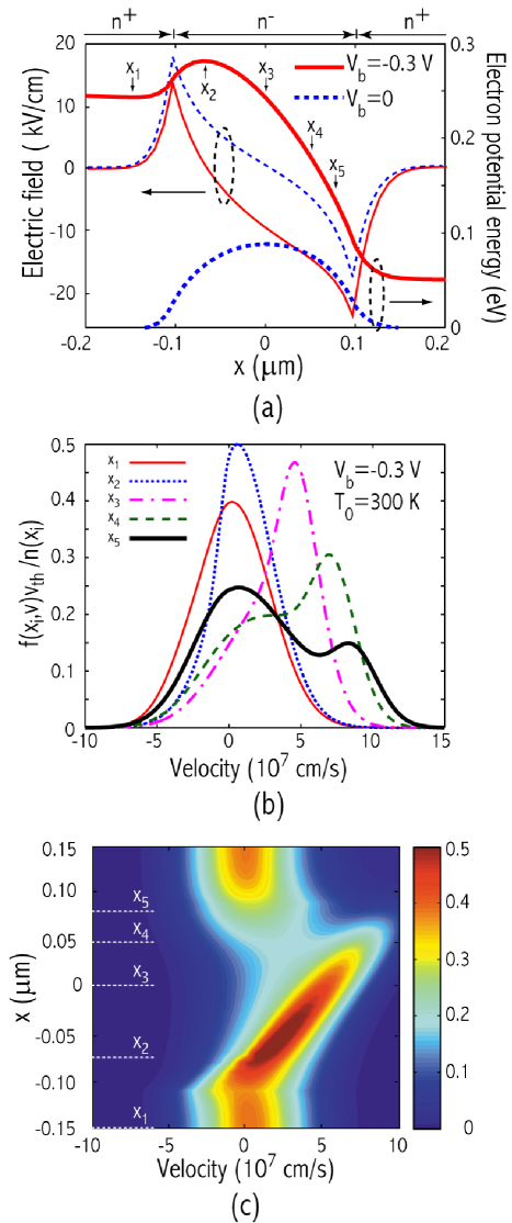
corresponding to ballistic electrons. Second, electrons backscattered at the channel-drain interface, as well as injected electrons with from a near-equilibrium distribution in the drain, penetrate the channel with negative velocities, contributing to the negative and low-velocity end of the electron distribution. These electrons are scattered at a rate , but also experience scattering at the steep potential energy barrier close to the source. Hence, close to the source and deep in the region, the distribution is dominated by the ballistic peak corresponding to the source-injected ballistic electrons [see Fig. 1(b)]. Close to the drain, however, where the effective potential barrier is lower, the drain-injected and reflected electrons dominate the distribution and obscure the ballistic peak.
The spatial dependence of the electron velocity distribution is strongly influenced by the characteristics of the external and built-in fields, mobility, scattering mechanisms and temperature. In Fig. 2(a), (b) we show the distribution function calculated for the constant scattering times s and s, for the same structure and system parameters studied in Fig. 1 (with s). While energy-independent, these scattering times correpond to realistic mobilities of GaAs. For the short scattering time, s, the ballistic peak structure seen in Fig. 1(c) is significantly less pronounced and the average velocity of the electrons is strongly reduced. The latter observation is a natural consequence of the increase of the scattering rate. However, in addition, the fraction of the potential drop that occurs over the channel region also decreases with an increase in the scattering rate (not shown here) and hence, due to the decreased effective potential barrier, the drain-injected and reflected electrons penetrate deep into the channel. Therefore, the resulting distribution, although strongly out-of-equilibrium, does not display distinct ballistic features, but becomes broadened, asymmetric and shifted. For s [Fig. 2(b)], the opposite effects are observed: A very distinct ballistic peak dominates the distribution function deep into the region close to the drain, and less broadening is observed. This is due to an increase in the electron velocity given by the decreased scattering rate, and an increase in the effective potential barrier seen by electrons with coming from the drain.
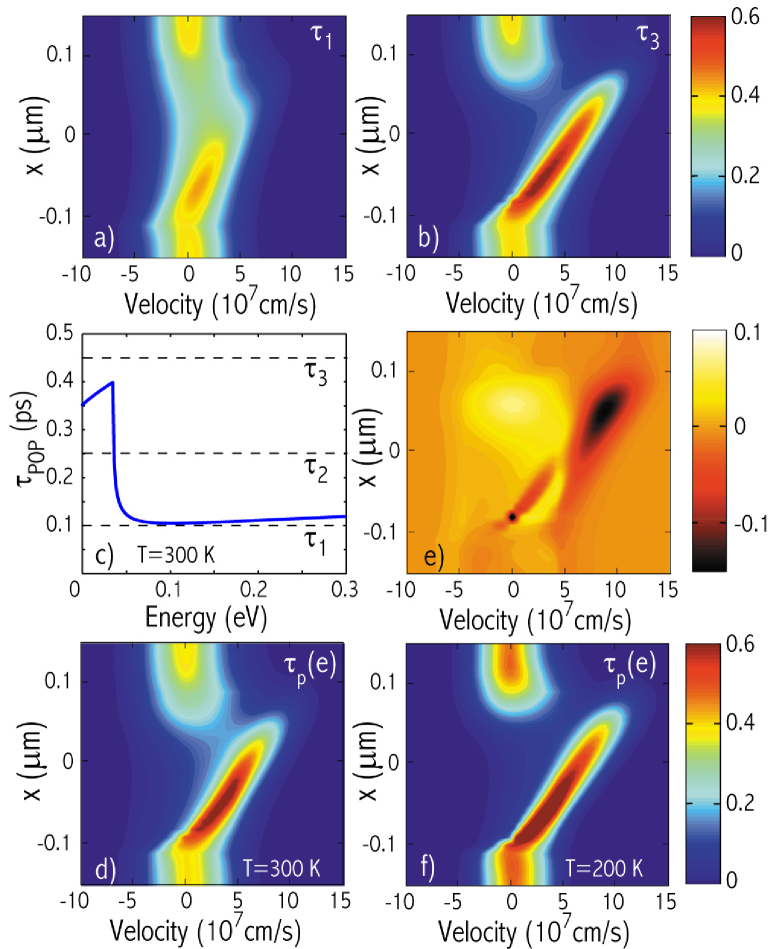
In realistic systems, the scattering and relaxation processes can have a strong energy-dependence and thus, it is interesting to consider the effects of an energy-dependent scattering rate on the nonequilibrium distribution function. In Fig. 2(c) the energy-dependent POP scattering time , calculated from Eq. (1) at K, is shown. For clarity, in the figure, we have also indicated the values of the constant scattering times used in the calculations shown in Figs. 2(a), (b) and 1(c). Below the threshold for POP emission, the scattering time is in the range s, whereas above the threshold, the scattering time has a relatively weak dependence on energy (in this particular energy interval) and is close to s. The corresponding electron distribution function, calculated at K is shown in Fig. 2(d). Strong signatures of quasi-ballistic transport are seen, i.e., formation of a ballistic peak that evolves toward higher velocities, similarly to the calculations performed with the constant, energy-independent scattering times, and significant broadening and low-velocity contributions due to the scattering processes discussed above. The details of the distribution function and its spatial dependence are, however, different. In Fig. 2(e), the difference between the normalized functions [ and are the electron densities corresponding to the two calculated distribution functions] is shown. The observed difference can be explained as follows: Electrons with velocities below cm/s, which corresponds to a kinetic energy comparable to the threshold for POP emission [Fig. 2(c)], have a large mean free path and behave ballistically, as concluded by the results shown by the calculations for shown in Fig. 2(b). For electrons with higher kinetic energies on the other hand the scattering rate is higher and thus the electrons relax toward lower energies at an increasing rate. However, the picture is more complicated, since the detailed energy-dependence of the scattering effectively also changes the characteristics of the inhomogeneous field due to the charge redistribution caused by the scattering.
Finally, we briefly discuss the effects of temperature, which is the parameter that, next to the applied electric field, is most easily tuned in experiments. In Fig. 2(f) we show the electron distribution calculated at K. Below the threshold for POP emission, the calculated scattering time (not shown here) is in the range s, whereas above threshold, the scattering time has weak energy dependence and is s. As anticipated from the above discussion, the main effects of lowering the temperature and, thus, increasing of the phonon scattering time, are: higher average velocities, larger spatial extension of the ballistic peak, narrowing of the ballistic peak in the n- region as well as the diffusive peaks in the source/drain, and suppression of the drain-injected electron contribution to the electron distribution in the channel region, due to an increase in the effective potential barrier.
In summary, we have studied the electron distribution in inhomogeneous, deep submicron semiconductor structures by self-consistent calculations of the semiclassical BTE. We have shown that the electron distribution in general is strongly out-of-equilibrium, significantly broadened and displays pronounced structure in the high-velocity tail. These characteristics of quasi-ballistic transport are very sensitive to the energy-dependent scattering in the channel and at the source(drain) interface, as well as the strongly inhomogeneous electric field. Our results are similar to recent experimental observations.
Note added after submission: An interesting study of quasiballistic
transport in nanoscale semiconductor structures with focus on the scattering
and the mathematical nature of the BTE at the top of the potential energy barrier
at the source-channel interface has been published very recently
by Sano.sanoPRL04 ; sanoAPL04 We note that
although the calculations were done for completely different material (Si)
and system parameters, the features of the distribution shown in Fig. 3
of Ref. sanoAPL04, are similar to the features of the distributions
calculated here, and are due to the mechanisms discussed in our paper.
This work was supported by the Indiana 21st Century Research and Technology Fund.
References
- (1) See, e.g., U. Ravaioli, Semicond. Sci. Technol. 13, 1 (1998), and references therein.
- (2) M. Lundstrom, and Z. Ren, IEEE Trans. Electron Devices 49, 133 (2002).
- (3) A. Svizhenko, and M. P. Anantram, IEEE Trans. Electron Devices 50, 1459 (2003).
- (4) J.-H. Rhew, Z. Ren, and M. S. Lundstrom, Solid State Electronics 46, 1899 (2002).
- (5) E. D. Grann et al., Phys. Rev. B 51, 1631 (1995); E. D. Grann et al., Phys. Rev. B 53, 9838 (1996); K. T. Tsen et al., Appl. Phys. Lett. 69, 3575 (1996); W. Liang et al., Appl. Phys. Lett. 82, 1413 (2003); W. Liang et al., Appl. Phys. Lett. 84, 3681 (2004).
- (6) H. U. Baranger, and J. W. Wilkins, Phys. Rev. B 36, 1487 (1987); H. U. Baranger, and J. W. Wilkins, Phys. Rev. B 30, 7349 (1984).
- (7) GaAs material parameters: , , , eV.
- (8) D. Csontos and S. E. Ulloa, (to be published in J. Comp. Electronics). Also available at arXiv.org, cond-mat/0411499.
- (9) scattering, while possibly comparable to POP scattering in the regions, is much weaker in the channel region due to the low doping ( cm-3).
- (10) B. R. Nag, Theory of electrical transport in semiconductors (Pergamon Press, Oxford, 1972).
- (11) N. Sano, Phys. Rev. Lett. 93, 246803 (2004).
- (12) N. Sano, Appl. Phys. Lett. 85, 4208 (2004).