Topological defects in the edge state structure in a bilayer electron system.
Abstract
We experimentally demonstrate, for the first time, formation of point-like topological defects in the edge state structure in the quantum Hall effect regime. By using of a selective population technique, we investigate equilibration processes between the edge states in bilayer electron structures with a high tunnelling rate between layers. Unexpected flattening of the curves in perpendicular magnetic field at a specific filling factor combination and the recovery of the conventional nonlinear characteristics in tilted fields give a strong evidence for the existence of topological defects.
pacs:
73.40.Qv 71.30.+hSince its introduction by Halperin halperin , the concept of the edge states (ES) was found to be useful in describing transport phenomena in two-dimentional (2D) systems for both sharp buttiker and smooth shklovsky edge potential profile. ES are arising in a quantizing magnetic field at the intersections of the Fermi level with distinct Landau levels, which are bent up by the edge potential.
Much attention was paid to substantiate the ES picture experimentally by investigating electron transport along ES, as well as between them (for a review, see Ref. haug, ). Different imaging techniques shashkin ; klitzing were used to demonstrate the existence of compressible and incompressible strips of the electron liquid at the sample edge, which is widely accepted nowadays.
However, there is another class of phenomena in ES that has not been investigated yet. It is the formation of so-called topological defects, which have been predicted to occur, e.g., when two ES with different spins locally switch their positions and thus cross each other at several (at least two) points demsley ; bauer . Possible mechanism for such a crossover was proposed theoretically for a non-equilibrium occupation of spin-split ES, when the chemical-potential difference is of the order of the spin splitting bauer . This situation can not be achieved in usual experiments performed in the Hall-bar geometry mueller . In recent experiments in quasi-Corbino geometry alida ; rdiff with direct biasing of the ES, no sign of ES crossing was observed, even when the ES imbalances exceeded the cyclotron gap relax . This may be due to the fact that even at the crossing points, the electron spin flips, which are necessary for the inter-ES scattering, can be strongly suppressed mueller .
More pronounced features may be expected in the transport properties of bilayer systems, where not only spin, but also isospin, related to the layer index zheng , is involved. The energies of the isospin states can be tuned in situ by application of a suitable gate voltage, which, as we will show below, gives direct control over the presence of the topological defects.
Here, we experimentally study topological defects (namely, the edge state crossings) in a bilayer electron system. We use a selective population technique to investigate equilibration processes between different edge states. By adjusting the gate voltage and the magnetic field, we force the bilayer system to be in different isospin states in the gated and ungated regions, that leads to a crossing of the ES, which we detect in the transport characteristics.

Measurements are performed in a quasi-Corbino sample geometry, in which a top gate of special shape is used to independently contact ES and bring them into interaction over a distance which is much smaller than the equilibration length alida . In Fig. 1 (a), only the interaction region of the sample is shown. Voltage V , applied between contacts that are connected to the inner and outer ES (not shown in Fig. 1), produces an energy shift between them. This allows to directly investigate the charge transfer between ES in the interaction region (gate-gap) at imbalances even higher than the spectral gaps.
In gated bilayer systems, such as the one with quasi-Corbino geometry used here, the gate bias does not only influence the lateral, but also the vertical distribution of charge. At zero gate voltage, the bilayer systems studied here are slightly imbalanced (i.e. they have different electron concentrations in two parts of the well). A negative top-gate bias increases this initial imbalance, see Fig. 1 (b). The electric field mostly affects the electron density in the top (closest to the gate) layer of the well, which will deplete at some bias (the bilayer onset voltage). At lower gate voltages, only the back part of the well is filled, so that the electron system becomes a single-layer. Thus, even for a sample where the edge states in the gate gap originate from the bilayer spectrum, the channels under the gate may originate from either a bi- or a single-layer spectrum. By using samples with different it is therefore possible to realize different regimes under the gate, even at the same filling factor. For a single-layer system in a quantizing magnetic field, the energy spectrum is the usual Landau ladder of energy levels. In the bilayer regime, the situation is more sophisticated dqw ; tilt ; davies ; japan . In imbalanced bilayer systems, the electrons belong to a particular electron sheet, which makes it necessary to introduce a new quantum number: the isospin, or layer index, equal to for top/bottom layer, correspondingly). In sufficiently high magnetic fields (corresponding to low filling factors 1 and 2), and/or in balanced electron system, the electrons have non-zero wave functions in both layers and, consequently, are in a mixed isospin state. The energy spectrum is then a single Landau ladder with an additional energy gap: the symmetric-antisymmetric splitting .
Another way to couple both layers is through application of an in-plane magnetic field component. Not only does it increase the Zeeman splitting with respect to other energy scales, but it also forces common subband formation tilt even at high filling factors .
In the present paper we investigate the samples at filling factor in the gate-gap. In perpendicular magnetic field, ES originate from two independent Landau ladders (see Fig. 2 a). The separation between the two outer spin-split ES and the single inner one is given by the difference of the subband energies of the two electron layers.
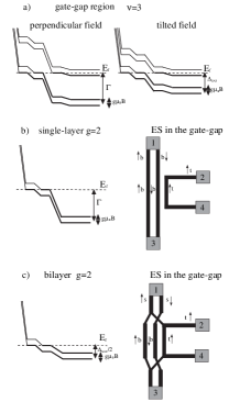
Let us first consider the case when the electron system under the gate is in a single-layer regime for filling factor g = 2. Two spin-split energy levels in the bottom electron layer form two ES, which are directly connected to the two outer spin-split ES in the gate-gap, because the same spin and isospin indexes are the same (see Fig. 2 b). Applying a bias voltage to the ohmic contacts 1 and 2 in Fig. 2 produces an energy shift of the two outer ES in the gate-gap with respect to the inner one. Positive voltage flattens the potential relief between the ES alida ; rdiff because of . Significant current starts to flow only after complete flattening of the subband bottom, i.e. at , so this branch of the curve should contain a clear-defined threshold. Applying a negative voltage produces only a tunnel current between ES, leading to a strongly non-linear branch.
Let us now turn to the case where the gated region is in the bilayer regime at . Then the one to- one correspondence between the edge states in the ungated and gated parts is no longer possible and a new ES topology will develop, as shown in Fig. 2 (c), right. Under the gate, two energy levels are filled. They both correspond to the lowest (symmetric) subband and are separated by the spin gap, see Fig. 2 (c), left. Electrons in the corresponding ES belong to both electron layers simultaneously. Roughly speaking, there is probability to find an electron in either layer. When a charge is injected into the gate-gap region, both spin and isospin should be conserved. Isospin conservation means that approximately half of electrons are injected into the top electron layer and the others are injected into the bottom layer. Taking into account the spin conservation, we conclude that the electrons from the outer ES under the gate will be injected into both the outermost and the innermost ES in the gate-gap, so they will share the same chemical potential. Thus, the ES can cross each other in the corners of the gate-gap, as sketched in Fig. 2 (c), right. Two ES with the same spin in the gate-gap will be full-equilibrated, leading to linear curve.
The described picture can easily be destroyed by an in-plane magnetic field component. As mentioned above, in tilted magnetic fields the states in the gate-gap region will also be delocalized between both layers. As shown in Fig. 2 (a), right, two spin-split ES will originate from the lowest, (symmetric) quantum well state, while the third ES will be associated with the antisymmetric state, separated by . Because the two outermost edge states now have the same isospin in both gated and ungated regions of the sample, the ES topology will resemble the one shown in Fig. 2 (b), left. Therefore, there will be no ES crossing and the I-V curves should become strongly non-linear again, as in the single-layer case. The height of the step on positive branch of I-V curve will now be given by .
From the picture above described we expect that ES crossing can be realized in samples where the gated and ungated parts are in a different isospin configuration. The equilibration caused by the crossing should lead to a linear trace. This linear ’s in normal magnetic fields and the recovery of the conventional nonlinear characteristics in tilted fields are the key features of the topological defects in bilayer systems.
Our samples are from two different wafers, A and B, grown by molecular beam epitaxy on semi-insulating GaAs substrate. They are GaAs/AlGaAs quantum wells of different width and shape. For wafer A, active layers form a 760 Å wide parabolic quantum well, whereas for wafer B, a 300 Å wide quantum well is of rectangular form. In the center of each well, a 3 monolayer thick AlxGa1-xAs () sheet is grown, which serves as a tunnel barrier. The symmetrically doped wells are capped by 600 Å AlxGa1-xAs () and GaAs layers. Both structures, A and B, contain 2DEG of similar electron concentration (about cm-2) and mobility. They are slightly imbalanced (i.e., have unequal electron concentrations in two parts of the well).
The samples are patterned in a quasi-Corbino geometry alida . Ohmic contacts are made to both electron layers simultaneously. In the experiment we study the characteristics of the gate-gap region at the temperature of 30 mK in magnetic fields up to 14 T. Tilting the sample plane with respect to the magnetic field allows us to introduce an in-plane field component to affect the energy spectrum of the bilayers. The electron concentration in the ungated region was obtained from usual magnetoresistance measurements. Also, magnetocapacitance measurements were performed to determine the energy spectrum under the gate dqw .
The onset voltage , at which the system becomes single-layer, is very different for both samples: V for the wafer A and V for the wafer B. Therefore, at the filling factor combination which we are interested in here, the samples are in different isospin configurations. For sample A, is obtained at , so that the sample is in a bilayer regime. Sample B, on the other hand, is single-layer at (). Both samples are in an equivalent isospin state at the filling factor combination (, resulting in a single layer under the gate), which can be used as a reference.
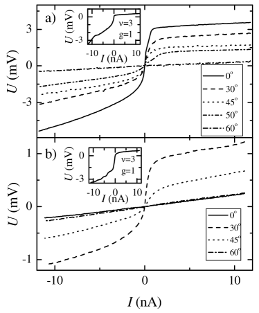
In Fig. 3, curves are presented for both types of the samples, in normal and tilted magnetic fields. For the sample that is single-layer at (Fig 3 (a)), the curves are strongly non-linear. They have a well-defined threshold at positive voltages ( meV in a perpendicular field), above which a current starts to flow. The value of the threshold corresponds to the subband splitting.
In contrast, the sample with bilayer (A-type, Fig 3 (b)) has a fully linear curve in perpendicular magnetic fields. This demonstrates the absence of a gap between the inner and outer edge states, in agreement with the ES picture discussed above (Fig. 2 (c), right). Tilting the sample, while keeping the normal field component constant, causes the curve to become strongly non-linear. This is in agreement with the prediction that the in-plane field component will remove the topological defects and re-establish a gap structure (see Fig. 2 (a), right).
Further increase of the tilt angle flattens curves, similarly for both sample types. It is important, that even at the highest tilt angle , ’s for both samples are slightly non-linear, while in a perpendicular field, the curve is fully linear for the sample of type A.
The conclusion that the different behavior of the two samples shown in Fig. 3 is related to the different isospin configuration is further supported by measuring the -characteristics at the filling factor combination . In this case, both samples are in the same isospin configuration, and the curves are qualitatively similar for both samples in perpendicular (see inserts to Fig. 3), as well as in tilted fields (not shown here). They are non-linear and asymmetric, with a small positive threshold voltage given by the spin gap.
As mentioned above, the linear curve of sample A for the filling factor combination in a perpendicular magnetic field indicates full equilibration between the inner and any (or both) of two outer ES in the gate-gap region. Figure 2 (c), right, suggests that the innermost ES will only interact with the outermost ES (but not the middle one) if the spin conservation is assumed. We find that the experimental slope exactly coincides with one obtained from Buttiker’s calculation rdiff if the equilibration in the gate-gap is established between two of the ES involved. This allows us to draw the following conclusions: (i) because the gate-gap width (2 m) is much smaller than the characteristic equilibration lengths in transport between the ES (of the order of 100m, see Refs. haug, ; mueller, ), a defect must be present which very efficiently couples different ES; (ii) this defect only couples ES with the same spin in the gate-gap; (iii) the equilibration by the defect is destroyed by an in-plane field component. These experimental findings, combined together, give strong evidence that the defect is not an impurity of some kind, but indeed a topological defect induced by the different isospin configurations in the gated and ungated regions of the sample.
We wish to thank Dr. A.A. Shashkin and Yu.A. Melnikov for help during the experiment. We also thanks Greg Snider for the Poisson-Schrodinger solver. We gratefully acknowledge financial support by the RFBR, RAS, the Programme ”The State Support of Leading Scientific Schools”, Deutsche Forschungsgemeinschaft, and SPP ”Quantum Hall Systems”, under grant LO 705/1-2. E.V.D. acknowledges support by Russian Science Support Foundation.
References
- (1) B. I. Halperin, Phys. Rev. B 25, 2185 (1982).
- (2) M. Büttiker, Phys. Rev. B 38, 9375 (1988).
- (3) D. B. Chklovskii, B. I. Shklovskii, and L. I. Glazman, Phys. Rev. B 46, 4026 (1992).
- (4) R.J. Haug, Semicond. Sci. Technol. 8, 131 (1993).
- (5) A. A. Shashkin, A. J. Kent, J. R. Owers-Bradley, A. J. Cross, P. Hawker, M. Henini, Phys. Rev. Lett. 79, 5114 (1997).
- (6) Y. Y. Wei, J. Weis, K. von Klitzing, K. Eberl, Phys. Rev. Lett. 81, 1674 (1998).
- (7) Jed Dempsey, B. Y. Gelfand, and B. I. Halperin Phys. Rev. Lett. 70, 3639 3642 (1993); B. Y. Gelfand and B. I. Halperin Phys. Rev. B 49, 1862 1866 (1994).
- (8) Lex Rijkels and Gerrit E. W. Bauer, Phys. Rev. B 50, 8629 (1994).
- (9) G. Müller, D. Weiss, A. V. Khaetskii, K. von Klitzing, S. Koch, H. Nickel, W. Schlapp, and R. Lösch, Phys. Rev. B 45, 3932 (1992).
- (10) A. Würtz, R. Wildfeuer, A. Lorke, E. V. Deviatov, and V. T. Dolgopolov, Phys. Rev. B 65, 075303 (2002).
- (11) E. V. Deviatov, V. T. Dolgopolov, A. Wurtz, JETP Lett. 79, p. 618 (2004).
- (12) E. V. Deviatov, A. Wurtz, A. Lorke, M. Yu. Melnikov, V. T. Dolgopolov, D. Reuter, A. D. Wieck, Phys. Rev. B 69, 115330 (2004).
- (13) L. Zheng, R.J. Radtke, and S. Das Sarma, Phys. Rev. Lett. 78, 2453 (1997).
- (14) V. T. Dolgopolov, A. A. Shashkin, E. V. Deviatov, F. Hastreiter, M. Hartung, A. Wixforth, K. L. Campman, and A. C. Gossard Phys. Rev. B 59, 13235 (1999).
- (15) Deviatov E.V., Khrapai V.S., Shashkin A.A., V. T. Dolgopolov, F. Hastreiter, A. Wixforth, K. L. Campman, A. C. Gossard, JETP Lett 71 496 (2000).
- (16) A. Sawada, Z.F. Ezawa, H. Ohno, Y. Horikoshi, Y. Ohno, S. Kishimoto, F. Matsukara, M. Yasumoto, and A. Urayama, Phys. Rev. Lett. 80, 4534 (1998)
- (17) A.G. Davies, C.H.W. Barnes, K.R. Zolleis, J.T. Nicholls, M.Y. Simmons, and D.A. Ritchie, Phys. Rev. B 54, R17331 (1996).