Abstract
Recent advances in atomic and nano-scale growth and characterization techniques have led to the production of modern magnetic materials and magneto-devices which reveal a range of new fascinating phenomena. The modeling of these is a tough theoretical challenging since one has to describe accurately both electronic structure of the constituent materials, and their transport properties. In this paper I review recent advances in modeling spin-transport at the atomic scale using first-principles methods, focusing both on the methodological aspects and on the applications. The review, which is designed as tutorial for students at postgraduate level, is structured in six main sections: 1) Introduction, 2) General concepts in spin-transport, 3) Transport Theory: Linear Response, 4) Transport Theory: Non-equilibrium Transport, 5) Results, 6) Conclusion. In addition an overview of the computational codes available to date is also included.
Ab-initio methods for spin-transport at the nanoscale level
Stefano Sanvito
Department of Physics, Trinity College Dublin, Ireland
email: sanvitos@tcd.ie
1. Introduction
According to a recent issue of “Physics Today”, the traditional study of magnetism and magnetic materials has an image of “musty physics laboratories peopled by old codgers with iron filings under their nails” [1]. However over the last few years new advances in atomic- and nano-scale growth and characterization techniques have led to the production of modern magnetic materials and magneto-devices which reveal a range of new fascinating phenomena.
This new renaissance in the study of magnetism has been initiated by the discovery of the Giant Magnetoresistance (GMR) effect in magnetic multilayers [2, 3]. GMR is the drastic change in the electrical resistance of a multilayer formed by alternating magnetic and non-magnetic materials when a magnetic field is applied. In absence of an external magnetic field the exchange coupling between adjacent magnetic layers through the non-magnetic ones [4] aligns the magnetization vectors antiparallel to each other. Then when a magnetic field strong enough to overcome the antiferromagnetic coupling is applied, all the magnetization vectors align along the field direction. The new “parallel” configuration presents an electrical resistance considerably smaller than that of the antiparallel: this change in resistance is the GMR.
The main reason why GMR was such an important milestone is that not only the interplay between transport and magnetism was demonstrated, but also that the spin degree of freedom could be engineered and exploited in a controlled way. In other words GMR established that the longly neglected electron spin could be used in the similar way that the electron charge in an electronic device. In the remarkable short time of about a decade, GMR evolved from an academic curiosity to a major commercial product. Today GMR-based read/write heads for magnetic data storage devices (hard-drives) are in every computers with a huge impact over a multi-billion dollar industry, and magnetic random access memory (MRAM) based on metallic elements will soon impact another multi-billion industry.
Most recently, in particular after the advent of magnetic semiconductors [5, 6], a new level of control of the spin-dynamics has been achieved. Very long spin lifetime [7] and coherence [8] in semiconductors, spin coherence transport across interfaces [9], manipulation of both electronic and nuclear spins over fast time scales [10], have been all already demonstrated. These phenomena, that collectively take the name of “spintronics” or “spin electronics” [11, 12, 13] open a new avenue to the next generation of electronic devices where the spin of an electron can be used both for logic and memory purposes. Quoting a recent review of the field “the advantages of these new devices would be nonvolatility, increased data processing speed, decreased electrical power consumption, and increased integration densities compared with conventional semiconductor devices” [11]. The ultimate target is to go beyond ordinary binary logic and use the spin entanglement for new quantum computing strategies [14]. This will probably require the control of the spin dynamics on a single spin scale, a remote task that will merge spintronics with the rapidly evolving field of molecular electronics [15].
Interestingly, it is worth noting that most of the proposed spintronics implementations/ applications to date simply translate well-known concepts of conventional electronics to spin systems. The typical devices are mainly made by molecular beam epitaxy growth, and lithographic techniques; a bottom-up approach to spintronics devices has been only poorly explored. This is an area where the convergence with molecular electronics may bring important new breakthroughs. The idea of molecular electronics is to use molecular systems for electronic applications. This is indeed possible, and conventional electronic devices including, molecular transistors [16], negative differential resistance [17], and rectifiers [18] have been demonstrated at the molecular level. However in all these “conventional” molecular electronics applications the electron spin is neglected.
Therefore it starts to be natural asking whether the fields of spin- and molecular electronics can be integrated. This basically means asking: “how can we inject, manipulate and detect spins at the atomic and molecular level?” It is worth noting that in addition to the fact that a molecular self-assembly approach can substitute expensive growing/processing technology with low-cost chemical methods, spintronics in low dimensional systems can offer genuine advantages over bulk metals and semiconductors. In fact, molecular systems are mainly made from light, non-magnetic atoms, and the conventional mechanisms for spin de-coherence (spin-orbit coupling, scattering to paramagnetic impurities) are strongly suppressed. Therefore the spin coherence time is expected to be several orders of magnitude larger in molecules than in semiconductors. Strong indications on possibility of integrating the two fields come from a few recent pioneering experiments demonstrating spin injection [19] and magnetic proximity [20] into carbon nanotubes, molecular GMR [21], huge GMR in ballistic point contacts [22, 23, 24], spin injection into long polymeric materials [25] and spin coherent transport through organic molecules [26].
It is therefore clear that a deep understanding of the spin-dynamics and of the spin transport at the molecular and atomic scale is fundamental for further advances in both spin- and molecular- electronics. This is an area where we expect a large convergence from Physics, Chemistry, Materials Science, Electronical Engineering and in prospective Biology. The small lengths scale and the complexity of some of the systems studied put severe requirements to a quantitative theory.
Theory has been at the forefront of the spintronics “revolution” since the early days. For instance spin transport into magnetic multilayers has been very successfully modeled by the widely known Valet-Fert theory [27]. This is based on the Boltzmann’s equations solved in the relaxation time approximation, which reduce to a resistor network model in the limit of long spin-flip length. The main aspect of this approach is that the details of the electronic structure of the constituent materials can be neglected in favor of some averaged quantities such as the resistivity. Such methods are based on the idea that the scattering length scale is considerably shorter than the typical size of the entire device. Clearly the scheme breaks down when we consider spin transport at the molecular and atomic scale. In this situation individual scattering events may be responsible for the whole resistance of a device and an accurate description is needed in order to make quantitative predictions. In particular a theory of spin-transport will be predictive if it comprises the following two ingredients:
-
1.
An accurate electronic structure calculation method which relies weakly on external parameters
-
2.
A transport method able to describe charging effects
At present there are several approaches to both electronic structures and transport methods, but very few algorithms that efficiently include both. The purpose of this paper is to present an organic review of spin transport methods at the nanoscale, in particular of approaches which are based on parameter-free ab initio electronic structure calculations. I will incrementally add details to the description with the idea to make the paper accessible to non-experts to the field. The prototypical device that I will consider is the spin-valve. This is a trilayer structure with a first magnetic layer used as spin-polarizer, a non-magnetic spacer and a second magnetic layer used as analyzer. I will consider as non-magnetic part either metals, or insulators or molecules.
Since the field is rather large, this review does not pretend to be exhaustive, but only to provide a didactic introduction to the fascinating world of the theory of both spin- and molecular-electronics. In doing that I will overlook several important aspects such as semiconductors spintronics, theory of optical spin excitation and femtosecond laser spectroscopy, and non-elastic spin transport in molecules, for which I remand to the appropriate literature.
The paper is structured with a section describing the main ideas behind spin-transport at the nanoscale with reference to recent experimental advances, followed by a tutorial presentation of a transport algorithm based on the non-equilibrium Green’s function approach. Here I will make a link with other approach and review the computer codes available to date. Finally I will review a selected number of problems where ab initio spin-transport theory has led to important new developments.
2. General concepts in spin-transport
2.1 Length scales
The modeling of spin-transport at the nanoscale using ab initio methods brings together different aspect of materials science such as magnetism, transport and electronic materials. Each one of those has some characteristic length scales, and it is crucial to understand how these relate to each other. This of course allows us to identify the limit of validity of our theoretical description. Moreover it is important to compare these length scales with the range of applicability of modern quantum mechanical methods. Often we cannot describe a system just because it is “too big” for our computational capabilities. It is therefore crucial to have some understanding of the level of precision we want to achieve. The best method is the one offering the best tradeoff between accuracy and computational overheads for the problem under investigation. A summary of the length scales relevant for spin-transport in presented in figure 1.
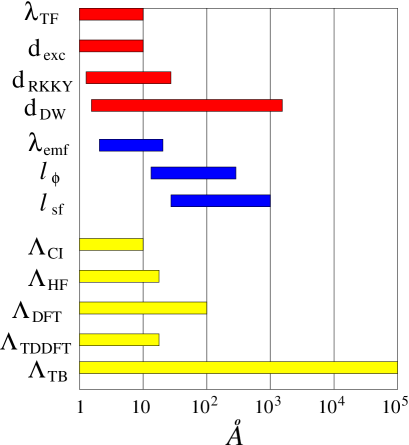
2.1.1 Electronic and Magnetic Lengths
These are length scales connected with the range of the electrostatic and magnetic interactions.
Screening Length
When a charge is introduced in a neutral material (say a metal) this produces a perturbation in the existing electronic potential. In the absence of any screening effect this will add a coulombic-like potential to the existing potential generated by both electrons and ions. However when conduction electrons are present they will respond to the perturbation of their potential by effectively screening the potential of the additional charge. Following the elementary Thomas-Fermi theory [28, 29, 30, 31] the “screened” potential is of the form:
| (2.1) |
where is the screening length. For a free electron gas this can be written as
| (2.2) |
where is the electron charge, the density of state (DOS) at the Fermi level and the vacuum permittivity. Given the large density of state at , for typical transition metals is of the order of the lattice parameters 1-10 Å. This means that the charge density of a transition metal is unchanged at about 10 Å from an electrostatic perturbation such as a free surface or an impurity.
Exchange
The coupling between spins in a magnetic material is governed by the exchange interaction, which ultimately is related to the exchange integral. This depends on the overlap between electronic orbitals and therefore is rather short range, usually of the order of the lattice parameter. Therefore the typical length scale for the exchange interaction is of the same order than the screening length. In addition in atomic scale junctions most of the atoms which are relevant for the transport reside close to free surfaces or form small clusters. These may present features at a length scale comparable with the lattice constant that are rather different from that of the bulk. For this reason specific calculations are needed for specific atomic arrangements and the extrapolation of the magnetic properties at the nanoscale from that of the bulk is often not correct.
RKKY
The spin polarization of conduction electrons near a magnetic impurity can act as an effective field to influence the polarization of nearby impurities. In the same way two magnetic layers can interact via the conduction electrons in a metallic spacer. This interaction, that is analogous to the well known Ruderman-Kittel-Kasuya-Yosida (RKKY) interaction [32, 33, 34], can be either ferromagnetic or antiferromagnetic depending on the thickness of the spacer and its chemical composition. Moreover it decay as a power law with the separation between the magnetic materials and it is usually negligible for length scale () larger that a few atomic planes Å.
Domain Wall
The exchange interaction aligns the spins of a magnetic material. In a ferromagnet these are aligned parallel to each other giving rise to a net magnetization . In order to create this spontaneous magnetization the exchange energy must be larger that the magnetostatic energy . Therefore it is energetically favorable for a ferromagnetic material to break the homogeneous magnetization in small regions (magnetic domains) where the magnetization is constant, but it is aligned in a different direction with respect to that of the neighboring regions. This reduces the magnetostatic energy without large energy costs against the exchange. The regions separating two domains, where the spins change their orientation, are called domain walls. The thickness of a domain walls depends critically on the material and its anisotropy [35]. At the nanoscale the structure of a domain wall can be rather different from that in the bulk. In particular in a nanoconstriction the domain wall width is predicted to be of the same order of the lateral size of the constriction itself [36]. This means that in an atomic point contact domain walls as thick as a single atomic plane can form.
2.1.2 Transport Lengths
These are length scales connected to the motion of the electrons in a material. In contrast to the previous scales that are due to static effects, these arise from the electron dynamics.
Elastic mean free path
It is the average distance traveled by an electron (or a hole) before changing its momentum. The momentum change is given usually by scattering to impurities, to interfaces or generally is associated to any other scattering mechanism that does not change the electron energy. Since the electron energy is conserved the phase of the electron wave-function is also conserved. This means that transport processes occurring at length scales shorter or comparable to the elastic mean free path are sensitive to quantum mechanical interference effects such as weak localization [37]. The elastic mean free path depends strongly on the metalicity of a material (longer in semiconductors) and on its purity. In magnetic transition metals it is usually of the order of a few atomic planes 10-20Å.
Phase coherence length
This is the average distance that an electron (hole) travels before undergoing to a scattering event that change its energy. A few examples of these events are scattering to lattice vibrations, electron-electron scattering or spin-wave scattering in the case of magnetic materials. Note that all these processes allow energy exchange between the electrons and other degrees of freedom, therefore the phase coherent length is the length that characterizes the bulk resistivity of a material . According to the elementary Drude theory this can be written as:
| (2.3) |
where is the electron density, and the electron charge and mass, and the Fermi velocity [30].
Since energy non-conserving scattering also does not preserve the quantum-mechanical phase of the electron wave-function, one should not expect interference effects for lengths exceeding . Since not all the scattering event are inelastic generally and varies largely with the sample composition, the metalicity and the temperature. In typical transition metal heterostructures at low temperature it is of the order of several lattice spacing 100–200 Å [38].
Spin diffusion length
In contrast to the other quantities that are related to the current, the spin diffusion length (sometime known as the spin-flip length) is related to the spin-current. is defined as the average distance that an electron travel before losing “memory” of its spin direction. Clearly if the typical length scale of a device is smaller than the spin diffusion length, then each spin current can be treated as independent and spin-mixing can be ignored. This approximation, introduced by Mott [39], is usually called the two-spin current model.
Many factors can affect the spin diffusion length, such as spin-orbit interaction, scattering to magnetic impurities or spin-wave scattering in the case of magnetic materials, and can change largely from material to material. In magnetic transition metals it can be of the order of 103 Å [40], but it reduces drastically in magnetic permalloy 50 Å [41]. Finally it is worth noting that one can observe extremely long spin diffusion length (106Å) in ordinary semiconductors at low temperature [8].
2.1.3 Computational length scales
Generally any solid state computational technique has a range of applicability. This is primarily connected to the scaling properties of computational method. However other factors as the particular numerical implementation, the availability of highly optimized numerical libraries, or the possibility for parallelization are usually important. Ab initio transport methods interface numerical methods for electronic transport with accurate electronic structure techniques. The most demanding part of a typical ab initio transport algorithm is usually the electronic structure part, which sets the number of degrees of freedom (number of basis functions) that the method can handle. Here we list the present and proposed electronic transport methods to be used in transport algorithms.
Configuration interaction
This is a method to calculate the excitation properties of material systems. The main idea is to expand the energy and the eigenfunction of a system of interacting particles over a finite number of particles non-interacting configurations. The scaling of this method with the number of atoms is very severe (some high power law) and only small systems containing not more than 10 atoms can be tackled on ordinary computers. The characteristic length scale is therefore of the order of the atomic spacing 1–10 Å. An attempt to apply this method to transport properties has been recently proposed [42].
Hartree-Fock
The Hartree-Fock approach is one of the numerous electronic structure methods based on the mean field approximation, hence electron-electron interaction is treated in an approximate way. It is a wavefunction-based method, where the only electron correlation enters through the exchange interaction. For this reason the electronic gaps are largely overestimated. Usually the computational overheads of the Hartree-Fock scheme scale as , where is the number of atoms of the system under investigation. Therefore the typical length scale is again of the order of a few lattice constants 5–20 Å. A few Hartree-Fock-based quantum transport methods are available at present [43].
Density Functional Theory
Density functional theory (DFT) is a non-wavefunction-based method for calculating electronic structures. It is based on the Hohenberg-Kohn theorem stating that the ground state energy of a system of interacting particles is a unique functional of the single particle charge density [44]. The prescription to calculate both the charge density and the total energy is that to map the exact functional problem onto a fictitious single-particle Hamiltonian problem, known as the Kohn-Sham Hamiltonian [45]. I will discuss extensively the use of this method for calculating transport in the next sections.
A typical DFT calculation scales as ; order- methods are available [46] although at present these are not implemented for spin-polarized systems. A large number of implementations exists at present and calculations involving between 100 and 1000 atoms are not uncommon. Therefore I assign to DFT a characteristic length scale of 100 Å.
Time Dependent Density Functional Theory (TDDFT)
This is a time dependent generalization of DFT [47]. It can be viewed as an alternative formulation of time-dependent quantum mechanics, where the basic quantity is the density matrix and not the wavefunction. The core of the theory is the Runge-Gross theorem [48], which is the time-dependent extension of the Hohenberg-Kohn theorem. The scaling of this method is similar to that of ordinary DFT, although there is not a clear pathway to order- scaling yet. For this reason the typical length scale if 20 Å.
One of the benefit of TDDFT over static DFT is the ability to describe excitation spectra, hence it appears very attractive for transport properties. At present a few schemes have been proposed [49, 50], although a robust TDDFT-based transport code is still not available.
Tight-binding method
These are semi-empirical methods design to handle large systems. The main idea is to expand the wavefunction over a linear combination of atomic orbitals and express the Hamiltonian in terms of a small subset of parameters [51]. These can then be calculated or simply fitted from experiments. For this reason the method usually is not self-consistent (although self-consistent versions are available [52, 53]) and the scaling can be linear in the number of atoms.
There is a vast amount of literature over tight-binding methods for transport (for a review see [54]) and in the linear response limit the method can be used for infinitely long systems with typical sub-linear running-time scaling [55]. For this reason I fix the length scale for tight-binding methods to 106 Å (corresponding to approximately 105 atoms).
2.2 Spin-polarization of a device
In this section I will discuss a few general concepts common to transport in magnetic devices and how the spin-polarization of the materials forming the device affects the magneto-transport properties.
2.2.1 Band structure of a magnetic transition metal
Before discussing the main transport regimes in magnetic materials it is useful to recall the general electronic properties of a transition metal and in particular of a magnetic transition metal (for a more complete review see for instance [56]).
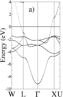
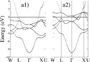
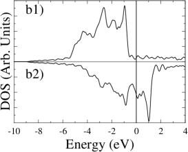
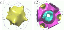
The band structure, the corresponding DOS and the Fermi surface of fcc Cu is presented in figure 2 (the Fermi surface is from reference [58]). The main feature of the dispersion of Cu is the presence of two rather different bands. The first is a high dispersion broad band with a minimum at the point eV below the Fermi level, which then re-emerges at the edge of the Brillouin zone at the and points. The second is a rather narrow eV wide band that extends through the entire Brillouin zone 1.5 eV below . By analyzing the orbital content of these two bands within a tight-binding scheme [59] one can attribute the broad band to and the narrow one to electrons. This is in agreement with the intuitive picture of the electrons much more tightly located around the atomic core and with an atomic-like configuration. Clearly there is hybridization for energies around the position of the band, which creates band distortion. However the hybridization occurs well below and therefore the Fermi surface is entirely dominated by electrons and appears rather spherical (figure 2c).
The situation is rather different in ferromagnetic metals. Since the nominal atomic configuration of the shell is , and respectively for Ni, Co and Fe the Fermi level of an hypothetical paramagnetic phase lays in a region of very high density of states. For this reason the material is Stoner unstable and develops a ferromagnetic ground state. In this case the electron energies for up and down spins are shifted with respect to each other by a constant splitting , where is approximately 1.4 eV in Fe, 1.3 eV in Co and 1.0 eV in Ni. More sophisticate DFT calculations show that the simple Stoner picture is a good approximation of the real electronic structure of Ni, Co and Fe.
The main consequence of this electronic structure on the transport properties comes from the fact that the DOS at the Fermi level, and therefore the entire Fermi surface, for the up spins (usually called the majority spin band) is rather different from that of the down spins (minority spin band). This difference is more pronounced in the case of strong ferromagnet, where only one of the two spin bands is entirely occupied. An example of this situation is fcc Co (the high temperature phase), whose electronic structure is presented in figure 3. It is important to observe that the majority spin band is dominated at the Fermi level by electrons, while the minority by electrons. With this respect the electronic structure (bands, DOS and Fermi surface) of the majority spin band looks remarkably similar to that of Cu.
Finally it is worth mentioning that there are materials that at the Fermi level present a finite DOS for one spin specie and a gap for the other. These are known as half-metals [60] and are probably among the best candidates as materials for future magneto-electronics devices.
2.2.2 Basic transport mechanism in a magnetic device
Let us consider the prototypical GMR device: the spin-valve. A spin valve is formed by two magnetic layers separated by a non-magnetic spacer. Usually the magnetic layers are metallic (typically Co, Ni, Fe or some permalloy), while the spacer can be either a metal, a semiconductors, an insulator or a nanoscale object such as a molecule or an atomic constriction. The typical operation of a spin-valve is schematically illustrated in figure 4. Usually the two magnetic layers have a rather different magnetic anisotropy with one layer being strongly pinned and the other free to rotate along an external magnetic field. In this way the magneto-transport response of the device can be directly related to the direction of the magnetization of the free layer. In our discussion we consider only the two extreme cases in which the two magnetization vectors are either parallel (P) or antiparallel (AP) to each other.

Here I will describe the current flowing perpendicular to the plane (CPP) since this is the relevant current/voltage configuration for transport through a nanoscaled spacer. However in the case of metallic spacer another possible setup is with the current flowing in the plane (CIP), as in the present generation of read/write heads used in magnetic data storage devices. As a further approximation I assume the two spin current model [39]. This is justified by the fact that a typical CPP spin-valve is usually shorter that the spin-diffusion length.
To fix the idea consider a Co/Cu/Co spin-valve, and let us follow the path of both the electron spin species across the device. The Fermi surfaces line up for both the P and AP cases are presented in figure 5.
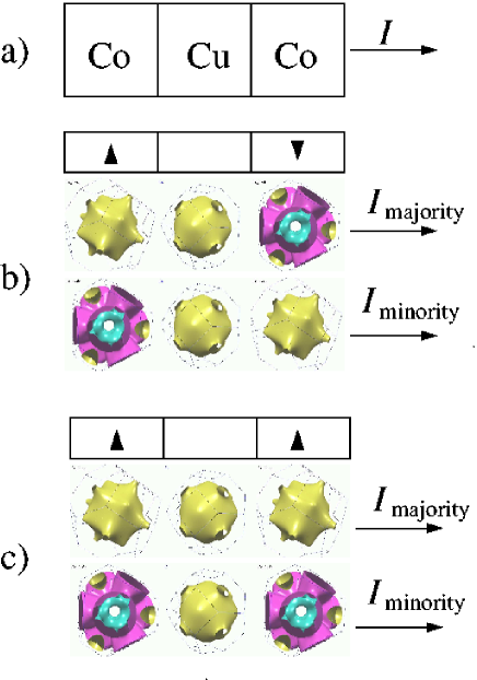
In the AP case the magnetization vector of the two magnetic layers points in opposite directions. This means that an electron belonging to the majority band in one layer, will belong to the minority in the other layer. Consequently in the AP case both the spin currents (usually called the spin channels) arise from electrons that have traveled within the Fermi surface of Cu and of both spins of Co. In contrast in the P case the two spin currents are rather different. The spin up current is made from electrons that have traveled within the Fermi surfaces of Cu and of the majority spin Co, while the down spin current from electrons that have traveled within the Fermi surfaces of Cu and of the minority spin Co.
If we naively assume that the total resistance of the device can be obtained by adding in series the resistances of the materials forming the device (resistor network model) we obtain:
| (2.4) |
| (2.5) |
where and are the resistance for the parallel and antiparallel configuration respectively, is the resistance of the Cu layer and and are the resistance of the Co layer for the majority () and the minority () spins. Usually , hence . This produces the GMR effect.
Conventionally the magnitude of the effect is given by the GMR ratio defined as:
| (2.6) |
This is usually called the “optimistic” definition (since it gives large ratios). An alternative definition is obtained by normalizing the resistance difference by either or ; in this last case is bounded between 0 and 1.
The discussion so far is based on the hypothesis of treating the spin-valve as a resistor network. This is strictly true only if , where is the typical thickness of the layers forming the spin-valve, but in general adding resistances in series may not be correct. However it is also clear that the magnitude of the magnetoresistance depends critically on the asymmetry of the two spin currents in the magnetic material, which ultimately depends on its electronic structure. It is therefore natural to introduce the concept of spin polarization of a magnetic metals as
| (2.7) |
where is the spin- contribution to the current. Clearly and are not directly observable and must be calculated or inferred from an indirect measurement. Unfortunately the way to relate the spin-current to the electronic properties of a material is not uniquely defined and depends on the particular experiment. This is why it is crucial to analyze the equation (2.7) for different situations.
2.2.3 Diffusive Transport
As brilliantly pointed out by Mazin [61], the relation between the spin-polarization of a magnetic material and its electronic structure depends critically on the transport regime that one considers. Let us start by looking at the diffusive transport. Here the phase coherence length is rather short and quantum interference is averaged out. The transport is then described by the Boltzmann’s equations, which govern the evolution of the electron momentum distribution function [62]. Within the relaxation time approximation [30], assuming that the relaxation times does not depend on the electron spin the current is simply proportional to , where and are the density of states at the Fermi level and the Fermi velocity respectively.
This leads us to the “” definition of the spin-polarization:
| (2.8) |
Values of for typical transition metals are reported in table 1 [63, 64, 65].
| (%) | (%) | (%) | |
| Fe | 20 | 30 | 60 |
| Ni | 0 | -49 | -82 |
| CrO2 | 100 | 100 | 100 |
| La0.67Ca0.33MnO3 | 92 | 76 | 36 |
| Tl2Mn2O7 | -71 | -5 | 66 |
2.2.4 Ballistic Transport
In this case is much longer than the size of the magnetic device. The energy is not dissipated as resistance in the device and the current can be calculated using the Landauer formalism [66, 67, 68]. I will talk extensively about this approach in the next sections while here I just wish to mention that in the ballistic limit the conductance, and hence the current, are simply proportional to . Moreover in the Landauer approach, as we will see, the electron velocity and the density of states exactly cancel. This means that is just an integer proportional to the number of bands crossing the Fermi level in the direction of the transport, or alternatively to the projection of the Fermi surface on the plane perpendicular to the direction of the transport (for a rigorous derivation see reference [69, 70]).
This leads to the “” definition of spin-polarization
| (2.9) |
2.2.5 Tunneling
It is generally acknowledged that in tunneling experiments the GMR ratio of the specific device is given by some density of states. This was firstly observed by Jullier almost three decades ago [71] and it is based on the fact that typical tunneling times are much faster then , with the length of the tunneling barrier. This means that the electron velocity in the metal is irrelevant in the tunneling process. Although it is now clear that the relevant density of states for magneto-tunneling processes is not necessarily that of the bulk magnetic metal, but it must take into account of the structure of the tunneling barrier and of the bonding between the barrier and the metal [72], we can still introduce the “” definition of polarization:
| (2.10) |
Clearly the three definitions may give rise to different spin-polarizations, since the relative weight of and is different. In particular favors electrons with high density, while electrons with high mobility. In magnetic transition metals, where high mobility low density electrons coexist with low mobility high density electrons, these differences can be largely amplified. In principle one can speculate around materials that are normal metals according to one definition and half-metals according to another. This is for instance the case of La0.7A0.3MnO3 with A=Ca, Sr, .. [60], in which the majority band is dominated by delocalized eg states and the minority by localized t2g electrons. Therefore La0.7A0.3MnO3 is a conventional ferromagnet according to the definitions and and it is an half-metal according to .
2.2.6 Andreev Reflection
Andreev reflection is the relevant scattering mechanism for sub-gap transport across an interface between a normal metal and a superconductor [73]. The main idea is that an electron incising the interface from the metal side, can be reflected as a hole with opposite spin leaving a net charge of inside the superconductor. In the case of normal metal the efficiency of this mechanism is solely given by the transparency of the interface. In contrast for magnetic metals, the Fermi surface of the incident electron and that of the reflected hole are different since their spins are opposite. This leads to a suppression of the Andreev reflection and therefore to a way for measuring the spin polarization of a magnetic metal.
Unfortunately also in the case of Andreev reflection it is not easy to relate the measured polarization with the electronic structures. In the case of a tunneling barrier between the magnetic metal and the superconductor, then the spin polarization is that given by and indeed the values obtained from Andreev measurements [74] agree rather well with those estimated from diffusive GMR experiments [40].
In contrast in the case of ballistic junctions the situation is more complicated. Intuitively one would guess that the degree of suppression of the Andreev reflection in a magnetic metal is proportional to the overlap between the Fermi surfaces of the two spin-species [75]. In reality the transmittivity of the interface and the nature of the bonding at the interface enters in the problem [61] and an estimate requires an accurate knowledge of the details of both the materials and the interface [76]
2.2.7 The spin-injection problem
Spin injection is one of the central concepts of spintronics in semiconductors [11]. The main idea is to produce some spin-polarization of the current flowing in a normal semiconductor by injecting it from a magnetic material. This is of course very desirable, since the spin-lifetime in semiconductors is extremely long, and coherent spin manipulation is envisioned.
From a fundamental point of view one has the problem to transfer spins across systems with very different electronic properties. In particular the huge difference in DOS at the Fermi level between an ordinary semiconductor and a magnetic transition metal, has the important consequence that the two materials show very different conductivities. This sets a fundamental limitation to spin-injection, or at least to the production of semiconductor-based GMR-like devices. In fact, if one describes the magnetic response of such devices in terms of the resistor model, it is easy to see the large spin independent resistance of the semiconductor will dominate over the small spin dependent resistances of the magnetic metals. Clearly the total resistance will be very weakly spin-dependent (for a more formal demonstration see reference [77]).
Although several schemes have been proposed to overcome this problem including spin-dependent barriers at the metal/semiconductor interface [78], and ballistic devices [79], spin-injection from magnetic metals remains to date rather elusive [80]. A significant breakthrough comes with the advent of diluted magnetic semiconductors since all semiconductor devices can be made, avoiding any resistance mismatch. Indeed spin-injection in all-semiconductor devices has been demonstrated [81, 82].
2.2.8 Crossover between different transport regimes
The classification of the different transport regimes that I have provided so far should not be taken as completely rigorous and one may imagine situations where the electrons in a device behave ballistically at low temperature and diffusively at high temperature. In this cases, unless a microscopic theory is available, it becomes rather difficult to correlate the electronic structure of the device with its transport properties. For instance consider a magnetic multilayer at a temperature such that the phase coherent length is longer than the individual layer thickness. In this case the transport will be ballistic up to and therefore it will depend on the electronic structure of as many layers as those comprised in one phase coherent length. These may include interfaces between different materials. Thus the transport will not depend on the electronic properties of the constituent materials individually, nor on the electronic structure of the whole device.
These are among the most difficult situations that a theory can address, since some hybrid methods crossing different transport regimes are needed. At present an efficient ab initio theory for spin-transport, and in general for quantum transport, capable to span across different length scales is not available.
2.3 Spin-transport at the atomic level
Most of the concepts introduced in the previous sections are usually a good starting point for describing spin-transport at the atomic scale. The main idea is now to shrink the dimensions of the device in such a way that its sensitive part will be of a size comparable with the Fermi wave-length. In this case the transport is ballistic and depends critically on the entire device. Therefore it can be hardly inferred from the properties of its components, such as the spin-polarization of the current/voltage electrodes.
Let us use again the spin-valve as a prototypical example, and consider two magnetic bulk contacts separated by an atomic scale object. This can be a point contact or for instance a molecule. There are two main differences with respect to the bulk case: 1) the Fermi surface of the spacer can be highly degenerate, in the extreme limit collapsing into a single point, 2) the coupling between the magnetic surfaces and the spacer can be strongly orbital dependent. The crucial point is that in both cases the transport characteristics will be given by local properties of the Fermi surfaces of the magnetic material, which means either from a particular region in -space, or a particular orbital manifold.
Here I will illustrate only the first concept, since I will discuss extensively the second later on. Consider figure 6 where I present an hypothetical device formed by two metallic surfaces sandwiching a spacer whose Fermi surface is a single point (the point). For the sake of simplicity I consider a model ferromagnet, namely a single orbital two-dimensional simple cubic lattice, with Fermi surfaces centered at the band center and at the band edges respectively for majority and minority spins. In this case the Fermi surface of the spacer overlaps only with the majority Fermi surface of the magnetic material. For this reason we expect zero transmission for the minority spins and for the antiparallel configuration, leading to an infinite GMR ratio. Note that this is the same result that one would expect in the case of half-metallic contacts [83], although none of the materials here is an half-metal.

2.3.1 Magnetic point contacts
Point contacts are usually obtained by gently breaking a metallic contact thus forming a tiny junction comprising only a few atoms [84]. In the extreme limit of single atom contact the junction remains metallic but its resistance is given by the electronic structure of that particular atom. A vast amount of experimental data is nowaday available for point contacts constructed from noble metals like Au (for a comprehensive review see [84]) since their large malleability and low reactivity.
Recently there was a considerable interest in magnetic point contacts, since they offer the unique chance to study spin transport at atomic scale, and they may be used to construct ultra-small and ultra-sensitive magnetic field sensors. Indeed very large GMR ratios have been measured [22, 23, 24], although there is at present a large debate on whether the effect is of mechanical or electronical origin. As a general feature transport in magnetic point contact is expected to be ballistic with both and electron contributing to the current. Moreover since the metallic nature of the contacts and the small screening length local charge neutrality is expected.
2.3.2 Molecular Spin transport
The growing interest in interfacing conventional electronic devices with organic compounds has brought to the construction of spin-valves using molecules as a spacer. These include carbon nanotubes [19, 20], elementary molecules [21, 26] and polymers [25]. Spin-transport through these objects can be highly non-conventional and vary from metallic-like, to Coulomb-blockade like, to tunneling-like. Moreover the molecule can be either chemisorbed of physisorbed depending on the molecular end groups, and the same spacer can give rise to different transport regimes.
In this case the simple requirement of local charge neutrality is not enough to describe the physics of the spacer and an accurate description of the drop of the electrostatic potential across the device is needed. Note that the transport can still be completely ballistic, in the sense that the electrons do not change their energy while crossing the spacer.
A more complicate situation arises for polymer-like spacers. In most polymers in fact the transport is not band transport but it is due to hopping and it is associated with the formation and propagation of polarons [85]. Clearly this adds additional complication to the problem since now the electronic and ionic degrees of freedom cannot be decoupled in the usual Born-Oppenheimer approximation. At present there is very little theoretical work on spin-transport in polymers.
2.3.3 Dynamical effects: Magnetization reversal and Domain Wall motion
The GMR effect demonstrates that the electrical current depends on the magnetic state of a device. Of course it is interesting to ask the opposite question: “can a spin current change the magnetic state of a junction?”. The answer is indeed positive and experimental demonstrations of current-induced magnetization switching [86] and current induced domain-wall motion [87] are now available.
The main idea, contained in the seminal works of Berger, is that a spin polarized current can exert both a force [88] and a torque [89] on the magnetization of a magnetic material. The force is produced by the momentum transfer between the conduction electrons and the local magnetic moment, and it is due to the electron reflection. This can be understood by imagining an electron at the Fermi energy completely reflected by a domain wall. In this case the electron transfers a momentum ( is the Fermi wave vector) to the domain wall, therefore producing a force. Thus the force is proportional to both the current density (number of electrons scattered) and the domain wall resistance (momentum transferred per electron). Since the domain wall resistance is usually rather small, unless the domain wall is rather sharp, this effect is not negligible only for very thin walls.
In contrast the torque is due to the spin transfer between the spin-current and the magnetization and it is proportional to , where is the local magnetic moment and is the spin-density of the current currying electrons. This effect is dominant for thick walls, where the spin of the electron follow the magnetization adiabatically.
Although several semi-phenomenological theories are available [90] an ab initio formulation of these dynamical problems has not been produced yet. A first reason for this is that do date very few algorithms for spin-transport at microscopic level have been produced; a second and perhaps the most important one is that to date there is not a clear formulation for current-induced forces, and specifically for current-induced magnetic forces. The problem of calculating the domain wall motion or the magnetization switching from a microscopic point of view is rather analogous to the problem of calculating electromigration transition rates. This is particularly demanding since it is not clear whether or not current induced forces are conservative [91].
3. Transport Theory: Linear Response
3.1 Introduction: Tight-Binding Method
In this section I will develop the formalism needed for computing spin-transport using first principles electronic structures. Throughout the derivation of the different methods I will always make the assumption that the Hamiltonian of the system can be written in a tight-binding-like form, or equivalently that the wavefunction can be expanded over a finite set of atomic orbitals. This is a rather general request that in principle does not set any limitations on the origin of such Hamiltonian nor on the level of accuracy of the calculation.
The main idea behind the tight-binding method (see for instance [31, 51, 59]) is that the wave-function of an electronic system can be written as a linear combination of localized atomic orbitals , where labels the position of the atoms and is a collective variable describing all the relevant quantum numbers (i.e. ). The specific choice of the basis set depends on the particular problem. A typical choice is to consider a linear combination of atomic orbitals (LCAO)
| (3.1) |
where is the radial component depending on the principal quantum and the angular momentum , and is a spherical harmonic describing the angular component. This latter depends also on the magnetic quantum number .
For a periodic system the wave-function is then constructed as a Bloch function from the localized basis set
| (3.2) |
where are expansion coefficients, the sum runs over all the lattice sites and , with the number of atomic sites and the number of degrees of freedom per site. If one now substitutes in the Schrödinger equation and then projects over , he will find the following matricial equation for the coefficients (secular equation)
| (3.3) |
where is the energy and the Hamiltonian. This is usually written in the compact form
| (3.4) |
where we have now introduced the Hamiltonian and overlap matrices and .
Up to this point the formalism is rather general. The specific Hamiltonian to use in the equation (3.4) depends on the problem one wishes to tackle and on the level of accuracy needed. In general there are two main strategies: 1) non-self-consistent Hamiltonian, and 2) self-consistent Hamiltonian. In the first case one assumes that the matrix elements of and can be written in terms of a small subset of parameters either to calculate or to fit from experiments [59]. In addition one usually assumes that the matrix elements of both and vanish if the atoms are not in nearest neighboring positions (nearest neighbors approximation). The Hamiltonian is then set at the beginning of the calculation and no additional iterations are needed. This approach is rather powerful for bulk systems where good parameterizations are available [92, 93], and it is computationally attractive since the size of the calculation scales linearly with the system size (sub-linearly in the case of some transport applications [55]).
In contrast in self-consistent methods the Hamiltonian has some functional dependence on the electronic structure (typically on the charge density), and needs to be calculated self-consistently. These methods are intrinsically more demanding since several iterations are needed before the energy spectrum can be calculated, although the final computational costs can vary massively depending on the specific method used [46].
Throughout this section I will consider non-self-consistent methods, while all the next sections will be devoted to the self-consistent ones. One important approximation, to the equation (3.4) is to assume that basis functions located at different sites are orthogonal. In this case and the secular equation reads
| (3.5) |
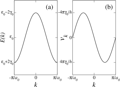
As an example consider an infinite linear chain of hydrogen atoms (see figure 7) described by a single-orbital orthogonal nearest neighbor tight binding model. In this case the basis set is simply given by the H 1 orbital where is an integer spanning the positions in chain ( with the lattice constant) and the only not vanishing matrix elements are:
| (3.6) |
which are called respectively the on-site energy and the hopping integral. Finally from the equations (3.2) and (3.5) it is easy to see that ()
| (3.7) |
and
| (3.8) |
with to be taken in the first Brillouin zone , and . A picture of the dispersion relation is presented in figure 7.

3.2 The Landauer formula
Here I will derive a general relation between the conductance of a ballistic conductor and its scattering properties. This relation is known as the Landauer formula and it is at the core of modern transport theory [66, 67].
3.2.1 Current and orbital current
Let us consider again the case of an infinite hydrogen chain discussed before and ask ourselves the question “what is the current carried by one Bloch function?”. In order to answer this question I will calculate the time evolution of the density matrix associated to a particular time-dependent quantum state . This simply reads
| (3.9) |
where on the left hand side I have used the time-dependent Schrödinger equation . Without any loss of generality one can expand the generic state over the LCAO basis
| (3.10) |
and obtain
| (3.11) |
This is the fundamental equation for the time evolution of the density matrix written in a tight-binding-like form, where are the time dependent expansion coefficients.
In order to work out the current through the H chain we need to consider the evolution of the charge density at a specific site . This is obtained by taking the expectation value of both sides of equation (3.11) over the state
| (3.12) |
Finally recalling that I am considering the first nearest neighbor orthogonal tight-binding approximation, I obtain
| (3.13) |
with
| (3.14) |
and
| (3.15) |
We can now interpret the results of equation (3.13) in the following way. The change in the charge density at the site is the result of two currents, one given by electrons moving from right to left and one given by electrons moving from left to right . The net current through the chain is then given by (note that here I am considering the current in units of the ).
Finally let us calculate the total current carried by a Bloch state. In this case it is simple to see that the expansion coefficients of the wave-function (3.10) are
| (3.16) |
and the corresponding currents
| (3.17) |
and
| (3.18) |
where is the chain length () and we have introduced the group velocity . Therefore in the case of a pure Bloch state the current is exactly zero. This is the result of an exact balance between left- and right-going currents. However it is worth noting that the individual currents and are not zero and they are indeed proportional to the group velocity associated to the Bloch state. This suggests that, although there is no net current, it may be possible to associate a conductance to this single quantum state. However the notion of conductance needs the introduction of the notion of bias voltage, or more generally of chemical potential difference. This will be introduced in the next section through the Landauer formula.
Before finishing this section I would like to make a final remark on the actual derivation of the equation for the current. Here I have projected the time evolution of the density matrix over a specific basis set, representing an atomic orbital located at an arbitrary site. In this case the choice of the basis function to project on is immaterial since we have only one degree of freedom per atom, and one atom per unit cell. In the case of more than one degree of freedom per unit cell (the cell may contain more that one atom, and each atom can be described by more than one orbital), this choice becomes more critical. In general the current calculated from the equations (3.17) and (3.18) depends on the specific orbital used in the projection, and it is usually defined as “orbital current” or “bond current” [54]. Orbital currents associated to different orbitals are usually different. This may lead to the erroneous conclusion that the current in not locally conserved. Indeed this feature originates from the incompleteness of the LCAO basis set. To overcome the problem a working definition is that of “current per cell”, where the total current is obtained by integrating all the orbital currents of those orbitals belonging to a unit cell (special care should be taken in the case of non-orthogonal tight-binding). In this way the current is conserved “locally” only over a unit cell. This basically means that the “most local” measurement of the current allowed by our basis set is that over the whole unit cell.
3.2.2 Landauer Formula
The crucial aspect of the scattering theory of electronic transport is to relate the scattering properties of a device, and therefore its electronic structure, to the current flowing through the device. This is the main result contained in the Landauer formula. Let us follow the original Landauer’s idea [66, 67]. Consider a device formed by two bulk contacts that act as current/voltage electrodes, connecting through a scattering region (see figure 8). The main assumptions behind the Landauer formula are the following: 1) the two current/voltage probes act as electron reservoirs feeding uncorrelated electrons to the central region at their own chemical potentials, 2) the difference between the chemical potential of the left and right lead is such that , 3) electrons can be fed to and absorbed from the scattering region without any scattering. Under these assumptions it is easy to calculate the current between the two leads.

Let us further assume that the scattering region, if extended to infinite, supports only one Bloch state. In this state the current is given by the product of the current associated to a single Bloch state times the number of states contained in the energy window between the two chemical potentials
| (3.19) |
where is the DOS. It is now important to note that the DOS can be easily written in terms of group velocity
| (3.20) |
and therefore the current becomes
| (3.21) |
Finally if one introduced the bias voltage through the chemical potential difference , it is possible to define the conductance for such a system
| (3.22) |
where the factor 2 takes into account the spin. is known as “quantum conductance”.
At this point I wish to make a few comments. The result just derived says that in the case of reflectionless electrodes the conductance through a scattering-free object is quantized in units of independently on the nature of the conductor itself. This result alone means that the whole definition of conductivity (and therefore resistivity) becomes meaningless and the only well define quantities are the current and the conductance. I also with to stress that this result arises from the exact cancellation between the group velocity and the DOS. This basically means that one should expect conductance quantum independently on the DOS or the band dispersion of the conducting electron. If we want to apply this concept to a ballistic contact formed from a magnetic transition metals, it is then clear that both and electrons can give the same contribution to the current, independently on their own dispersions.
Finally we assume that the central region is not completely scattering free, and we define and respectively as the total transmission and reflection probabilities across the scattering region (). Then the current will be given by and the conductance
| (3.23) |
Note that in general is energy dependent and since the condition sustaining the equation (3.23) is , then the relevant is that calculated at the Fermi level .
In the case of spin-dependent transport the total transmission probability is spin dependent and the total current must be written in term of the two individual spin-currents
| (3.24) |
where () is the transmission probability for majority (minority) spins.
3.2.3 Multichannel formalism
The formalism developed in the previous section is based on the assumption that in the scattering region there is only one Bloch state for a given energy. This is true in the case of most linear chains, but in general several Bloch states can be available at the same energy. The situation can be understood by considering a two dimensional regular square lattice of H atoms with lattice constant . Again we describe the system using the H 1 orbitals , where now and run respectively on the and direction (). In this case it is simple to see that the wave-functions are
| (3.25) |
and the band dispersion is
| (3.26) |
where and are respectively the on-site energy and the hopping integral, and and are the number of atomic sites in the and directions.
Let us now cut a slab along direction forming an infinite stripe containing sites in the cross section (see figure 9). In this case vanishing boundary conditions along the direction must be satisfied and the new wave-functions and dispersion now read
| (3.27) |
and
| (3.28) |
with
| (3.29) |
In this case the wave function is the product of a running wave along and a standing wave along and the system is usually denoted as quasi-1D. The band structure (see figure 9) is made from a set of one-dimensional bands along centered at energies . These are usually called mini-bands.

Since every mini-band corresponds to a Bloch state, therefore to a pure eigenvalue of the periodic system, it is possible to associate to each a current, exactly as we did for the true one dimensional case. The states are called channels. This leads us to the generalization of the Landauer formula due to Büttiker [68]. In this case we assume that the leads inject into each individual channel un-correlated electrons without any scattering. This means that, if there is no scattering also in the conductor, the conductance will now be
| (3.30) |
where is the number of channels at the Fermi level. Note that the conductance is simply obtained by counting the number of channels at the Fermi level, and that the contribution of each channel to the conductance is independently from the band dispersion of the specific channel. This is again the result of the cancellation between the group velocity and the density of state in the definition of the current per channel.
Finally, consider the case where some scattering is present in the conductor. In general the -channel traveling through the conductor from left to right has a probability of being transmitted through the scattering region in the -channel. Therefore the conductance associated to the -th channel will be
| (3.31) |
where the sum runs over all the final states. The total conductance of the whole system is then
| (3.32) |
where . This is the multi-channel generalization of the Landauer formula, that defines a complete mapping between transport and scattering properties of a device.
Finally if we define as the total probability for the -th channel to be reflected into the -th channel, from the particle conservation requirement we obtain the following relations
| (3.33) |
3.2.4 Finite Bias
In the previous sections I have established a relation between the zero-bias conductance and the scattering properties of an electronic system, here I will generalized the formulation to the case of finite bias. The treatment is not going to be rigorous, however it gives a very transparent picture of electron transport under bias.
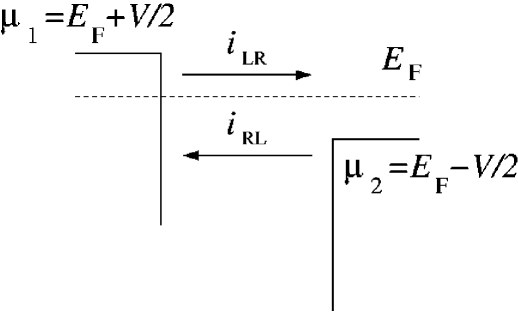
Let us consider the situation of figure 10 where two current/voltage leads are connected through a conductor. A bias voltage is applied by shifting the two chemical potentials of the leads respectively of , in such a way that . At a given energy the electron flux flowing from the left to the right of the device is simply given by the Landauer-Büttiker formula (3.32)
| (3.34) |
where is the Fermi distribution in the left-hand side lead ( is the Boltzmann constant)
| (3.35) |
The meaning of the equation (3.34) is rather transparent. It says that the flux (in units of ) from left to right is given by the total transmission probability at the energy , multiplied by the filling probability . Note that in Landauer’s spirit, when only elastic scattering is considered, backscattered electrons do not compete for final states and therefore the term needed to ensure the Pauli’s principle should not be introduced ( is the Fermi distribution of the right lead). In the same way the electron flux from right to left is
| (3.36) |
where is the total transmission probability at the energy for electrons moving from right to left. The total flux at the energy is then given by
| (3.37) |
Finally the total current is obtained by integrating over the energy. In doing so I consider the fact that when the system has time reversal symmetry (when there are no magnetic field or inelastic processes), then [94]. This leads to the expression
| (3.38) |
The equation (3.38) allows us to evaluate characteristics of ballistic devices, and it is rather useful in many situations. However it should be used with caution. First, in general the transmission coefficient is not only a function of the energy but also of the bias voltage , . This means that the scattering potential creating the quantum mechanical reflection and transmission depends on the bias applied. This dependence is weak in the case of good metals, where there is local charge neutrality, however it becomes important in non-metallic cases, like in molecules, where the electronic structure of the conductor may change substantially under bias.
The second reason is more fundamental and it has to do with the derivation of equation (3.38). In fact this has been derived assuming the Landauer formula to be valid away from and , which are the limits in which the Landauer formula is valid. Therefore the arguments sustaining equation (3.38) are compelling, but a formal derivation is still lacking [95].
3.3 Green’s Functions scattering technique
Here I will present a complete scheme to calculate ballistic transport in the linear (Landauer) limit. The technique is based on Green’s functions. These are usually preferred to the simpler wave-functions since they posses richer properties and therefore they are more versatile for transport calculations. Similar approaches based on wave-functions can be find in the literature [96].
In the linear response limit the fundamental elements of a scattering technique are the asymptotic wave-functions (“channels”) and the scattering potential. Information regarding the detailed shape of the wave-function and of the charge density inside the scattering region are not important, since the current can be determined solely from the asymptotic states. Therefore it is natural to divide the calculation into three fundamental steps: 1) the calculation of the asymptotic states, 2) the construction of an effective coupling matrix between the surfaces of the leads (the scattering potential), 3) the evaluation of the scattering probabilities and . From a numerical point of view it is also convenient to decouple the first and the second part, because the same leads can be used with different scatterers, saving considerable computation time.
3.3.1 Elementary scattering theory and matrix
The theory developed so far has been written in term of total transmission and reflection probabilities, here I will relate those to the quantum mechanical scattering amplitudes.

Consider two semi-infinite linear chains of lattice constant described by a tight-binding model with one degree of freedom per atomic site (see figure 11). The on-site energy is set to zero () and the hopping integral is (). The left-hand side chain is terminated at the atomic position and the right-hand side chain starts at the position . The chains are coupled through the hopping integral .
A general quantum state associated with such a system can be written as
| (3.39) |
with
| (3.40) |
In the equation (3.40) the normalization has been chosen in order to give unit flux (see section 3.2.1). The state is a linear combination of right- and left-moving plane waves, and a scattering state corresponds to the following particular choice of and
| (3.41) |
This means that an electron incising the scattering region placed at from the left-hand side, has a probability of being found at any positions . Similarly the probability of finding the same electron at is . and are called respectively the reflection and transmission coefficients and from particle conservation it follows the condition .
A convenient way to collect all the information regarding transmission and reflection is via the scattering matrix . In general this is defined as
| (3.42) |
where () is a vector containing the amplitudes of the quantum states approaching to (emerging from) the scattering region. Using the definition of scattering states given in equation (3.41) the matrix reads
| (3.43) |
where the quantity and are respectively the transmission and reflection coefficients for states approaching the scattering region from the right.
Clearly the expressions given above can be generalized to the case of multi-channels. A generic scattering channel can be written as a linear combination of all possible channels and the scattering amplitudes define the matrix. If , () is a real incoming (outgoing) wave-vector of energy , then an incident plane-wave in one of the leads, with longitudinal wave-vector , will scatter into outgoing plane-waves with amplitudes . If all plane-waves are normalized to unit flux, (by dividing by the square-root of their group velocities) then provided the plane-wave basis diagonalizes the current operator in the leads, the outgoing flux along channel is and will be unitary. If is real, then will be symmetric, but more generally time reversal symmetry implies . Hence, if belong to the left (right) lead, then I define reflection coefficients via (), whereas if belong to left and right leads respectively (right and left leads respectively) I define transmission coefficients ().
In this way the scattering matrix preserves the form (3.43) and and are matrices describing all possible reflection and transmission coefficients between the different channels. These are called respectively the transmission and reflection matrix. Finally the total transmission and reflection probabilities can be written as
| (3.44) |
and
| (3.45) |
3.3.2 A simple 1D example
Before going into a detailed analysis of the general scattering technique, I will present a simple example in which the main ideas are introduced. Let us consider the two semi-infinite linear chains connected through the sites and .
For an infinite chain with on-site energy and hopping integral () the retarded Green function (RGF) is simply (see for example [97])
| (3.46) |
where is the group velocity. In what follows and for the remaining of this section I will always use the adimensional -vector and I will consider only the matrix of the coefficients (the Green’s function matrix). This satisfies the Green’s equation with .
The equation (3.46) describes the RGF of an infinite system. However our main goal is to describe an electron approaching the scattering region, not one propagating through an infinite periodic chain, therefore the relevant RGF is that of a semi-infinite system. This can be computed starting from the one of the double-infinite system (equation (3.46)) by imposing the appropriate boundary conditions. Suppose the infinite system (extending from ) is terminated at the position in such a way that there is no potential for . Then the Green function with source at must vanish for (scattering channels approaching the boundaries from the left). This is achieved by adding to the expression (3.46) the following wave-function
| (3.47) |
and noting that adding a wave-function to a Green function results in a new Green function with the same causality. The final RGF for the semi-infinite system is then . Note that its value at the boundary of the scattering region is
| (3.48) |
This is usually called “surface Green’s function”. The surface Green function is independent from the position of the boundary, as expected from the translational invariance of the problem. An identical expression can be derived for the surface Green function of a semi-infinite linear chain starting at and extending to .
Going back to the initial problem, the surface Green function for two decoupled () chains facing through the sites and is an infinite matrix of the form
| (3.49) |
where () is the RGF for the left (right) semi-infinite chain. Note that has vanishing off-diagonal terms, reflecting the fact that the two chains are decoupled.
Let us now switch on the coupling between the two chains. The total Green’s function for the two chains connected through the sites and can be found by solving the Dyson’s equation
| (3.50) |
where is an infinite matrix, whose only non-zero elements are .
At this point it is important to observe that current conservation gives us the freedom to decide the “most convenient” surface to use for computing the current (in fact is is identical across any surface). Since the current across a generic surface is calculated from those matrix elements of the total Green function corresponding to the atoms facing each other through the surface, the criterion behind our choice is to select a surface for which the calculation of is easier. A particularly convenient choice is to use the surface between the atoms placed at and . In this case it is possible to show that the matrix elements , , , and can be obtained from the “reduced” Dyson’s equation (3.50) for the finite matrices and which contain only the matrix elements between the position and . In the present case these are
| (3.51) |
and
| (3.52) |
This basically establishes that the surface Green’s functions (3.51) and the coupling potential (equation (3.52)) are sufficient to compute the total Green’s function across the scattering region, and therefore the current. In this way the total Green’s function across the plane and is simply
| (3.53) |
The remaining task is to extract from the total Green function the matrix. First note that the general wave-function for an electron approaching the scattering region from the left has the form (equations (3.39) through (3.41))
| (3.54) |
where the transmission and reflection coefficients are introduced and the incoming wave-function is normalized to unit flux (see previous section). This normalization guarantees the unitarity of the matrix . Since all the information contained in are also contained in the RGF (away from the source a Green function is identical to a wave-function), the final step is to project the total Green function over the wave-function . It is possible to show (see Appendix C) that the projector that projects the retarded Green function for an infinite system over the unitary flux Bloch-function , also projects the total Green function over the (3.54). Such projector is easily calculated through the relation
| (3.55) |
and it is simply
| (3.56) |
Now I can now use to extract and . In fact by applying to and by taking the limit I obtain
| (3.57) |
from which the reflection coefficient is easily calculated
| (3.58) |
In the same way the transmission coefficient is simply
| (3.59) |
Note that the same technique can be used to calculate and for electrons incoming the scattering region from the right.
To conclude this section I want to summarize the calculation scheme presented in this example. First I calculated the Green function for an infinite system. From this I have derived the surface Green function for the corresponding semi-infinite leads by using the appropriate boundary conditions. Secondly I switched on the interaction between the leads by solving the Dyson equation with a given coupling matrix between the two lead surfaces. Finally I calculated the matrix by introducing a projector that maps the total Green function onto the total scattered wave-function.
The advantage of this technique is twofold. On the one hand the calculation of the RGF for the infinite system enables us to obtain useful information regarding the leads (density of state, conductance) and on the other hand the scattering region is treated separately and added to the leads only before evaluating the matrix. As noted above this latter aspect is particularly useful in the case in which a large number of computations of different scatterers with the same leads are needed.
3.3.3 Structure of the Green Functions
In this section I will discuss the general structure of the surface Green function for a quasi one dimensional system. I will start from a simple case, namely the two-dimensional simple-cubic lattice of H atoms discussed in section 3.2.3.
Be the direction of transport and the transverse direction comprising atomic sites. As usual is the on-site energy and the hopping integral (). By solving the Green’s equation one can find that the Green’s function for such a system is [97]
| (3.60) |
where and label respectively the and coordinates and is the longitudinal momentum. This satisfies the dispersion relation
| (3.61) |
and is the group velocity associated to the -th channel
| (3.62) |
Let us look at the structure of . The equation (3.60) can be written as
| (3.63) |
consists of the sum of all the allowed longitudinal mode (with ’s both real and imaginary) weighted by the corresponding transverse component that in this case is simply
| (3.64) |
It is then easy to identify the plane-waves with the scattering channels defined previously. Note that in the case of a one-dimensional linear chain the equation (3.63) reduces to the expression (3.46), where the .
The possible scattering channels can be then divided into four classes. The left-moving scattering channels lm (right-moving scattering channels rm) are propagating states ( is a real number) having negative (positive) group velocity. Similarly the left-decaying scattering channels ld (right-decaying scattering channels rd) are states whose wave-functions have a real exponential decay, with possessing a negative (positive) imaginary part. Note that in the case in which time-reversal symmetry is valid, the number of left- and right-moving scattering channels must be the same, as well as the number of left- and right-decaying scattering channels. Moving and decaying channels are conventionally called respectively “open” and “closed” channels. A schematic picture of all the scattering channels is given in figure 12.

Clearly there are scattering channels and the retarded Green function of equation (3.60) is obtained by summing up all open and closed channels, with their relative transverse wave-components. This structure is the starting point for our general approach.
3.3.4 General surface Green function
In this section I will present a general technique to construct the surface Green functions of an arbitrary crystalline lead. This is the first step toward a general Green’s function method for ballistic transport. An important feature of this section is that the Green function will be defined by a semi-analytic formula, which can be applied to any crystalline structure. As explained for the simple 1D case, the computation of the Green function for a semi-infinite crystalline lead starts from calculating the Green function of the associated doubly infinite system. Then the semi-infinite case is derived by applying vanishing boundary conditions at the end of the lead. To this goal, consider the doubly infinite system shown in figure 13.

Let us define as the direction of transport, and write the Hamiltonian in a block-like form along such direction. We can break down the system as a periodic sequence of “slices”, described by an intra-slice tight-binding matrix , coupled only to the nearest neighbor slices via the inter-slice tight-binding hopping matrix [98, 99]. This procedure is always possible if the lattice has some periodicity along the direction of the transport, since the interaction range of the tight-binding Hamiltonian is finite. Note that the same is true when considering non-orthogonal tight-binding models. In fact the overlap matrix has an interaction range, which is always shorter than that of the Hamiltonian matrix . This means that if is written in a block-like form, also will. In all the remaining I will consider for simplicity only orthogonal tight-binding, although the theory can be easily generalized to the non-orthogonal case. Note also that the nature of the slices does not need to be specified at this stage. They can describe a single atom in an atomic chain, an atomic plane or a more complex cell.
For such a general system, the total Hamiltonian can be written as an infinite matrix of the form
| (3.65) |
where is Hermitian and . To fix the ideas let us assume that the number of atomic orbitals describing each slice is , and therefore and are matrices. From the equation (3.4), the Schrödinger equation for this system is of the form
| (3.66) |
where is a column vector corresponding to the slice at the position with an integer and the inter-slice distance. Let the quantum numbers corresponding to the degrees of freedom within a slice be and the corresponding components of be . The Schrödinger equation may then be solved by introducing the Bloch state,
| (3.67) |
where is a normalized -component column vector and an arbitrary constant. Note that throughout this paper I will use the symbol “” to indicate the direction of the current and the symbol “” to label the transverse plane. Substituting (3.67) into the equation (3.66) gives
| (3.68) |
The task is now to compute the Green function of such a system, for all real energies, using the general Green function structure discussed in the previous section. For a given energy , the first goal is to determine all possible values (both real and complex) of the wave-vectors by solving the secular equation
| (3.69) |
In contrast to conventional band-theory, where the problem is to compute the values of for a given (real) choice of , my aim is to compute the complex roots of the polynomial (3.69) for a given (real) choice of (remember that both open and closed scattering channels enter in the definition of the Green function). Consider first the case where is not singular. Note that for real , conventional band-theory yields energy bands , , with . As a consequence, for a given choice of , to each real solution , for which the group velocity
| (3.70) |
is positive (right-moving channel), there exists a second solution for which the group velocity
| (3.71) |
is negative (left-moving channel). In the simplest case, where , one finds . Also note that to each solution the hermitian conjugate of (3.68) shows that is also a solution. Hence to each right-decaying solution possessing a positive imaginary part, there is a left-decaying solution with a negative imaginary part. For the purpose of constructing the Green function, this suggests dividing the roots of (3.68) into two sets: the first set of wave-vectors labeled () correspond to right-moving and right-decaying plane-waves and the second set labeled () correspond to left-moving and left-decaying plane-waves.
Although the solutions to (3.69) can be found using a root tracking algorithm, for numerical purposes it is more convenient to map (3.68) onto an equivalent eigenvalue problem by introducing the matrix
| (3.72) |
where is the dimensional identity matrix. The eigenvalues of are the roots , and the upper components of the eigenvectors of are the corresponding eigenvectors , . It is clear that in the case in which is singular, the matrix is not defined. However a few methods to regularize are available [100, 101] and in what follows I will assume not to be singular.
To construct the retarded Green function of the doubly infinite system, note that except at the source , is simply a wave-function and hence must have the form
| (3.73) |
where the -component vectors and are to be determined. At this point it is important to observe that the structure of the Green function of equation (3.73) is identical to the one discussed in the previous section, and that the vectors and (equivalent to the ’s of the previous section) include all the degrees of freedom of the transverse direction. Note that in representing I have chosen a slightly different notation with respect to the previous section, and I do not consider explicitly the orbital dependence on the transverse degree of freedom. It is then understood that the Green’s function between the orbital placed in the slice and the orbital placed in the slice is
| (3.74) |
Since is retarded both in and , it satisfies the Green function equation corresponding to (3.66) and is continuous at the point (see Appendix A for a detailed calculation), one obtains
| (3.75) |
The matrix is defined by
| (3.76) |
and the set of vectors () are the duals of the set (), defined by
| (3.77) |
from which follows the completeness conditions
| (3.78) |
Equation (3.75) is the RGF for a doubly infinite system. For the semi-infinite one, this must vanish at the end of the lead. In complete analogy with the one dimensional case of the previous section, consider first the left lead, which extends to and terminates at , such that the position of the first missing slice is . In order to satisfy the vanishing boundary condition at , one must subtract from the right hand side of (3.75) a wave-function of the form
| (3.79) |
where is a complex matrix, determined from the condition that the Green function vanishes at , which yields
| (3.80) |
For the purpose of computing the scattering matrix, I will require the Green function of the semi-infinite left-lead evaluated on the surface of the lead, namely at . Note that in contrast with the Green’s function of a doubly infinite lead, which depends only on the difference between and , the Green’s function of a semi-infinite lead for arbitrary is also a function of the position of the first missing slice beyond the termination point of the lead. Writing yields for this surface Green function
| (3.81) |
Similarly on the surface of the right lead, which extends to , the corresponding surface Green function is
| (3.82) |
which has been obtained by subtracting from the following wave-function
| (3.83) |
and considering ( is the position of the first slice of the right lead).
The expressions (3.81) and (3.82), when used in conjunction with (3.72) form a versatile method of determining lead Green functions, without the need to perform -space integrals or a contour integration. As a consequence of translational invariance of the doubly infinite system, the surface Green functions are independent of the position of the surface .
3.3.5 The effective Hamiltonian of the scattering region: decimation technique
I have already shown that, given the coupling matrix between the external surfaces of the leads, the Green function of the scatterer plus leads can be computed via Dyson’s equation. Generally the scattering region is not simply described by a coupling matrix between surfaces, but is a complex Hamiltonian involving all the degrees of freedom of the scatterer. Therefore it is useful to develop a method that transforms such a detailed Hamiltonian into an effective coupling matrix between the two surfaces. For structures, which possess a quasi-one dimensional geometry and a Hamiltonian which is block tri-diagonal, this can be achieved by projecting out the internal degrees of freedom of the scatterer. In the literature, depending on the context or details of implementation, this procedure is sometimes referred to as “the recursive Green function technique” or “the decimation method”, but is no more than an efficient implementation of Gaussian elimination.
Consider a scatterer composed on degrees of freedom. Then the Hamiltonian for the scatterer plus semi-infinite leads is of the form , where , are the Hamiltonians of the left and right isolated leads and a Hamiltonian describing the scattering region and any additional couplings involving surface sites of the leads induced by the presence of the scatterer. The aim of the decimation method is to successively eliminate the internal degrees of freedom of the scatterer, , to yield a effective Hamiltonian . After eliminating the degree of freedom , is reduced to a matrix with elements
| (3.84) |
Repeating this procedure times one obtains the “decimated” Hamiltonian at -th order
| (3.85) |
and after such steps, an effective Hamiltonian of the form
| (3.86) |
In this expression, () describes intra-surface couplings involving degrees of freedom belonging to the surface of the left- (right-) hand side lead and describes the effective coupling between the surfaces of the left-hand side and the right-hand side leads.
Since the effective Hamiltonian is energy dependent, this procedure is particularly useful when one wishes to compute the Green function at a given energy. It is also very efficient in the presence of short range interactions, because only matrix elements involving degrees of freedom coupled to the decimated one, are redefined. This latter aspect is very useful in the case that the scatterer has some periodicity and allows clever numerical optimizations [55].
3.3.6 The matrix and the scattering coefficients
To extract the transport coefficients from the Green function, I will use a generalization [102] of the method described in reference [103] (in particular see A.26 of [103]) to the case of non-orthogonal scattering channels. The same method has been used in the one dimensional case of section 3.3.2.
Consider first the probability current for an electron in the Bloch state (3.67)
| (3.89) |
where is the probability of finding an electron in a slice and is the corresponding group velocity. It follows that the vector
| (3.90) |
is normalized to unit flux. To compute the group velocity note that if is an eigenstate (3.65), whose projection onto slice is , then
| (3.91) | |||
| (3.92) |
where the last step follows from equation (3.68) and normalization of .
It can be shown that the states (3.90) diagonalize the current operator only if they correspond to distinct values. In the case of degenerate ’s, the current is in general non-diagonal. Nevertheless it is always possible to define a rotation in the degenerate subspace for which the current operator is diagonal and in what follows, when a degeneracy is encountered, I assume that such a rotation has been performed (see Appendix B). With this convention, the current carried by a state of the form
| (3.93) |
is simply .
It is now straightforward to generalize the analysis of [103] (end of paragraph 2.1) to the case of non-orthogonal scattering channels. Consider first a doubly infinite periodic structure, whose Green function is given by equation (3.75). For , acting on from the right with the following projector
| (3.94) |
yields the normalized plane-wave (3.90). Similarly by acting on the Green function of a semi-infinite left-lead terminating at , one obtains for , , an eigenstate of a semi-infinite lead arising from a normalized incident wave along channel . Note that the projector introduced through the (3.94) is the generalization of the one defined for the one dimensional case. In Appendix C I will formally show that the projector that projects the Green function for a double infinite system onto its corresponding wave-function, projects also the total Green function.
Thus the operator and its left-moving counterpart allow one to project-out wave-functions from the Green function of a given structure. For example, following the same procedure of the introduction, if is the retarded Green function for a scattering region sandwiched between two perfect leads whose surfaces are located at the points and , then for , the projected wave-function is of the form
| (3.95) |
where , are reflection and transmission coefficients associated with an incoming state from the left. In particular for , , one obtains
| (3.96) |
and hence
| (3.97) |
where I used the definition of the dual vector given in equation (3.77). With the same method one evaluates all the other elements of the matrix
| (3.98) |
| (3.99) |
| (3.100) |
Since the right-hand sides of (3.97-3.100) involve only the surface Green function of equation (3.87) the transport coefficients are determined. Moreover, since the above analysis is valid for any choice of the Hamiltonians and , this approach is completely general.
3.4 Alternative approach to linear response transport
In this section I will review several alternative approaches to linear response transport. They are all based on the Landauer formula, and the main differences concern the method for calculating the surface Green’s functions, and for extracting the transport coefficients. Since the field is rather vast, here I will review only those methods that have been largely used for spin-transport calculations.
3.4.1 Sharvin Conductance
A simple way to calculate the linear conductance of a nanoscaled system with a cross section smaller than and larger than the Fermi wave-length, is the calculation of the Sharvin conductance [69, 70]. The main idea is that of assuming the conductor to be scattering free and evaluating the conductance by counting the number of open channels at the Fermi level, for a system of finite cross section. These are proportional to the area of the cross section and the projections of the Fermi surface for different bands onto the plane normal to the transport direction . In this way the conductance for spin- electrons can be written as
| (3.101) |
where are the energy bands. The formula above has been derived from both the Boltzmann equation [104] and the Landauer formalism [105].
The method is clearly rather crude, since the scattering problem is not solved. However, when combined with accurate band structure calculations, it may provide useful preliminary insights. In addition it is worth pointing out that the expression (3.101) does not need a tight-binding-like Hamiltonian and it can be combined with any band structure method, such as plain-wave based DFT.
3.4.2 Recursive methods
The main idea behind recursive methods is to calculate either the wave- function or the Green’s functions of an infinite system, by “propagating” the asymptotic solution (channel) across the scattering region. Here I will explain the basic concept by using wave-functions and a simple one dimensional hydrogen chain, and I will refer to the literature for more details.
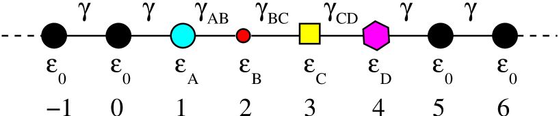
Consider two semi-infinite linear chains described by a nearest neighbors single-orbital tight-binding model with on-site energy and hopping integral (). The two chains are terminated respectively at the sites and , and are connected through four atoms with on-site energies () and hopping integrals (see figure 14). As usual the general wave function can be written as
| (3.102) |
where is the atomic orbital corresponding to the site . In complete analogy to what developed in the previous sections, it is clear that the knowledge of the coefficients over the scattering region is not necessary in order to extract the transport coefficients. The main idea is then to write the coefficients for in terms of those for . This can be achieved by “propagating” the wave function is real-space over the scattering region.
Consider the Schrödinger for the coefficient at site equation associated with the linear chain under consideration
| (3.103) |
This can be re-written as
| (3.104) |
or in the convenient matrix form
| (3.105) |
The matrix connects the coefficients of the wave function at the sites and to those at and . This is called transfer matrix and allow us to express the coefficients of a wave-function at a certain position in terms of those at another position. Thus the coefficient at and are connected to those at and by
| (3.106) |
Note that in the case of a infinite periodic system ( and ) the coefficients of the wave function are simple plane waves and the equation (3.105) simply reduces to
| (3.107) |
This is entirely equivalent to the equation (3.72) for a generic quasi-one dimensional system, once we have replaced with and with (note that in this case and therfore ). Indeed the equation (3.72) can be derived from the generalization of the transfer matrix method to multi-orbital tight-binding Hamiltonian. Hence the inverse band structure problem is entirely equivalent to finding a diagonal form for the transfer matrix .
Going back to our original problem let us suppose to have calculated the transfer matrices connecting the sites to the sites
| (3.108) |
The crucial point is that for and the coefficients of the wave function are just plane waves (channels)
| (3.109) |
This allows us to write a matrix equation for the amplitudes and
| (3.110) |
with
| (3.111) |
Finally, recalling the definition of matrix
| (3.112) |
one finds
| (3.113) |
It is then demonstrated that the transfer matrix method can fully describe a quantum mechanical scattering problem. Moreover it can be generalized to both multi-orbitals tight-binding model, in the spirit of the quasi-one dimensional systems described in section 3.3.4, and to the calculation of the surface Green’s functions (instead of the wave-functions). In particular the use of the transfer matrix method to calculate the RGF for scattering problem was introduced two decades ago by Lopez-Sancho et al. [110, 111] and then used in a large range of scattering problems [112].
An interesting use of the transfer matrix method combined with Green’s functions, is the “adlayer” method proposed by Mathon [113, 114]. Here the idea is to construct the RGF across the scattering region by propagating the surface Green function for one of the leads. In this way the scatter is add layer by layer to the lead by solving recursively the Dyson’s equation.
3.4.3 Layer KKR Methods
The Korringa, Kohn and Rostoker (KKR) method is an electronic structures method originally designed for calculating band structures of solids [115, 116] and then optimized to problems of defects and interfaces. The essential idea is to perform a muffin-tip approximation of the real ionic potential [30] and to expand the wave-function over a set of spherical harmonics. The KKR approximation consists in truncating this expansion.
Recently the method has been combined with DFT and quantum transport with good results in describing ballistic transport and tunneling. In particular large emphasis has been given to the so called layer KKR method (LKKR) [117]. Here the idea is to divide the system into layers and to “propagate” the wave-function from layer to layer with a recursive method resembling the transfer matrix technique. The final output is the electronic structure of a solid. The crucial point is that, since the algorithm is essentially recursive, there is no need of periodicity in three dimensions. This is why LKKR is suitable for transport problems. In this case one starts from a layer deep the two leads and propagates the wave function across the scattering region. Once the electronic structure is calculated, the ballistic (linear response) conductance can be extracted. Several implementations have been proposed within this scheme. These include a wave-function approach with Landauer conductance [118] and a Green’s function scheme [119, 120] with current extracted from the Kubo formula [121].
3.4.4 Wannier Functions
A Wannier function , labeled by the Bravais lattice vector , is obtained as a unitary transformation of a Bloch function of the -th band
| (3.114) |
with the volume of the unit cell and the integration extending over the entire Brillouin zone. The resulting function is an atomic orbital like function and it can be used to construct a tight-binding like Hamiltonian.
Recently a novel scheme for calculating ballistic transport using Wannier functions have been proposed [122]. The method consists first in performing a DFT calculation and then to transform the Kohn-Sham eigenvectors into a Wannier function basis set. Particular care is taken to construct rather localized Wannier functions, and the maximally localized scheme is used [123] . In this way the self-consistent Hamiltonian can be written in a tight-binding form and the ballistic transport calculated using standard Green’s function techniques. Although to my knowledge the method has never been used for spin-transport it appears as rather versatile post-processing step in standard electronic structure calculations, and it may become popular in the future.
3.4.5 Ring Geometries
One of the fundamental problems of the Landauer theory of transport is that although it is based on the scattering states and therefore on a purely quantum mechanical system, it needs the definition of two distinct chemical potentials in order to derive a relation between current and voltage. Of course the two pictures reconciliate in the zero bias limit, but a conceptual problem remains in the case of finite bias.
In recent years there have been several attempts to recast the Landauer theory in a completely Hamiltonian form. The basic idea is to map the problem of two electronic current/voltage probes coupled through a scattering region (as in the case of a two terminal transport measurement), on a macroscopically large ring with bias applied as a time-dependent vector potential (see figure 15). In this case the problem becomes completely Hamiltonian and it can be in principle solved exactly, even in the presence of strongly interacting systems [95]. Although it is not clear whether the method will be ever extended to realistic materials, several fundamental results have been obtained.
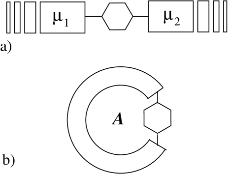
In particular Ramšak and Rejec demonstrated that for non-interacting leads connected to an interacting Fermi liquid region the zero-temperature conductance can be calculated from the variation of the ground state energy with respect to the magnetic flux [124, 125, 126]. Moreover Burke et al. in the DFT framework showed that the Landauer formula at zero bias can be recovered if the exchange correlation potential is local or semi-local [127]. Finally Gebauer and Car proposed a method in which the the density matrix of a many-electron system is propagated in time under the action of an external electric field [50, 128]. The method uses TDDFT in the master equation formulation.
3.4.6 Superconductivity
One interesting application of the linear response transport theory is in the study of sub-gap transport across superconductor interfaces. This is particularly relevant for spin-transport since it was proposed as a method for measuring the spin-polarization of magnetic metals [129, 130, 131]. As explained in the previous section the relevant scattering mechanism for sub-gap conductance across a superconductor interface is the Andreev reflection [73], where an electron is back-scattered from a superconducting interface into a normal metal leaving two electronic charges in the superconductor. This mechanism competes with normal reflection and the conductance must be calculated by taking into account the two possible scattering events.
The basis for computing the scattering coefficients is formed by the Bogoliubov de Gennes equation [132], which are obtained by diagonalizing the mean-field BCS Hamiltonian. For a non-magnetic, spin-singlet superconductor within a one dimensional single orbital tight-binding model they read
| (3.115) |
where () are the amplitudes of the electron (hole) wave function, is the superconducting gap and the sums run over nearest neighbors. The model is formally identical to two one-dimensional chains with on-site energies and hopping integrals respectively , and , , and coupled through the superconducting gap energy . Clearly in the normal (non-superconducting) region electrons and holes are not coupled and . Since the formal analogy with a normal problem, all the scattering techniques developed in the previous sections can be used also for the superconducting problem. For an extensive review I refer the reader to more specialized literature [133].
Finally the same formalism can be applied to the case of ferromagnetic materials in contact to superconductors. In this case the explicit spin-dependence of the single-particle Hamiltonian (in the Bogoliubov de Gennes spirit) must be introduced giving
| (3.116) |
where is the spin-dependent Hamiltonian describing the normal state and with the unit matrix. Note that I have now generalized the formalism to arbitrary dimensions and multiple orbitals tight-binding model, being a general matrix. In the case of a ferromagnet we have , while for a superconductor . Again all the scattering techniques developed so far can be used for calculating the linear response conductance. Finally it is important to note that the exchange coupling in magnetic transition metals is typically three order of magnitudes larger than the superconducting gap in ordinary superconductors. For this reason one does not expect the spin-polarization of the magnetic metal to change with the onset of the superconductivity, and therefore the same tight-binding parameters can be used in the normal and superconducting case. Usually one considers abrupt interfaces and both the magnetization and the superconducting parameter are taken as step functions across the interface.
4. Transport Theory: Non-equilibrium Transport
4.1 Introduction
The scattering theory outlined in the previous section is based on the simple idea of measuring the probability of an electron leaving one current/voltage probe to be absorbed by another probe. In all the discussion the details of the electronic structure of the scattering region was secondary and we were only interested in the resulting scattering potential. In actual fact I have deliberately eliminated all the information about the scattering region with the decimation scheme. Clearly this procedure compromises our knowledge of how the charge density distributes in the scattering region, and of the detailed shape of the scattering potential. At zero bias, in the limit where the Landauer approach is strictly applicable, this information is somehow immaterial, but it becomes crucial at finite bias.
In this section I will develop an alternative method to evaluate the current between two probes, which fully preserves the knowledge of the electronic charge density and potential. This method is way less intuitive and transparent than the previous one, but it has the advantage of allowing a self-consistent evaluation of the potential, and in principle to include inelastic scattering. The development will not be formal and aims to give a consistent intuitive picture of the method. More formal derivations can be find a in rather vast literature [134, 135, 136, 137, 138].
4.1.1 A simple model
Let me start with a simple example designed by Datta [139]. Consider two current/voltage probes having two different chemical potentials and and connected through an atom described by a single energy level (see Figure 16). If the energy level is in equilibrium with the first contact its occupation will be given by
| (4.1) |
In the same way the condition of equilibrium with the second contact gives an occupation . However if equilibrium cannot be established with either the first and the second probe and the average number of electrons occupying the state will be a value intermediate between and . This imbalance between the equilibrium occupation and the real occupation produces the current to flow. In fact the net flux across the left contact is proportional to :
| (4.2) |
while the flux across the right contact is
| (4.3) |
where are the transmission rate between the contact and the single energy level .

At steady state there is no net flux into or out of the energy level, thus , and one can simply derive an equation for
| (4.4) |
This allow us to finally obtain the current, by substituting equation (4.4) into one of the equations for the flux
| (4.5) |
Unless one considers very high temperatures the current will flow only if the energy level is located between the two chemical potentials. In fact if is below both and then, , while if it is above .
Note that the model developed so far provides information on both the occupation of the energy level (equation (4.4)) and the steady state current (equation (4.5)). This is a major advantage with respect to the methodology developed in the previous section, since it naturally allow us to introduce self-consistent procedures. For instance if one assumes that the position of the energy level is a function of its occupation , then one can calculate self-consistently both N and by looping over the equation (4.4), as suggested in figure 17.

4.1.2 Broadening and Green’s function
Our simple model contains already most of the aspects of a more general theory based on the non-equilibrium Green’s function method. To complete the analogy I will introduce an additional element in the description, this is the broadening of the energy level. In fact, since the energy level is coupled to the leads by the transmission rates and , its lifetime is finite and given by (). The uncertainty principle then requires the state to have an energy spread of . This is introduced by describing the DOS of the energy level as a Lorentzian function centered around
| (4.6) |
Clearly should have the property to hold only one electron, hence its energy integral is equal to one. It is then quite intuitive to re-define the expressions for the occupation and the current across the two terminals in terms of the DOS associated to as follows
| (4.7) |
| (4.8) |
where I have deliberately left the ’s inside the integral since in general the broadening can be a function of the energy . Note that the argument of the integral in equation (4.7) is nothing but the electron charge density at the steady state , and that the expression for the two terminals current can be written as
| (4.9) |
with
| (4.10) |
is simply the total transmission probability and the equation (4.9) reproduces the result obtained when starting from the two terminal Landauer theory of equation (3.38). It is also useful to rewrite the two terminal currents (4.2) and (4.3) in terms of and , since this gives us a powerful tool to generalized our formalism to multi-terminal devices. For a generic lead this can be written in a compact form as
| (4.11) |
where we have introduced the in-scattering function .
In the expression developed so far I have written both the current and the occupation of the energy level only in terms of the DOS, the electron charge density and transmission probabilities. Furthermore it is important to note that I did not introduce any notion of quantum mechanics, except for the uncertainty principle, and that all my arguments are essentially based on a system of rate equations. It is now useful to recast the previous equations in terms of a more powerful analytical tool, the single particle Green’s function
| (4.12) |
This will offer us the opportunity to generalized the simple concepts introduced so far to more complicated electronic structure and self-consistent methods. Both the DOS and the charge density can be written as a function of
| (4.13) |
| (4.14) |
where . Similarly the two terminal current is
| (4.15) |
The non-equilibrium Green’s functions (NEGF) method consists in generalizing the equation written above to more complicated electronic structures.
Before leaving this section let me summarize the philosophy adopted throughout this derivation. The main difference from scattering theory is that now I focus my attention on the energy level (the actual conductor), instead then on the leads. Hence I define the conditions for the steady state, where the current is obtained as a balance of the currents entering and leaving the conductor. Finally I recast all the formalism in terms of single particle Green’s function, which is the proper theoretical tool for bridging this simple model with the more powerful NEGF theory.
4.1.3 NEGF Method
The simple model introduced in the previous section does not describe two important aspects of a real device: the electronic structure of the contacts and the details of the scattering region Hamiltonian. These are replaced respectively by the Fermi distribution functions and by a single energy level. It is the goal of this section to bring these details back in our formalism.
Let us assume again that we can express the Hamiltonian in an orthogonal tight-binding form. In the last part of the previous section I have re-written all the fundamental quantities (energy level occupation and current) in terms of the energy level Green’s function (see equation (4.12)), and the coupling with the leads (’s). It is therefore natural to generalize to a more detailed Hamiltonian , describing all the degrees of freedom of the scattering region
| (4.16) |
where has been introduced to respect causality. In this general form the coupling of the scattering region with the left and right lead is described respectively by the left and right self-energy and . These are energy dependent matrices containing all the details of the electronic structures of the leads and their coupling with the scattering region. Therefore is formally the Green’s function associated to an effective Hamiltonian , with the self-energies taking the rôle of external potentials. It is also important to note that the self-energy matrices are in general complex quantities, with the expected result that the total number of electrons in the scattering region is not a conserved quantity. The self-energies naturally extend the idea of transmission rates introduced in the previous section and their pure complex part (1, 2) is usually called the broadening matrix
| (4.17) |
In addition the ’s possess a non-vanishing real part. These shift the energy levels of the scattering region, an effect that was neglected in the simple model.
We can then define the two terminal current as
| (4.18) |
This is similar to that of equation (4.15), where now the total transmission coefficient is obtained as the trace of . The derivation of equation (4.18) follows the same arguments of in going and out-going currents used for the derivation of its single energy counterpart (4.15), and quantities such as the in scattering matrix can be defined.
The equations (4.16) and (4.18) allow us to calculate the current once the Hamiltonian for the scattering region and the self-energies are known. While I will give an expression for the self-energies in the next section, here I would like to point out that the Hamiltonian is not always known exactly. In general its functional dependence on the electronic structure is known but its exact value needs to be calculated self-consistently. In general I will assume that depends on the single particle density matrix associated to the scattering region . This is a rather general assumption underpinning the fact that can be constructed with a single particle electronic structure method (DFT, Hartree Fock etc.). It can be viewed as a natural generalization of the dependence of the energy level on its occupation discussed in the previous section.
It is therefore important to evaluate the density matrix from the Green’s function of the scattering region. Following the analogy with our simple model the energy dependent density matrix can be written as (see equation (4.14))
| (4.19) |
while the density matrix is obtained by integrating
| (4.20) |
As in the case of the simple model we have now a clear prescription on how to construct a self-consistent calculation. Let us suppose to have calculated the self-energies and that these do not change during our self-consistent procedure (see section 4.1.4). We first compute the scattering region Green’s function (equation (4.16)) for , where the Hamiltonian is evaluated at a given initial charge density . Then from the Green’s function we calculate the new charge density (equation (4.20)), which is then used to construct the new Hamiltonian . This procedure is iterated until reaching self-consistency, that is when . At this point the scattering region Hamiltonian is known exactly and finally the current can be extracted by using the expression (4.18).
4.1.4 How to calculate the Self-energies
In this section I will present a simple argument which will enable us to evaluate the leads self-energies. Let us consider a scattering region attached to only one lead as shown in figure 18. In this case the Hamiltonian for the whole system (scattering region plus lead) is a semi-infinite matrix of the form
| (4.21) |
The corresponding RGF can be partitioned in a block structure and obtained by formal inversion of the Hamiltonian
| (4.22) |
Our task is to extract an expression for the portion , which represents the Green’s function for the scattering region attached to the lead 1. From the equation (4.22) one can write
| (4.23) |
and
| (4.24) |
From the first equation we can extract
| (4.25) |
with
| (4.26) |
Note that is the retarded Green’s function for the semi-infinite lead 1, a quantity that we have already calculated in section 3.3.4. Finally substituting Eq.(4.25) into Eq.(4.24) we derive the expression for the Green’s function of the scattering region
| (4.27) |
The expression (4.27) is identical to that of equations (4.16), which allows us to identify as the self-energy of lead 1.

Although is in principle a matrix with the number of degrees of freedom in the scattering region, in practice it will couple only a limited number of atoms (that we generally called surface atoms). This means that only surface atoms on the leads are relevant for the product , allowing us to identify with the surface Green’s function.
It is important to point out that a similar result could have been obtained by decimating layer by layer all the degrees of freedom of the lead (see for example [112]). This procedure, introduced for the first time by Lopez-Sancho et al. [110, 111] does not require the decimation of the whole semi-infinite lead and a few iterations of a recursive set of equations are sufficient. However, the recursive method nicely highlights the differences between the NEGF method and the scattering theory. With the first method one decimates the leads in order to extract the self-energies (effects of the leads on the scattering region). In the second, one decimates the scattering region in order to evaluate an effective scattering potential between the leads. Clearly the two methods are equivalent and one has to decide which is the best method for the specific problem.
4.1.5 Introducing the bias
The expression for the current given by the equation (4.18) is very similar to its Landauer-Büttiker counterpart (3.38) and essentially it involves the integration of the transmission coefficient over the bias window. However in the present case the availability of information about the charge density in the scattering region (and thus about the Hamiltonian), gives us the chance to introduce a self-consistent evaluation of the potential drop, and therefore to replace with in the expression for the current.
There are several ways of introducing finite bias in the self-consistent calculation and the details usually depend on the particular numerical implementation chosen. Here I will only provide a few general concepts.
The “effective” scattering region
The key consideration in setting up a self-consistent calculation is to observe that the potential drop will only affect a small portion of the entire device (defined as leads plus scattering region). In general the leads are metallic and one expects the electrical potential to relax rapidly to its bulk value when moving away from the surface. This is simply due to the strong electron screening properties of ordinary metals. For this reason one usually performs a self-consistent calculation of the potential drop by defining an “effective” scattering region comprising the scatterer and a few layers of the leads. The number of layers introduced in this new scattering region should be large enough to reproduce the bulk potential at the edges.
Displacing the potential in the leads
The effect of applying a finite bias over the leads is that of shifting their relative chemical potentials. This, in addition to the necessary condition of local charge neutrality, results in a relative displacement of the whole band structure of the leads. In practice one displaces the bottom of the left-hand side lead by and that of the right-hand side lead by (and the opposite for reverse bias), with the bias applied. In a tight-binding language this means shifting rigidly the Hamiltonian (=1, 2) of the leads
| (4.28) |
and in terms of self-energies it translates into the following expression
| (4.29) |
Trial potential drop and self-consistent procedure
In principle the rigid shift of the leads potential and the appropriate choice of the effective scattering region should be enough to determine the potential drop. In fact the first sets the boundary conditions and the second ensures that those boundary conditions can be met by an appropriate electrostatic calculation. At this point one needs an efficient way to solve the Poisson equation for the effective scattering region under the given boundary conditions. A conventional way is to add a linear potential drop to the Hamiltonian describing the scattering region
| (4.30) |
and then to iterate the self-consistent procedure described in section 4.1.3 once the shifted self-energies of equation (4.29) are used.
4.2 DFT method
Density functional theory (DFT) is nowadays the most popular electronic structure method among several communities. It is based on the famous Hohenberg-Kohn theorem stating that the ground state energy of a system of interacting particles is a unique functional of the single particle charge density [44]. The prescription for calculating both the charge density and the total energy is that to map the exact functional problem onto a fictitious single-particle Hamiltonian problem, known as the Kohn-Sham Hamiltonian [45]. This comprises a kinetic part, a part describing the interaction between electrons and nuclei, a classical electrostatic part and the exchange and correlation potential. This latter in principle includes all the many body effects, although its actual form in unknown.
DFT for magnetic materials
Density functional calculations for magnetic materials became widespread in the late 1970s, with a number of studies of third and fourth row transition metals [140, 141, 142]. These studies established that the local density approximation gives results that are in reasonable agreement with experiments for quantities such as cohesive energy, bulk modulus and magnetic moments, provided that spin polarization is included explicitly, by extending the LDA to the local spin density approximation (LSDA) [143]. They also noted, however, that the calculated properties are very sensitive to details of the structure and magnetic ordering, which can lead to discrepancies between the LSDA results and experiment. The most notorious of these is the well known prediction of the incorrect ground state of iron (face centered cubic and antiferromagnetic, rather than the correct body centered cubic and ferromagnetic) by the LSDA.
A number of technical developments have facilitated the study of magnetic materials, perhaps the most important being the introduction of the fixed spin moment (FSM) method [144, 145]. In the FSM method the ground state of a constrained system with a fixed magnetic moment is calculated. Not only this does speed convergence, but the total energy surface in magnetic moment/volume space can be determined, giving additional information particularly about metastable magnetic phases. Also, the implementation of Gaussian smearing [146] and related schemes have helped to speed convergence of calculations for magnetic metals with partially filled bands and complex Fermi surfaces, in which it is difficult to carry out integrals over the occupied part of the Brillouin Zone.
In parallel with these technical developments, extensions and improvements to the LSDA have also been explored. The usual generalized gradient approximation (GGA) [147] that gives improved results for non-magnetic systems do not tend to give systematic improvement for magnetic materials, although the GGA does at least predict the correct ground state for iron. For more information about these approximations see reference [148] and references therein. Finally it is worth mentioning that methods such as the LDA+U [149, 150], and self-interaction-correction [151] are specifically tailored to treat strongly correlated systems, and therefore are more appropriate for magnetic systems with narrow or bands.
DFT for transport
The use of DFT in quantum transport algorithms has certainly a recent history. Most of the early activity has been focused on using DFT for extracting parameters for simpler models (tight-binding) and in conjunction with Landauer theory. Only in the last five years the connection between DFT and self-consistent finite-bias transport has become strong. The general idea is to use DFT as a single-particle theory. In this way the Kohn-Sham eigenstates are interpreted as single particle excitations and non-equilibrium transport methods can be applied. This is clearly not completely satisfactory, since formally the Kohn-Sham eigenstates do not represent an effective single particle theory, but only the eigenstates of the fictitious Kohn-Sham Hamiltonian. Nevertheless they often reproduce rather well the single particle excitations and one expects that in the same limit also the transport will be well described. The discussion on this and related issues is at present very active.
To date there are a few codes available for performing DFT-transport. Most of them are based on the NEGF method and they essentially differ for the numerical implementations considered. To our knowledge there is only one fully self-consistent DFT code, which can deal with spin-polarized systems. This is Smeagol, a code developed by the present author and collaborators and entirely designed for magnetic materials. In what follows I will provide a short description of Smeagol and the other DFT codes available, and finally of a few non-DFT based transport code.
4.2.1 Smeagol
Smeagol (Spin and Molecular Electronics on Atomically Generated Orbital Landscape) [100, 101] is a fully spin-polarized code, which combines the NEGF method with the DFT code SIESTA [57]. SIESTA is a numerical implementation of DFT constructed on a non-orthogonal localized atomic orbital basis set [152]. This, in conjunction with the use of efficient scalar relativistic Troullier-Martins pseudopotentials [153] with non linear core corrections [154], makes SIESTA particularly suitable for handling systems with a rather large number of degrees of freedom. It is therefore ideal for typical magneto-transport problems.
Since the final product of SIESTA is a tight-binding like Hamiltonian, SIESTA can be easily interfaced to the NEGF method discussed previously. This is implemented into Smeagol. To my knowledge Smeagol is the only fully spin-polarized code available at present. This goes beyond the use spin polarized exchange correlation potentials, including the non-collinear spin option, since magnetic materials carry additional difficulties with respect to non-magnetic systems. In fact the localized electrons co-exist in the valence with the extended electrons making the Hamiltonian matrix rather sparse. In this situation conventional recursive methods have problems to converge the surface Green’s functions of the leads, which are essential to construct the self-energies. In Smeagol surface Green’s functions are calculated using the semi-analytical expression [102] discussed in section 3.3.4, after having regularized .
Finally it is worth mentioning the way in which Smeagol calculates the potential drop. This is obtained by solving the Poisson equation for the scattering region. However, instead of using a real-space method (perhaps more desirable) Smeagol does that in -space, making use of the fast Fourier transform algorithm. For this purpose a supercell containing the scattering region is constructed and a saw-like external potential is superimposed at any iteration.
4.2.2 Other DFT codes
Several DFT-based non-equilibrium transport codes are available, although at present none of them has the ability to deal with spin-polarized systems. In what follows we list a few of them with a short description of their main technical details.
The McDCal Program
McDCal is a package created in Guo’s group at the McGill University [155]. It combines NEGF method with a numerical implementation of DFT based on pseudopotentials and the Fireball linear combination of atomic orbitals basis set [156]. The self-energies of the leads are calculated by using a technique very similar to that of section 3.3.4, while the electrostatic problem is addressed by solving the Poisson equation for the Hartree potential using a real-space multigrid approach [157]. McDCal has been very successful in describing transport through molecular objects [158, 159] and metallic nanowires [160].
TranSIESTA
TranSIESTA [161] is a combination of NEGF with the DFT code SIESTA [57]. In many respects TranSIESTA is similar to both Smeagol and McDCal. The electrostatic potential is calculated by solving the Poisson equation in -space superimposing to the Hartree potential a linear potential ramp, while the surface Green’s functions are calculated by direct integration. Although it does not have spin-polarized functionalities, TranSIESTA allows the calculation of current-induced forces [162] and therefore the study the mechanical stability of current-carrying nanodevices.
GECM transport
Recently the NEGF method has been implemented in conjunction with the quantum chemistry package Gaussian98 [163] to give the Gaussian embedded-cluster scheme (GECM) for quantum transport [164, 165]. One of the main difference of this methods with other existing algorithms is the use of tight-binding Bethe lattice [166] when constructing the self-energies. The self-energy of a Bethe lattice is essentially analytical and somehow it averages out effects like disorder of thermal smearing. For this reason usually both the transmission coefficients and the - characteristics are rather smooth.
Lippmann-Schwinger method
One of the early approach to DFT-based transport consists in the solution of the Lippmann-Schwinger equation involving the Green’s function for a biased metallic junction [167]. The method is implemented in a plane-wave DFT framework and also in this case there is a self-consistent procedure for evaluating the potential drop. The method has been extensively used for calculating fundamental transport properties of elementary molecules [168].
Nanohub
One of the world-leading group in theory of quantum transport is the Purdue University group. Over the last few years they have developed a series of packages for calculating realistic - characteristics at different level of complexity, including DFT methods [138]. Part of this work can be found at the web-site www.nanohub.org.
4.3 Transport using non DFT electronic structure methods
In addition to DFT-based methods recently a few novel computational tools have been produced. The purposes of these tools are various, from introducing strong correlation effects in the calculation, to lightweight semi-empirical algorithms capable to handle a large number of degrees of freedom. A quick summary of these codes is reported here.
4.3.1 Semi-empirical TB
Semi-empirical tight-binding methods are half-way between fully self-consistent localized basis DFT algorithms and non self-consistent Hamiltonians. The main idea is to expand the Kohn-Sham Hamiltonian written on a localized atomic orbital basis set about a reference charge density [52, 169]. Thus one obtains a second order expansion in a tight-binding like form. This depends on a series of parameters that can be either calculated directly or fitted from LDA calculations. In addition, usually the on-site Coulomb potential is replaced by Hubbard terms, in order to correct the LDA inability to evaluate correctly the on-site Coulomb energy. Since the Hamiltonian is written in a tight-binding like form this method can be readily implemented in a NEGF scheme for transport. A code developed by the group of Di Carlo is currently free available (http://icode.eln.uniroma2.it) [170].
4.3.2 Configuration Interaction method
In an attempt to go beyond DFT in describing the electronic transport a novel method based on the configuration interaction scheme has been recently proposed [42]. Here the many-body wave-function is expanded as spin-dependent Slater determinants and the scattering boundary conditions are obtained in terms of Wigner function. From the results available to date it is clear that many-body effects may be relevant for transport through small molecules, although it is not obvious whether the method (quite computational intensive) may be upscaled to more complicated systems.
4.3.3 TDDFT method
Despite the success of DFT-based quantum transport codes, several important questions at the foundation of the method still remain. In particular the use of the Landauer formalism out of equilibrium and the interpretation of the Kohn-Sham eigenstates as single particle states, are somehow not completely under control. Recently a new DFT theorem encompassing transport at finite bias has been proved [50, 128]. This is based on the reformulation of TDDFT including dissipation to phonons using an associated Kohn-Sham master equation. The method is a radical departure from conventional DFT-based methods for quantum transport. However at present it is difficult to forecast how easily efficient numerical implementations handling a large number of degrees of freedom may be constructed.
5. Results
In this section I will review the main successes of ab initio transport theory in describing magnetic devices. I will start with the more conventional GMR effect in magnetic multilayers, which is at the basis of the “spintronics era”, and its tunneling counterpart, the tunneling magnetoresistance (TMR). Devices based on these two effects are already in production (GMR-based read heads for magnetic data storage) or are at a prototype level (TMR-based Magnetic Random Access Memories: MRAM). Then I will discuss atomic scaled magnetic junctions, made either from metals such as magnetic point contacts or from organic molecules. These will probably drive the next revolution in the field and appear very attractive to theory since their reduced dimensions offer the unique possibility to compare directly predictions with experiments. Finally I will briefly discuss a very recent development, the magnetic proximity effect. This is the induction of a net magnetization in a non-magnetic material when brought into contact with a magnetic one.
5.1 GMR
As already mentioned the giant magnetoresistance (GMR) effect is the drastic change in resistance of a magnetic multilayer when a magnetic field is applied. This is related to the change of the mutual orientation of the magnetic moments of the magnetic layers.
In metallic systems adjacent magnetic layers are magnetically coupled to each other, through the non-magnetic ones. The sign of this exchange coupling, discovered by Stuart Parkin in the early nineties [171], is an oscillatory function of the separation between the magnetic layers, whose details depend on the Fermi surface of the non-magnetic one [172]. In practice one can tune the thickness of the non-magnetic layers to obtain an overall antiferromagnetic (AF) state of the multilayer. In this situation the multilayer is in a high resistance state. When a magnetic field strong enough to align the magnetic layer along the same direction is applied, thus overcoming the antiferromagnetic exchange coupling, the multilayer resistance drops. Now the system is in a ferromagnetic (FM) configuration corresponding to a low resistance state. The relative change in resistance is the GMR effect.
Early GMR experiments [2, 3] have been conducted with the so-called current in the plane configuration (CIP) (see figure 19) in which the current flows in the plane of the layers. In these experiments the typical cross sections are of the order of 1 mm2 and the transport is mainly diffusive. This is the favorite configuration for devices, since the resistances are rather large and they can be measured with conventional four-probe technique.

An important breakthrough was the possibility to study the transport of a multilayer with the current flowing perpendicular to the planes (CPP GMR). In this case the resistances are rather small and difficult to measure, and one must either use superconducting contacts [173] or shape the samples to very small cross sections [174]. In these experiments the electrons have to cross the entire multilayer over distances smaller than 1 m. The spin filtering is more effective and the transport can be phase-coherent (for a comprehensive review on CPP GMR see [175, 176]). The CPP arrangement is preferred by theoreticians since ab initio calculations can be carried out.
5.1.1 Electronic structure calculations for CPP GMR
There are two main differences between CIP and CPP GMR. First, in the CPP configuration an electron must cross the whole structure before being collected by the leads, while in the CIP channeling into individual layers is possible. Secondly, in contrast to CIP GMR, where the dimensions are certainly macroscopic, in the CPP the typical device dimensions are mesoscopic. This means that in the CPP configuration, particularly at low temperature, the transport may be largely phase coherent. The early theory of CPP GMR, based on the Boltzmann’s equations neglected completely any quantum effects [27]. All the details of the electronic structure of the materials forming the multilayer were “averaged” out, and the only information needed to describe a material were the layer resistivity, the interface resistivity between two materials, and two parameters quantifying the spin-polarization of the current and of the interfaces.
In 1995 Schep et al. [106, 107] challenged this conventional picture and showed that large values of GMR (of order 120%) could be obtained in Co/Cu multilayers, only as a results of the Co and Cu band mismatch. The calculation consists in evaluating the Sharvin resistance (see section 3.4.1) of an infinite Co/Cu multilayer, whose electronic structure is obtained by DFT-LDA. In figure 20 I present the projection of the Fermi surface for the a) majority and b) minority spin electrons in the parallel case and that for both the spins in the antiparallel one (c), for a Co5/Cu5 multilayer (the index labels the number of atomic planes in the unit cell along the multilayer stacking). The projection for the majority spin resembles that of free electrons, indicating that the transport is mainly given by electrons (see figure 3). In contrast the projection for the minority spin is certainly not free-electron-like, and it is determined by the complicated Fermi surface of the Co minority spin. A similar argument can be applied for both the spin channels in the antiparallel case. From the picture it is clear that the conductance (proportional to area of the surface) of the majority spin electrons in the ferromagnetic state is by far the largest one, and it is the suppression of this channel that gives the GMR effect. The GMR ratio obtained in this way ranged between 30% and 120% depending on the layer thickness.
One crucial result of this seminal work was to point out the rôle of the electrons in the conduction (in particular in the case of the AF configuration), and that of the band structure mismatch in the determination of the GMR. In this spirit we have systematically studied magnetic multilayers made from different materials [102], using a -- tight-binding Hamiltonian and the Green’s function method for ballistic transport presented in section 3.3. From this study we have identified two main mechanisms affecting the spin-transport: 1) a strong band mismatch between the magnetic and the non-magnetic material, and 2) a strong inter-band scattering.
Let me explain this second concept with the example of a Co/Ag multilayer. First it is worth noting that the ballistic current in Ag is mainly carried by and electrons. These have a rather small DOS at the Fermi level, but a rather large group velocity, so they can be characterized as “a few fast electrons”. In contrast in Co the majority spins have a mixture of , and character, while the minority are mainly electrons. This means that an electron in Ag, whose spin is in the same direction of the magnetization, can enter Co as an -electron without the need for strong inter-band scattering (i.e. without changing much its orbital character). On the other hand, if its spin points in the opposite direction, it will undergo inter-band scattering because in the minority band the electron must propagate as a -electron. This additional source of scattering is primarily related to the very different dispersion relations of the -electrons with respect to the - electrons, suggesting that the minimal model to describe spin-transport in transition metals is a two-band tight-binding model [55].
Therefore the best GMR multilayer must be able to maximize the electron propagation in one of the two spin-bands and to minimize it in the another. To achieve this result, the high conduction spin-band should have a small band mismatch and weak inter-band scattering at the interfaces, while the low conduction band should have a large band mismatch and strong inter-band scattering. Note that at this stage there are no general predictions on the total polarization of a multilayer, being dependent on the band structure details of both the magnetic and non-magnetic materials.
| Multilayer | Multilayer | ||||||
|---|---|---|---|---|---|---|---|
| Co/Cu | 0.59 | 0.32 | 0.18 | Ni/Cu | 0.66 | 0.47 | 0.44 |
| Co/Ag | 0.63 | 0.32 | 0.21 | Ni/Ag | 0.69 | 0.43 | 0.42 |
| Co/Pd | 0.33 | 0.16 | Ni/Pd | 0.26 | 0.54 | 0.20 | |
| Co/Pt | 0.37 | 0.19 | 0.10 | Ni/Pt | 0.28 | 0.52 | 0.20 |
| Co/Au | 0.24 | 0.16 | Ni/Au | 0.64 | 0.49 | 0.44 | |
| Co/Rh | 0.17 | 0.25 | Ni/Rh | 0.18 | 0.51 | 0.15 | |
| Co/Ir | 0.17 | 0.31 | Ni/Ir | 0.19 | 0.49 | 0.17 | |
| Co/Pb | 0.15 | 0.17 | Ni/Pb | 0.14 | 0.16 | ||
| Co/Al | 0.12 | 0.16 | Ni/Al | 0.13 | 0.11 |
In tables 2 I report the average conductance (normalized to the conductance in the leads) for the majority and minority spins in the ferromagnetic configuration ( and ) and for both spins in the antiferromagnetic (), for various Co- and Ni-based multilayers. The thickness of the Co (or Ni) layers was fixed to ten atomic planes and that of the non-magnetic materials varies between 1 and 40 atomic planes. In table 3 we report the corresponding GMR ratios.
| Multilayer | GMR (%) | (%) | /GMR (%) | ||||
|---|---|---|---|---|---|---|---|
| Co/Cu | 150.7 | 9.2 | 6.1 | Ni/Cu | 29.1 | 2.9 | 10.1 |
| Co/Ag | 131.0 | 7.6 | 5.8 | Ni/Ag | 35.8 | 2.8 | 7.9 |
| Co/Pd | 165.2 | 31.1 | 18.8 | Ni/Pd | 100.2 | 10.8 | 10.8 |
| Co/Pt | 175.7 | 14.8 | 8.4 | Ni/Pt | 94.3 | 10.6 | 11.2 |
| Co/Au | 138.8 | 20.1 | 14.5 | Ni/Au | 26.9 | 3.3 | 12.37 |
| Co/Rh | 171.9 | 15.1 | 8.7 | Ni/Rh | 131.3 | 6.4 | 4.9 |
| Co/Ir | 175.4 | 13.6 | 7.7 | Ni/Ir | 107.3 | 6.0 | 5.6 |
| Co/Pb | 154.7 | 25.2 | 16.3 | Ni/Pb | 97.8 | 12.1 | 12.4 |
| Co/Al | 169.6 | 35.7 | 21.1 | Ni/Al | 107.7 | 19.7 | 18.3 |
Generally speaking the GMR for Co-based multilayers is considerably larger than that of Ni-based. This is a direct consequence of the large exchange splitting in Co (1.3 eV to compare with 1.0 eV in Ni). Therefore the majority and minority bands in Ni are more similar to each other than in Co and both the scattering and the GMR are reduced.
Let us now focus our attention on the dependence of the GMR and the conductances on the nature of the non-magnetic material. Here I consider only Ni-based multilayers, which show a more clear behavior. From the tables one can identify three typical situations depending on the value of the spin-conductance in the FM configuration: 1) the conductance is rather large for the majority spin and rather small for the minority spin (Cu, Ag, Au), 2) the conductance is rather large for the minority spin and rather small for the majority (Pd, Pt, Rh. Ir), 3) both the conductances are small (Pb, Al). In the first case the conductance at the Fermi level of the non-magnetic material in the bulk is a mixture of -- orbitals. This means that the the match with the majority spin-band of Ni is rather good, and that with the minority rather poor. In contrast in Pt, Pd, Rh and Ir the Fermi energy cuts through -like region, and the band mismatch is strong in the majority band and weak in the minority. Finally Pb and Al behave like free-electron metals and the band match is poor for both spin-bands.
An interesting aspect is that of the dependence of the spin-polarization of the multilayer on the non-magnetic material. Since the calculation is fully phase coherent (ballistic transport) the definition to use for the spin-polarization is (see section 2.2.4). If we analyze for the various multilayers of table 2 we find that the spin-polarization of the whole structure (obtained from the conductances in the parallel case) varies widely depending on the non-magnetic layer. For example it is =0.23 for Ni/Ag multilayers and it becomes =-0.34 for Ni/Pd multilayers. This means that in these phase coherent structures the spin-polarization of the magnetic metal says little about the spin-polarization of the whole nanostructure, that in turns depends on the details of the band mismatch. Similar ballistic calculations obtained either with DFT [177, 178] or tight-binding [179, 180] methods are available in the literature.
5.1.2 Rôle of disorder and breakdown of the resistor model
All the calculations in the previous section assume disorder-free systems with translational invariance in the direction orthogonal to the current. Here I will present studies on how disorder may affect the spin transport. This is particularly relevant for magnetic systems not produced with Molecular Beam Epitaxy (MBE) techniques, where structural defects or impurities may be abundant, or for finite temperature measurements.
Two fundamentally different approaches have been used to describe CPP GMR in disordered systems. The first is the Valet and Fert (VF) model [27]. This assumes that the transport is diffusive, and it is based on the semi-classical Boltzmann’s equation within the relaxation time approximation. It has the great advantage that the same formalism can describe both CIP and CPP experiments. Disorder is included in the definition of the spin dependent mean free path and the spin diffusion length and finite temperature can be considered [181]. In the limit that the spin diffusion length is much larger than the layer thickness (infinite spin diffusion length limit), this model reduces to a classical two current resistor network, where additional spin-dependent scattering at the interfaces is considered.
The limitation of the VF model is of neglecting the band structure of the system: all the parameters are phenomenological. An extension of the model to include band structure has been made recently [177, 178], implementing the Boltzmann transport theory within DFT-LDA. In this calculation, the scattering due to impurities is treated quantum mechanically, while transport is described semi-classically. The same method was previously used to describe the spin-polarization of the current in diluted Ni- [182] and Co- [183] alloys. The polarization is generally reproduced correctly for light impurities, while the absence of spin-orbit interaction seems to be a severe limitation in the case of heavy impurities.
The main assumption behind the use of a Boltzmann-like equation is that interference effects are neglected and that transport is completely local. As a consequence both the spin-polarization of the current and the GMR do not change with the length of the systems. This picture is generally consistent with experiments. Nevertheless it has been shown [184, 185, 186] that in magnetic multilayers the GMR increases with the number of magnetic/non-magnetic layers, and depends critically on the order of the layers. These results suggest that the relevant length scale for CPP GMR is not only the spin-diffusion length but also the elastic mean free path, and that non-local contributions to the conductance are important. For these reasons a strictly local description of the transport may breakdown and a quantum approach is needed.
Quantum transport theory offers the possibility of studying phase-coherent transport in disorder systems, and therefore can bridge across different transport regimes. In this case full ab initio DFT calculations [106, 107] are not practical since the massive computer overheads, and tight-binding methods are more promising. The only calculations carried out to date with accurate -- Hamiltonian are still computational extensive, and for this reason they either involve infinite superlattices in the diffusive regime [179] where small unit cells can be used, or finite superlattices in which disorder is introduced without breaking transverse translational symmetry [187, 114]. In the latter case the system is an effective quasi 1D system, whereas real multilayers are 3D systems with roughness at the interfaces which breaks translational invariance.
To address systematically the issue of disorder a simpler tight-binding model with two degrees of freedom (-) per atomic site [55, 188] arranged over a 3D simple cubic lattice is a better choice. Usually one considers two orbitals with hopping integrals chosen in such a way to give one dispersive and one flat band, with the understanding that these mimic respectively the and the band of a strong ferromagnet (Ni or Co). As an example In figure 21 I present the DOS and the ballistic conductance for a set of parameters corresponding to copper.
Although several models for disorder may be considered, here I focus only on the on-site Anderson-like model [189], which consists in adding a random potential to each on-site energy, with a uniform distribution of width (). In order to investigate the different conductance regimes that may occur and their dependence on the magnetic state of the system it is convenient to consider as a scaling quantity the “reduced” conductance
| (5.1) |
where is the average conductance, the number of open channels in the leads and the multilayer length. In the ballistic limit increases linearly with length, in the diffusive (metallic) limit is constant, and in the localized regime decays as with the localization length [190, 191].

In figure 22 I present the quantity for the two spin sub-bands in the FM and AF configurations along with the ratio . These results are obtained for Co/Cu multilayers (parameters from reference [55]) and a disorder strength of 0.6 eV. The standard deviation of the mean is negligible on the scale of the symbols, and each point corresponds to an additional Cu/Co double bilayer. From the figure it is immediately clear that the spin-asymmetry of (ie of the conductance) is increased by the disorder, which as a consequence of the band structure, turns out to be more effective in the minority band and in the AF configuration. This is because the mobility edge is at the Fermi level for electrons while it is far from it for the . Since the current in the majority band of the FM configuration is carried mostly by -electrons the majority spin sub-band will not be strongly affected by the disorder. In contrast in the minority band and in both bands in the AF configuration, the current is carried by -electrons, for which the scattering is strong.
A second remarkable result is that in the FM configuration the almost ballistic majority electrons can co-exist with diffusive minority carriers. In the regime of phase coherent transport the definition of spin-dependent mean free paths for individual materials within the multilayer is not meaningful, and one must consider the spin-dependent mean free path for the whole multilayered structure. At finite temperature, when the phase breaking length is shorter than the elastic mean free path, becomes the relevant length scale, and the scattering properties of such a structure are solely determined by elastic transport up to a length . Turning now the attention to GMR, it is clear from figure 22 and the definition of the GMR ratio that enhanced spin asymmetry will increase the GMR ratio because of the high transmission in the majority band.
Finally I wish to discuss the breakdown of the resistor network model in case the mean free path becomes longer than the typical layer length. To illustrate this breakdown, consider a multilayer consisting of two independent building blocks, namely a (N/M) and a (N/M′) bilayer, where M and M′ represent magnetic layers either made from different materials or of different thicknesses and N represents normal metal ‘spacer’ layers. This is the experimental setup of references [184, 185, 186]. Two kinds of multilayer can be created. The first (type I or “interleaved” [186]), consists of a (N/M/N/M′) sequence where the species M and M′ are separated by an N layer and the group of four layers is repeated times. The second (type II or “separated”), consists of a (N/M)(N/M′) sequence, where the multilayers (N/M) and (N/M′) are arranged in series. From the point of view of a resistor network description of transport, the two types of multilayers are equivalent, because they possess the same number of magnetic and non-magnetic layers, and the same number of N/M and N/M′ interfaces. Hence the GMR ratio must be the same. In contrast the GMR ratio of type I multilayers is found experimentally to be larger than that of type II multilayers [184, 185, 186], and the difference between the two GMR ratios increases with the number of bilayers.
Also in this case one can use the simple - Hamiltonian considered previously [188]. Here the parameters are again for Co and Cu with layer thicknesses AP, AP, AP. In figure 23 I present the mean GMR ratio for type I (type II) multilayers GMRI (GMRII) and the difference between the GMR ratios of type I and type II multilayers GMR=GMRI-GMRII, as a function of for different values of the on-site random potential. In the figure I display the standard deviation of the mean only for GMR because for GMRI and GMRII it is negligible on the scale of the symbols. It is clear that type I multilayers possess a larger GMR ratio than type II multilayers, and that both the GMR ratios and their difference increase for large . These features are in agreement with experiments [184, 185, 186] and cannot be explained within the resistor network model of CPP GMR.

The increase of the GMR ratio as a function of the number of bilayers is a consequence of enhancement of the spin asymmetry of the current due to disorder. The different GMR ratios of type I and type II multilayers are a consequence of the inter-band scattering, which occurs whenever an electron phase-coherently crosses a region where two magnetic layers have AF magnetizations. This occurs in each (N/M/N/M′) cell for type I multilayers, while only in the central cell for type II multilayer. Hence the contribution to the conductance in the AF alignment due to inter-band scattering is smaller in type I than in type II multilayers. Eventually when the elastic mean free path is comparable with a single Co/Cu cell one expects the resistor model to become valid as illustrated in reference [188].
5.1.3 The effects of using superconducting contacts
Let us now turn our attention to the case of GMR measurements using superconducting contacts. The interest of these systems is twofold. On the one hand superconducting contacts have been always employed [173] to achieved a uniform distribution of the current across the cross-section of the multilayer, and to perform squid measurements of the resistance. On the other hand, at a fundamental level, new physics associated with such structures arises from the proximity of two electronic ground states with different correlations (ferromagnetism and superconductivity), which can reveal novel scattering processes not apparent in the separate materials. The basic feature of the transport in ferromagnetic/superconductor and ferromagnetic-multilayer/superconductor systems is that the current is spin-polarized in the magnetic material, but it is not spin-polarized in the superconductor.
Below the superconducting gap the current is solely determined by Andreev reflection [73], which involves electrons and holes with different spin orientations. This means that the Andreev reflection is a non spin-conserving process and the two spin-bands are coupled, reflecting the fact that the supercurrent in the superconductor is not spin-polarized. Therefore when a superconductor is brought into contact with a material in which the current is spin-polarized, one expects extra resistance at the interface [75, 192, 193] and the presence of depolarizing effects. Since the GMR in magnetic multilayers is an effect which arises from the spin-polarization of the current, it is reasonable to expect strong modifications by adding superconducting contacts.
In order to understand the effects of superconducting contacts on the GMR it is interesting to consider a magnetic multilayer in which one contact is a superconductor and the other is a normal metal [194]. This situation corresponds to a phase coherent length shorter than the entire multilayer. As pointed out in section 3.4.6 in the case of subgap conductivity we can simply consider the linear response limit and neglect the effect of finite bias. Here I consider realistic tight-binding band structure with parameters corresponding to Cu, Co and Pb, and with a superconducting gap equal that of bulk Pb (1.331 eV) [194].
Figure 24a shows results for the GMR ratio in the normal and superconducting states as a function of the Cu thickness for a Cu/[Co7/Cu10]×10/Pb multilayer, and clearly demonstrates a dramatic superconductivity-induced suppression of GMR. Figure 24b and 24c show results for the individual conductances per open channel and demonstrate that the GMR ratio suppression arises because the conductance in the FM configuration in presence of superconductivity is drastically reduced compared with that in absence of superconductivity and equals that of the AF configuration .
One can understand this effect by considering the simple model of spin-dependent boundary scattering shown in figure 25. This is a Krönig-Penney potential where high barriers correspond to scattering of minority spin electrons and small barrier to that of majority. Since the minority spins see the higher barrier, one expects a higher transmission for majority electrons than for minority . Figures 25c and 25d show the scattering potentials for anti-ferromagnetically aligned layers. In this case there is an equal number of high and low barriers and the transmission is in between that of the majority and minority band in the FM case. For such an ideal structure, GMR arises from the fact that and . In the presence of a single superconducting contact this picture is drastically changed. For ferromagnetically aligned layers, figure 25e shows an incident majority electron scattering from a series of low barriers, which Andreev reflects as a minority hole and then scatters from a series of high barriers (figure 25f). The reverse process occurs for an incident minority electron, illustrating the rigorous result that the Andreev reflection coefficient is spin-independent. Figures 25g and 25h show Andreev reflection in the anti-aligned state. The crucial point is that in presence of a S contact for both the aligned (figures 25e and 25f) and anti-aligned (figures 25g and 25h) states the quasi-particle scatters from N (=4 in the figures) high barriers and N (=4) low barriers and therefore, one expects . This suppresses completely the GMR. Note that a similar result has been demonstrated for diffusive multilayers by using the simple two band - model [194].

These results set a puzzle since almost all the experiments carried out with superconducting contacts show a large GMR. This means that some extra mechanism at the interface between the multilayer and the superconductor must occur. One possibility is that spin-flip at the interfaces can account for such a discrepancy [195]. Consider in fact the cartoon of figure 26, where now I describe the Andreev reflection in presence of spin-flip at the interface. If a majority electron is Andreev reflected and spin-flipped, the corresponding outgoing hole will possess an up spin, and therefore propagate in the majority band. In this way the high transmission majority band is restored and the GMR ratio will not be suppressed [195]. It is important to note that in this case the electrons responsible for the GMR signal are the ones which undergo to spin-flip at the interface. This situation is exactly opposite to the case in which no superconductors are present. Unfortunately these predictions have not been verified yet and new experiments in which the superconductivity of the contacts can be switched on and off arbitrarily are welcome.

5.1.4 Superconductor/Ferromagnet ballistic junctions
One recent and successful way to obtain information about the spin polarization of a system is by using ballistic F/S junctions and measuring the change of the conductance due to the onset of the superconductivity [129, 130, 131]. In the typical experimental setup a small constriction (usually 30nm long and 3-10nm thick) is made between a superconducting metal and another metal that can be either ferromagnetic or normal. The system is then cooled below the critical temperature for the superconductor and the - curve at small biases is measured. As a reference usually also the - curve for the equivalent F/N junction is measured at the same temperature. This is achieved by applying a magnetic field higher than the critical field of the superconductor. The quantity which is of interest is the normalized conductance as a function of the bias voltage
| (5.2) |
where () is the measured differential conductance for the F/S (F/N) junction. Experimentally, although the individual conductances fluctuate from sample to sample by up to one order of magnitude, the quantity is constant. This is a demonstration that the transport is ballistic and that the fluctuations of the conductance depend only on the size of the constriction (which can vary from sample to sample). Finally a fit of is performed by using a modification of the Blonder-Tinkham-Klapwijk theory [196] with spin-dependent -like scattering potential at the interface. Thus the polarization is evaluated. Usually a remarkable good agreement with the experimental data is achieved particularly in the low bias region.
Again realistic tight-binding models in conjunction with the linear response scattering technique can give important insights. The system in this case is assumed to be perfectly translational invariant across the entire structure (which means perfect lattice match at the interface) and the differential conductance is calculated by integrating the zero bias transmission coefficient.

The calculated curve for Cu/Pb [76] is shown in figure 27 together with the experimental data from reference [130]. The agreement is surprisingly good particularly for low bias. Note that the experimental data show a negative for large biases which is in contradiction with the elementary expectation of for . Nevertheless this seems to be consistent with the experimental error on the determination of and therefore the agreement of the theoretical curve may be considered almost perfect over the whole voltage range. Better agreement can be obtained by reducing the superconducting gap below the bulk value for Pb. This is reasonable if one considers that in the constriction region size effects can suppress the superconductivity. Similar results have been obtained with an analogous transport technique and DFT-LDA electronic structure [197].

Figure 28 shows the same curve for a Co/Pb junction, where the poor agreement between theory and experiment is evident. In particular at zero bias the normalized conductance is negative, which is the result of a strong under-estimation of with respect to the experiments. Also in this case DFT does agree with the tight-binding model [197] and the reason for this disagreement remains an open question. Disorder at the interface producing additional scattering (both in the normal and the superconducting case) seems not to play a decisive rôle [197, 195], and a few speculations have been made including spin-flip and enhanced exchange at the interface [76, 198].
5.2 TMR
Despite the indisputable success of the CPP GMR either as scientific tool and as building block for devices, it presents some disadvantages in practical applications. Firstly, since the layer thicknesses are rather small there is the need of measuring the resistance with sophisticated techniques such as superconducting contacts, which clearly are not practical for applications. Secondly it is generally difficult to magnetically decouple the layers, large magnetic fields are needed and complex micromagnetic effects are unavoidable.
In order to overcome these difficulties a much simpler structure has been proposed. This is a tunneling junction, formed by two magnetic layers sandwiching an insulating material and connected to two current/voltage probes. The two layers are now magnetically decoupled and engineered to have different coercive fields, hence their mutual orientation can be changed by applying a tiny magnetic field. Also in this case the high current state is the ferromagnetic and the low current state the antiferromagnetic. The quality of the device is measured by the tunneling magnetoresistance ratio (TMR) using the same definition of that for GMR.
The main difference between GMR and TMR is that in TMR the current is a tunneling current and there is no conductance associated with the insulating barrier. From the point of view of the scattering theory this means that not only the match between the asymptotic wave-functions through the scattering region is important, but also how these wave-functions decay within the tunneling barrier.
5.2.1 Ballistic Tunneling
Early theoretical work on magneto-tunneling was based on the famous Julliere model [199]. Here the degree of spin-polarization of a tunneling junction and therefore its TMR was attributed to the degree of spin-polarization of the magnetic layers. Unfortunately in the original paper there was no clear indication on what type of spin-polarization to consider (see the discussion of section 2.2) and the common understanding was to use that of the DOS. A similar argument based on Fermi wave-vector mismatch was also considered [200]. An important consequence of these models is the fact that the TMR signal does not depend on the nature of the insulating barrier nor on its thickness.
This vision appeared to be at least incomplete when it was experimentally demonstrated [201] that the TMR signal could be changed and also reversed only by replacing one insulating material with another one. Clearly the insulator or at least the interface between the insulator and the magnetic layers plays an important rôle in determining the TMR signal. For this reason realistic electronic structure calculations can give important insights.
Realistic band structures have been introduced in the calculation of the tunneling current either through ab initio DFT [202, 203] or through tight-binding models [204, 205]. In all the cases the system is assumed translational invariant in the direction perpendicular to the current and the transport in the linear response limit. This implicitly assumes that the device is perfectly epitaxial. Although these early calculations gave rise to a controversy regarding the actual polarization of a tunneling junction and on the relevant factors which affect the tunneling, they also showed two common features: 1) the spin-polarization of the junction and therefore the TMR increases as the thickness of the barrier increases, 2) the transmission is resonant over the Brillouin zone associated to the plane perpendicular to the current.
In order to illustrate these two aspects in figure 29 I present the transmission coefficients for majority and minority spins and the corresponding junction polarization for a Co/INS/Co tunneling junctions with Cu probes. The calculation is carried out using tight-binding model with parameters for Cu and Co extracted from reference [92], and with a model insulator INS whose DOS is presented in figure 30. In addition in figures 31 and 32 the decomposition of the transmission coefficient over the two-dimensional transverse Brillouin zone is presented. For instance in this specific case the spin-polarization of the device changes sign when the insulator thickness is increased.
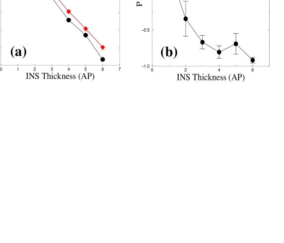
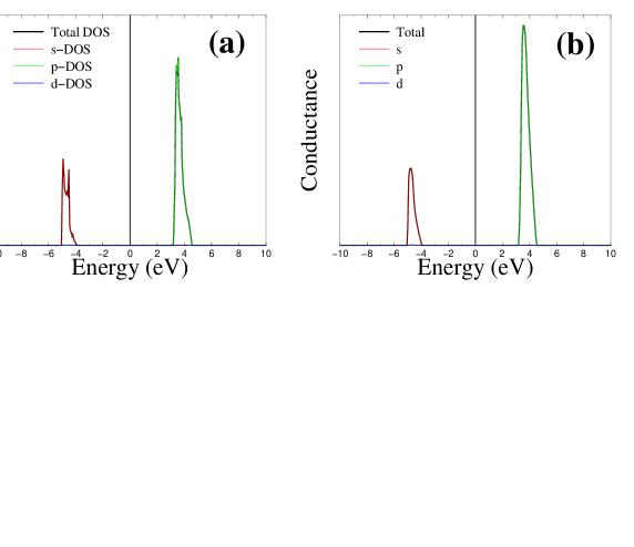
A simple rationale of these effects starts from noting that in Co the spin-polarization of the -electrons at the Fermi energy is positive, while that of the -electrons is negative. Therefore, if the barrier acts selectively on the - and -electrons, different polarizations of the tunneling junction are expected depending on the details of the insulator. Along this line Tsymbal et al. [204] showed that in a Co-based tunneling junction with an -insulator, the polarization is positive if one considers only ss coupling at the interface and becomes negative if sd is also included. Similar calculations based on multi-orbital models have also been presented [206].
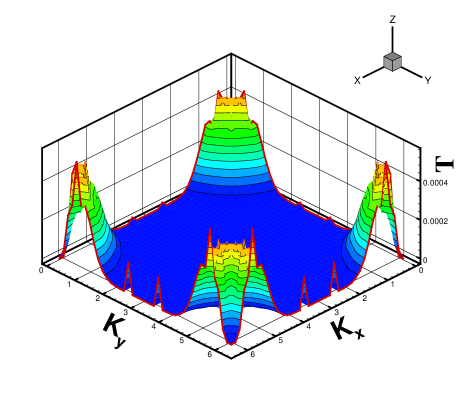
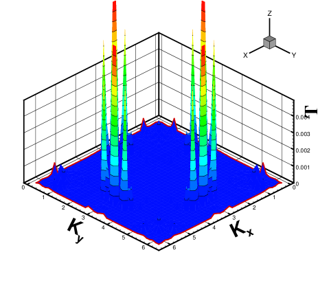
Modern theory of magnetic tunneling junctions is essentially based on the concept of complex band structure [207, 208]. Let us consider a Bloch function in the leads, propagating toward the tunneling barrier. In the “layer” notation used in the previous section this reads
| (5.3) |
where the sum runs over all the possible “layers” forming the lead, is a normalization constant, is the -vector parallel to the transport direction and is a dimensional column vector describing the degrees of freedom of a layer (for an infinite system in the transverse direction ). In the case of a perfectly crystalline system in the direction orthogonal to the transport we can apply the Bloch Theorem in such direction (the - plane in the present notation) and re-write our Bloch function as
| (5.4) |
where the sum runs over all the cells in the two dimensional plane orthogonal to the current, and is now a -dependent -dimensional column vector where is the number of degrees of freedom (orbitals) in the unit cell. Essentially we have reduced the problem of calculating the transport coefficients of the Bloch wave (5.3) to the problem of calculating the transmission coefficients for every Fourier component . This means that at the interface between the leads and the insulating barrier each Fourier component can scatter in the possible channels with the same . However since there are no energy states in the insulating region, all the possible scattering channels are closed channels, i.e. is imaginary (). The extension of the band structure to the complex plane in the direction for the insulator is called “complex band structure”.
If we now consider a particular Fourier component the transmission coefficient for an open channel in the left hand-side lead to be transmitted in the channel in the right hand-side lead is simply
| (5.5) |
where is the scattering amplitude from an open channel in the leads to a closed channel in the insulator. Finally the total transmission coefficient for the specific is simply
| (5.6) |
The equation (5.6) essentially shows that the total transmission coefficient for a particular Fourier component is simply given by the sum over all the decay states in the barrier of an exponential term times a prefactor. The exponential decay is solely a property of the insulator while the prefactor takes into account the matching of the wave-function at the interface between the barrier and the leads. For short barrier the current, and therefore the spin polarization of the junction, will depend mostly on the prefactor and therefore on the fine details of the structure. However for large barriers the transmission is completely dominated by the leading term (the one with the slowest decay) among all the allowed .
It is therefore not surprising that both the TMR ratio and the spin-polarization of the junction change when the barrier thickness increases. Moreover since the leading term in the sum of equation (5.6) is in principle different for different , the transmission coefficient will be strongly resonating over . Clearly this argument is strictly valid in the case of perfect translational invariance both in the barrier and in the leads. When this hypothesis is relaxed and scattering between components is allowed the picture changes. In general the effect of lack of translational invariance is that of smearing the Fermi surface of the leads. This essentially means that the total transmission coefficient will be some average of the of equation (5.6). In particular Tsymbal and Pettifor [209] demonstrated with a tight-binding model that, if the barrier is rich of impurities a simple exponential decay of the wave-function governed by the complex band structure of the insulator is not an appropriate. In this situation the electron transport is via hopping between randomly placed trap states in the barrier and the decay of the transmission coefficient with the barrier width is much slower than that suggested by the simple exponential decay of the leading term of equation (5.6). Interestingly in the large disorder limit the polarization of the junction is well described by the Julliere model [210].
5.2.2 Inelastic effects and bias
To date there are several first principles calculations of tunneling conductance of trilayers [202, 203, 204, 205, 211, 212] obtained in the linear response limit. These generally report quite large TMR ratios, often much larger than those found in experiments, and it is therefore important to investigate the main factors leading to a reduction of the TMR.
In broad terms inelastic scattering may reduce the TMR ratio, although differences are expected depending on whether or not the scattering is spin conserving. These effects have been studied by Bratkovsky using a simple free-electron like model [213] and considering scattering either with impurities, phonons or spin-waves. These three sources of scattering all decrease the TMR ratio although they produce different temperature and bias dependence of the junction current and hence of the spin-polarization. In particular spin-waves absorption/emission results in a drastic reduction of the TMR signal even in the presence of half-metallic contacts, for which the simple density of state argument leads to the expectation of an infinite TMR ratio [214, 215]. Unfortunately a fully ab initio theory of inelastic transport in the quantum limit is still missing and I am not aware of any calculation in that direction.
A somehow easier problem is that connected to the study of finite bias. One of the differences between GMR and TMR junctions is that, while the former operate always at very small bias (then in the linear response limit), in the latter usually a bias of the order of 1 Volt is applied across the insulating layer. Experimentally it was observed that a bias voltage across the device can greatly reduce the TMR signal [216] and this was explained in terms impurity scattering at the interface. Clearly an applied bias can change the equilibrium distribution of the inelastic elementary excitations (phonons and spin-waves) and therefore give rise to a general reduction of the TMR signal [213].
Recently Zhang et al. [217] conducted a first principles study of the conductance and the TMR of a Fe/FeO/MgO/Fe tunneling junction under bias. They used a bias-dependent version the KKR method, where a perfect translational invariance of the system is assumed. For this type of trilayer the translational invariance perhaps is not a bad approximation since epitaxial growth of MgO on Fe has been experimentally demonstrated [218]. Their main finding is that although the changes in the electronic structure due to the bias are minimal and the effective capacitance is consistent with the dielectric constant of MgO, the - characteristic is highly non-linear and the TMR ratio increases as a function of bias. This behavior is essentially due to a reduction of the current associated to the minority spin and in the antiparallel alignment as the bias is applied, and it is explained as a suppression of the resonant contribution to the transmission coefficient coming from surface states. These results, which are expected to be rather general, are in stark contradiction with the experimental data and more investigation in this direction is certainly necessary.
5.3 Domain wall scattering and GMR in atomic point contacts
The typical macroscopic configuration of magnetic materials is that of a collection of regions, the magnetic domains, where the magnetic moments of the individual atoms point in the same direction. In normal conditions the macroscopic magnetization vectors of these regions are randomly aligned in order to minimize the magnetostatic energy. This means that in the interstitial areas between two domains the magnetization vector change direction. It is then natural to ask whether or not these domain walls (DW) bring additional contribution to the electrical resistance. Intuitively one would expect some sort of contribution since the exchange potential depends on the magnetic state.
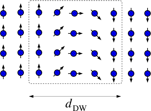
The typical configuration for a domain wall scattering experiment is that presented in figure 33. Essentially the idea is to measure the resistance of a domain wall using a GMR spin-valve experiment, where the non-magnetic spacer is now replaced by the wall itself. The current measured for the configuration of figure 33 is then compared with that obtained for the parallel alignment of the magnetization vectors of the contacts, i.e. when the domain wall is removed. Again the quality factor of the device is given by the GMR ratio defined before.
5.3.1 Infinite domain wall: early theory
The first studies on domain wall scattering were focused on domain walls with infinite cross section. This situation is a good approximation for bulk transition metals, where the magnetic domains can be macroscopic objects. The first calculations on domain wall scattering is due to Cabrera and Falicov [219], who calculated the resistance associated to a domain wall in terms of a tunneling process across the wall. The calculation was carried out for a simple free-electron model and resulted in an exponentially small contribution to the resistance. A few years later Tatara and Fukuyama [220] calculated the contribution of a DW to the resistivity of a magnetic material. They found that in general the presence of a DW enhances the Boltzmann electrical resistivity, and that the DW contribution scales as . However, in situations where the Boltzmann resistivity is small (clean limit at low temperature), the presence of a wall contributes to the decoherence of the electrons, hence decreasing the total electrical resistivity. Therefore the magnetoresistance associated to a domain wall can be either positive or negative, depending on the transport regime encountered.
This last result triggered a considerable interest and several experiments were performed in order to measure the DW resistance. Unfortunately these were often inconclusive and difficult to relate to each other, and both positive [221, 222] and negative magnetoresistance [223, 224] were measured. The main difficulty in these experiments was in separating the tiny change in resistance due to a DW wall from the ordinary contribution of the anisotropic magnetoresistance (AMR).
The reason for the calculated, and indeed measured, small contribution of DW scattering to the resistivity is essentially that the energy associated to the magnetic moment rotation is tiny with respect to the exchange energy. This means that the presence of a DW does not considerably modify the Fermi surface. However early theories were based on simplified descriptions of the electronic structure of the transition metals neglecting the fact that the separation of the bands in the manifold is smaller than the typical exchange. Therefore it becomes increasingly important to study the effect of a DW scattering using realistic bands calculations. The first work of this type was performed by van Hoof et al. using realistic DFT-derived bandstructure and the Landauer formula [225]. In their calculations a local spin rotation was introduced in the direction of the transport, while the system was considered translational invariant in the transverse direction. This reproduces the case of a DW of infinite cross section but finite width. A summary of their results is reported in table 4.
| Property | Fe | Ni | Co |
|---|---|---|---|
| Crystal structure | bcc | fcc | fcc |
| Layer direction | (100) | (100) | (111) |
| (nm) | 40 | 100 | 15 |
| (monolayer) | 276 | 570 | 72 |
| DW-MR | |||
| Bulk DW | -0.39% | -0.16% | -0.46% |
| Abrupt DW | -71% | -58% | -67% |
The main result from this work is that a DW always decreases the electrical conductance, which scales approximately as . As a consequence the MR associated to a bulk DW is always very small, never exceeding 1% in transition metals. These results were later confirmed by other ab initio calculations [226, 227].
Interestingly the original van Hoof’s calculation showed the possibility of remarkably large GMR in the case of abrupt DW (see table 4), which is a domain wall where a 180o degree spin-rotation is achieved in one atomic layer only. For instance in the case of Co DW the GMR ratio is of the same order that the one calculated with similar methods for Co/Cu multilayers [106]. This is not surprising. In fact a majority (minority) electron traveling on the left hand side of the DW, must travel as a minority (majority) on the right hand side. This means that in absence of spin-flip both spin electrons undergo to strong scattering in crossing the DW. Moreover since the bandstructure of the majority band of Co (figure 2) is very similar to that of Cu (figure 3), one expects that the scattering for either spins when crossing a DW is similar to that of the minority electrons in crossing a Co/Cu interface. For this reason it does not appear strange that an abrupt DW presents large GMR. Unfortunately the exchange energy of an abrupt DW is rather large and therefore these are impossible to form in the bulk. A possible way out is to consider very narrow constriction. In this case the energy costs are associated to the rotation of only a small number of magnetic moments, and DW as thick as the constriction lateral dimensions have been predicted [36]. This prediction opened a new avenue to DW GMR and several investigations on the electrical properties of magnetic point contacts began.
5.3.2 Magnetic point contacts and ballistic MR
The experimental situation on DW GMR in magnetic point contact is still controversial. On the one hand there are a number of reports of extremely large GMR [22, 23, 24] reaching up 1,000,000% [228] in either transition metals or other magnetic materials. On the other hand there is an equally long list of works in which either very small [229, 230] or a non-existing GMR was found [231, 232]. The experiments are usually GMR-type of experiments where an external magnetic field is applied to a point contact, and the resistance is recorded. Hence the essential point of controversy is whether or not the large GMR has electronic origin or is just a consequence of the rearrangement of the point contact when the field is applied. Numerous reasons for the mechanical hypothesis have been given including magnetostriction, dipole-dipole interaction between the contact apexes [233] or magnetically induced stress relief [234]. In all these situations the point contact becomes compressed upon the application of a magnetic field, and its cross section increases with a consequent reduction of the two terminal resistance.
In contrast if one wants to follow the electronic-only hypothesis, the fundamental point to bare in mind is that in atomic point contacts the last atom in the constriction is the one that determines the conductance [235, 236]. Hence this cannot exceed the number of valence electrons. Under this assumption we can immediately set an upper bound for the GMR in a point contact made from a strong ferromagnet (Co or Ni). When the magnetization vectors of both sides of the constriction point in the same direction (parallel configuration) the conductance can be as large as 7 , with a contribution of 2 coming from the electrons (both spins contribute) and a contribution of 5 coming from the minority electrons. In this case the majority states are completely filled and they do not contribute to the zero-bias current. In contrast in the antiparallel configuration the conductance of the electrons is blocked and one is left with the 2 contribution from the electrons only. This leads to a GMR ratio of 250%.
Unfortunately this intuitive picture is hardly found in reality, and with the exception of noble metals like gold, the simple one on one mapping of conductance over the number of valence electrons does not hold. The reality is that hybridization mixes the orbital states and usually one has several scattering channels with transmission coefficients smaller than unity. For instance in the case of Co and Ni point contacts conductance histograms with peaks positioned everywhere from to 4 have been reported [237, 238, 239, 240].
To date several calculations on point contact transport through magnetic transition metals have been published. These are all based on the linear response theory of transport using either DFT [241, 242, 243] or tight-binding [244] Hamiltonian. Despite differences due to the details of the methods and the geometrical configuration of the junctions investigated, all these calculations agree on a rather small value of GMR. The common feature is that there are always two channels with -like character (one per spin direction), which are almost perfectly transmitted across the junction. These are quite robust against the contact geometry [242] and clearly do not give rise to any GMR. In contrast the transmission of -type channels is rather sensitive on the details of the junction, although their contribution to the conductance appear to be always smaller than the upper bound of 5 set by the valence. Clearly a precise prediction should take into account the correct experimental configuration of the contact [243], however from this analysis it appears unlikely that a large GMR of purely electronic origin can be found.
A possible additional element to include into this picture is given by the presence of impurities in the point contact. In particular one can speculate that strongly electronegative impurities (for example oxygen) can bind the electrons of the transition metal, therefore eliminating their contributions to the conductance. If this is the case, the conductance will be given by electrons only and one will expect very large GMR ratios. Calculations on these type of systems are particularly problematic since the conventional LSDA (or indeed GGA) to DFT fails in describing the physics of a Mott insulator, which characterizes transition metal mono-oxides such as NiO. A seminal calculation of GMR across an oxygen monolayer sandwiched between (001) Ni electrodes obtained with DFT-LSDA demonstrated a large MR [245]. However the investigation of realistic geometries and of different DFT functionals is still lacking.
5.3.3 Point contacts under bias
In all the theoretical works cited in the previous section the calculations were carried out in the linear response limit. This is appropriate since in actual experiments very small biases are applied in order to prevent the point contact fracture. However in the case of electrodeposited constrictions, in which the typical cross section is much larger than that of single atom contacts, biases in excess of 2 Volt can be applied resulting in interesting diode-like - characteristics [246, 247].
Charging and bias effects in magnetic point contacts were studied recently by Rocha and the present author [248]. For the calculations we used a self-consistent tight-binding model, with two orbitals per atomic site representing respectively the and electrons. In this case the on-site energies present both a Stoner-type term giving rise to the ferromagnetic ground state, and a charging term ensuring local charge neutrality. Finite bias - characteristics were calculated using the NEGF method.
The main result of this calculation is to show that non-symmetric - characteristics can arise from a non-symmetric magnetic configuration of the junction, although the structure itself is perfectly symmetric. In order to demonstrate this concept we model a point contact as a atomic chain comprising four atomic planes and sandwiched between two semi-infinite simple cubic leads with a atom cross section. We investigate two possible situations respectively when the DW is positioned symmetrically or asymmetrically in the junction (see figure 34). The - curves for these two configurations are presented in figure 35, where a clear asymmetry for the asymmetric DW appears.
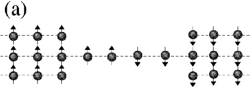
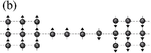
In order to understand this feature we model our magnetic point contact as a magnetic molecule. When the magnetization of the two leads are aligned antiparallel to each other the DW formed inside the molecule splits the HOMO and LUMO states. Hence our system appears as two molecules strongly attached respectively to the left and the right lead, but weakly coupled to each other. This gives rise to the level scheme presented in figure 36a, which is strictly valid only in the case the DW resistance is infinite. Within this scheme the left hand-side part of the PC couples strongly with the left lead therefore presenting a majority spin HOMO and a minority spin LUMO. The situation is opposite on the right hand-side since the magnetization of the right lead is rotated. Recalling the fact that we do not consider the possibility of spin mixing, this configuration presents a large resistance since there are no resonant states with the same spin extending through the entire point contact. If we now apply a bias there will be level shifting. This aligns the majority spins HOMO on the left with the LUMO on the right for positive bias (figure 36b) and the minority LUMO on the left with the HOMO on the right for negative bias (figure 36c).

In addition for positive bias DW charge is accumulated in the first two atomics planes to the left of the DW and it is depleted in the two atomic planes to the right. In the case of a symmetric DW the molecular states to the left and to the right of the Bloch wall charge in a symmetric way with respect to the bias direction. This means that the level alignment responsible for the large current will occur for the same bias difference independently from the bias polarity. In contrast, when the DW is between the third and the fourth plane, more charge can be accumulated (depleted) to the left of the DW with respect to the right, since more states (atomic planes) are available. This means that the alignment of the energy level now depends on the bias polarity, leading to an asymmetric - curve.
The study of magnetic point contact under bias is indeed in its infancy and for a more quantitative analysis ab initio transport methods will be welcome. These probably should include some sort of strong correlation corrections, although perhaps only at the mean field level [149, 150], for describing the ferromagnetism in such reduced dimensions. Moreover we believe that the study of the interplay between magnetic and mechanical effects will be crucial for understanding issues connected with the stability of the contacts and of their magnetic state.
5.4 Spin-transport through carbon nanotubes and nanowires
As I have anticipated in the introduction recently there was a considerable effort in combining the field of molecular- and spin-electronics. The typical device consists in a spin-valve that uses a molecular object as spacer. Potentially this has several advantages compared to more conventional materials since molecules are free of strong spin-flip scattering mechanisms such as spin-orbit and hyperfine interaction or scattering to magnetic impurities. In this race to organic spin-devices the use of carbon nanotubes occupies an important place.
Carbon nanotubes are almost defect-free graphene sheets rolled up in forming 1D molecules with enormous aspect ratios [249]. Their conducting state (metalicity) depends on their chirality, however in the metallic configuration they are ideal conductors with a remarkably long phase coherent length [250, 251]. An important aspect is that the relevant physics at the Fermi level is entirely dominated by the orbitals, which are radially aligned with respect to the tube axis. These include the bonding properties with other materials and between tubes. Therefore carbon nanotubes appear as an ideal playground for investigating both GMR and TMR through molecules. In fact one can expect that two tubes with different chirality will bond to a magnetic surface in a similar way, allowing us to isolate the effects of the molecule from that of the contacts. Indeed TMR-like transport through carbon nanotubes has been experimentally reported by several groups [19, 252, 253, 254, 255].
Now the fundamental question is: why will one expect a large GMR from a carbon nanotube? In order to answer this question I will use an argument derived by Tersoff [256] and then subsequently refined [257] for explaining the contact resistance of a C nanotube on an ordinary metal. In order to fix the ideas let me consider an armchair nanotube (metallic). Its Fermi surface consists only of two points symmetric with respect to the point (see figure 37). The Fermi wave-vector is then with and the C-C bond distance (=1.42 Å).

Assume now that the Fermi surface of a typical magnetic metal simply consists of two spheres with different radii for the different spins. This oversimplified scenario is that of a free-electron model with internal exchange field
| (5.7) |
with () for majority (minority) spins and the exchange energy. The spin-dependent Fermi wave-vectors are then respectively and .
The transport through an interface between such a magnetic metal and the nanotube is determined by the overlap between the corresponding Fermi surfaces. Three possible scenarios are possible. First the Fermi-wave vector of the carbon nanotube is smaller than both and (see figure 37a). In this case in the magnetic metal there is always a -vector that matches the Fermi-wave vector of the nanotube for both spins. Therefore both spins can be injected into the tube and the total resistance will be small and spin-independent.
Secondly the Fermi-wave vector of the carbon nanotube is larger than both and (see figure 37b). In this case there are no available states in the metallic contact whose wave-vectors match exactly the Fermi wave-vector of the carbon nanotube. Therefore in the zero-bias zero-temperature limit the resistance is infinite. Nevertheless as one increases the temperature, phonon assisted transport starts to be possible. Spin electrons can be scattered out of the Fermi surface into states with large longitudinal momentum. At temperature the fraction of electrons with energy above is simply proportional to the Fermi distribution function. However, because of the exchange energy, spin-up electrons will possess higher momentum than spin-down. Therefore one can find more spin-up states with a longitudinal momentum matching the one of the nanotube than spin-down states. This gives a temperature-induced spin-dependent resistance. Hence one should expect that the increase of the temperature will decrease the resistance for spin-up electrons, leaving unchanged that of spin-down electrons.
Finally if the Fermi wave-vector of the carbon nanotube is larger than but smaller than (see figure 37c), only the majority electrons can enter the nanotube and the system becomes fully spin-polarized. In this situation a spin-valve structure made by magnetic contacts and carbon nanotube as spacer is predicted to show an infinite GMR at zero temperature, similar to the case of the half-metals [60]. The increase of the temperature will produce a degradation of the polarization because also the spin-down electrons may occupy high energy states with large longitudinal momentum. Both the spins can be injected and the spin-polarization will depend on the number of occupied states with longitudinal momentum matching the one of the nanotube.
Two important aspects must be pointed out. First all these considerations are based on the assumption of perfectly crystalline systems. This may not be true in reality and the effects of breaking the translational invariance must be considered. From a qualitative point of view disorder will smear the Fermi surface and eventually produce some states with large longitudinal momentum. This will improve the conductance through the nanotube, even if its spin-polarization will be in general dependent on the nature of disorder.
Second, in contacts made from transition metals the simple parabolic band model introduced here is largely non-realistic. The Fermi surface of magnetic metal can comprise different manifolds with different orbital components and the degree of polarization of a junction depends upon how the different manifolds couple to the nanotube. In this case simple theories are only speculative and more realistic bandstructure calculations are needed. These are rather problematic since the problem include the need of describing transition metal leads and a molecule comprising a large number of degrees of freedom.
For this reason most of the calculations to date have used simple tight-binding models without self-consistent procedures [258, 259, 260]. These roughly agree on the possibility of large GMR ratios in transition metals contacted nanotubes, although the actual values predicted are somehow affected by the different methods and the contact geometry. In addition more sophisticated calculations based on DFT and non-equilibrium Green’s function method for simpler carbon chains have been reported [261, 262]. These give interesting insights into the spin transport properties through organic materials although they fail in providing a realistic description of magnetic transition metal contacts. In the case of reference [261] the contacts are made from Al leads in which a strong magnetic field is applied, while in the case of reference [262] the contacts are Au wires and the spin polarization is obtained by inserting a Co atoms between the C chains and the electrodes.
5.5 Molecular devices
Together with their indisputable spectacular properties carbon nanotubes as building blocks in nanoscale devices have an important drawback, namely their saturated orbitals make the bonding with electrodes problematic. This is not only structurally weak but also inefficient at transmitting electrons. For this reason molecules other than nanotubes look more appealing for constructing electronic and therefore spin- devices. Molecules offer an almost infinite range of HOMO-LUMO gaps and molecular orbital types, and they can be functionalized in several ways in order to attach them to metallic contacts. Therefore they appear as the ultimate systems for engineering spin-devices.
Recently there have been several investigations of transport in molecular spin-valve like devices. These include hot electron coherent spin transfer across molecular bridges [26], spin-injection in -conjugated molecules [21, 25] and organic tunneling junctions [263]. All these demonstrate convincingly the possibility of performing spin-physics in organic compounds, although problems connected with a generally poor reproducibility still need to be addressed.
The modeling of such devices is even more challenging than that involving nanotubes since large biases can be applied and an accurate description of the electrostatic is also needed. This adds up to the already discussed difficulty of describing magnetic transition metal leads, and makes the problem a tough theoretical challenge. A few seminal studies on transport through 1,4-benzene-dithiolate molecular spin-valves [264, 265] have appeared. However they either overlook the electrostatic problem [265], or the leads are non-magnetic and the spin-polarization is obtained by a magnetic cluster added at the top of Au electrodes [264].
To the best of my knowledge the code Smeagol [100] is the only one to date able of calculating accurate - characteristics of devices employing magnetic leads. Here I briefly summarize the spin-transport properties of spin-valve made from Ni leads and a molecule as spacer [101]. As an example I will analyze two different molecules, respectively [8]-alkane-dithiolate (octane-dithiolate) and 1,4-[3]-phenyl-dithiolate (tricene-dithiolate). A schematic density of states and the charge density isosurfaces of the HOMO and LUMO states for the isolated molecules are presented in figures 38 and 39.
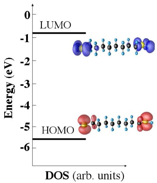
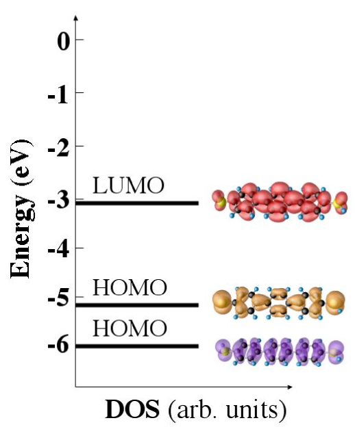
The two molecules present two fundamental differences. First the HOMO-LUMO gap (this is the DFT-LDA gap, which might be substantially smaller than the actual gap) in octane (5 eV) is about twice as big as the one of tricene (2.5 eV). Secondly in octane the charge density of both the HOMO and the LUMO states has predominant amplitude around the S atoms of the thiol group, with little density on the central carbon backbone. In contrast the HOMO and LUMO states of tricene are delocalized throughout the whole molecule with charge density concentrated both on the end-groups and on the central phenyl groups. This leads us to expect that the octane and the tricene will form respectively TMR and GMR devices, as actually found in our calculations [101].
In the case of the 1,4-[n]-phenyl-dithiolate we find that the current does not scale sensibly with the number of phenyl groups in the molecule and the transport is essentially resonant through a molecular state. This picture is enforced by the fact that the zero-bias transmission coefficient approach unity for energies close to the leads Fermi level. In addition from the study of the evolution of the orbital resolved density of states as a function of the distance between the thiol group and the electrodes we identify such a resonant state as the HOMO state of tricene. However it is worth mention that this appears rather broad and spin-splitted, because of the strong coupling with the orbitals of the leads [101]. Therefore the Ni/tricene/Ni spin-valve behaves as an all-metal spin-valve.
In contrast the zero-bias transmission coefficient of the Ni/octane/Ni junction presents a sharp peak at that scales exponentially with the number of alkane groups (). This clearly demonstrates that the device is in a tunneling regime. It is interesting to note that such an exponent is similar to that found for the same molecules attached to gold (111) surfaces [266]. Also in this case the coupling between the thiol groups and the electrodes is strongly, however because of the highly localized nature of the HOMO and LUMO states, there in not a molecular state extending through the entire structure close to the Fermi level. Hence the Ni/octane/Ni junction has the features of a TMR spin-valve.
In both cases the the spin-transport properties can be qualitatively understood in terms of transport through a single molecular state (see figure 40). Let be the majority spin hopping integral from one of the leads to the molecular state, and the same quantity for the minority spins. Then neglecting multiple scattering from the contacts, the total transmission coefficients of the entire spin-valve in the parallel state can be written and respectively for the majority and minority spins. Similarly the transmission in the anti-parallel configuration is . Thus is a convolution of the transmission coefficients for the parallel case .
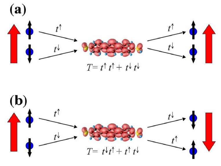
This qualitative argument gives us a tool for understanding the MR. For the case in which only one spin couples to the molecular state, the total transmission in the antiparallel case will be identically zero since either or vanishes. This is the most desirable situation in real devices since, in principle, an infinite can be obtained. Furthermore if for a particular energy window the transport is through two distinct molecular states, which are respectively coupled to the majority and minority spin only, then in this window one will find , but .
The - characteristics of both the molecules are strongly non-linear with the bias and consequently also the GMR ratio suffers this non-linearity. In table 5 I present a summary of our results, including the maximum and the minimum of the GMR ratio over the bias range studied ( Volt) and the device resistance at 1 Volt for the parallel configuration of the leads. These clearly demonstrate that molecular spin valves can yield large MR ratios. In the case of TMR junction (octane) both the resistance and the TMR ratio are in the same range as in recent experiments on octane-based Ni spin-valves [263]. However a direct comparison is difficult since the actual number of molecules bridging the two electrodes is not known with precision, and a degradation of the GMR signal due to spin-flip and electron-phonon scattering, misalignment of the magnetization of the contacts and current shortcut through highly conductive pin-holes, can drastically reduce .
| Device | GMRmax (%) | GMRmin (%) | () |
|---|---|---|---|
| Ni/S-octane-S/Ni | 110 | 30 | 5.9106 |
| Ni/S-tricene-S/Ni | 660 | 51 | 8.2104 |
| Ni/Se-tricene-Se/Ni | 865 | 82 | 1.2105 |
| Ni/Te-tricene-Te/Ni | 870 | 124 | 2105 |
In contrast in the case of metallic (tricene) junctions the GMR ratio can reach very high values exceeding a few hundreds percent. In addition in the table I have reported results for the same triacene molecule, where now the anchoring groups are Se and Te atoms. Since S, Se and Te belong to the same chemical group in the periodic table they present a similar chemistry, and the main difference is simply a larger separation between such a group and the Ni contacts. This in fact increases with the atomic number of the anchor. Such an increase reduces the overlap between the molecule and the electrodes and enhances the device resistance. However since this change in resistance depends on the spin direction, being more pronounced for the minority spins, we find a general increase of the GMR maximum when going from S to Se to Te. These findings have the important consequence that the GMR signal can be tuned by an appropriate choice of the anchoring chemistry.
The field of molecular- spin-electronics is certainly in its early infancy, although it has already demonstrated part of its potential. Clearly more investigations are needed both theoretical and experimental, in particular addressing the problems of stability, efficiency and device production yield. However the future looks very promising, in particular since novel phenomena such as molecular spin rectification or spin inversion can be demonstrated.
5.6 Magnetic proximity
I wish to close this section with a brief discussion of a recently discovered phenomenon, which is only indirectly connected to spin-transport, but that may open a novel avenue to spin-manipulation at the nanoscale. This is the magnetic proximity effect. The basic idea is quite simple: there is always some charge transfer at the contact between a conducting molecule and a metal associated with the alignment of their respective chemical potentials. In a ferromagnet, the densities of states for spin up and spin down electrons at the Fermi level are different. Therefore one expects some degree of spin transfer to accompany the charge transfer. Roughly speaking, the transferred electrons are more abundant for one of the two spin directions leading to a spin imbalance in the electron transfer that accounts for a contact-induced magnetic moment on the molecule. In the limit of a half metal, where either the majority or minority electrons are absent at the Fermi level, the spin transfer is equal to the charge transfer.
A first indirect evidence of this effect was found recently by the group of J.M.D. Coey, who investigated the magnetic state of a carbon meteorite, and concluded that some unaccounted magnetization could be attributed to a tiny moment of the carbon atoms induced by the proximity with magnetic impurities [267]. Subsequently Ferreira and Sanvito derived a close system of equations for the induced magnetic moment and for the energetic of a carbon nanotube on a magnetic surface [268]. The calculation was based on a simple tight-binding model with a reasonable choice of parameters for the coupling between the nanotube and a cobalt surface. The calculations revealed that induced magnetic moments of the order of 0.1 per carbon atom in contact with the surface can be achieved at room temperature. This paved the way for a more controlled set of experiments in order to demonstrate the magnetic proximity effect.
Experimentally the problem is to detect such a small spin transfer against the huge background coming from the ferromagnetic substrate. One possible strategy is to chose a smooth thin metal film as a substrate and look for the stray field around the nanotube. A uniformly magnetized thin film creates no stray field whatever its direction of magnetization. In contrast a magnetized nanotube will produce a stray field, which will be directly detectable. This was the basic idea behind the experiments from Céspedes et al. [20], who measured induced magnetic moments in excess of 0.1 per carbon atom in contact, in good agreement with the theoretical prediction. The experiment consists in taking AFM and MFM images of nanotubes on various surfaces. The difference between the topographic (AFM) and the magnetic images (MFM) is a direct measure of the stray field coming from the nanotube and therefore provides evidence for the induced magnetic moment.
In figure 41 and 42 I show the typical AFM and MFM pictures for nanotubes respectively on non-magnetic and magnetic substrates. When the substrate is not magnetic the MFM-AFM image does not show the presence of the tube, which indicates that this latter does not produce any stray field. In contrast the same picture for a nanotube on magnetite (see figure 42) unambiguously shows contrast and demonstrates the presence of an induced magnetic moment with a clear magnetic domain pattern.
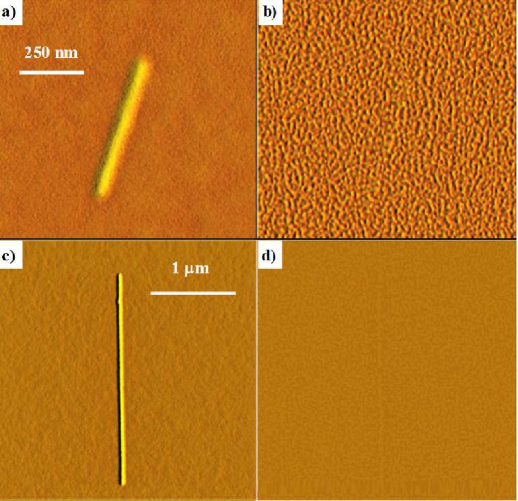
In the another experiment, Mertins et al. [269] produced a multilayer of thin, alternating iron and carbon layers, of thickness 2.55 and 0.55 nm, respectively. Then, they probed locally the magnetic moment of the carbon by X-ray magneto-optical reflectivity of polarized synchrotron radiation. In this type of measurement the Fe and C absorption edges differ by about 500 eV enabling one of establishing with precision whether the magnetic moment comes from C or not. With this method magnetic moment of the order of 0.05 were found.
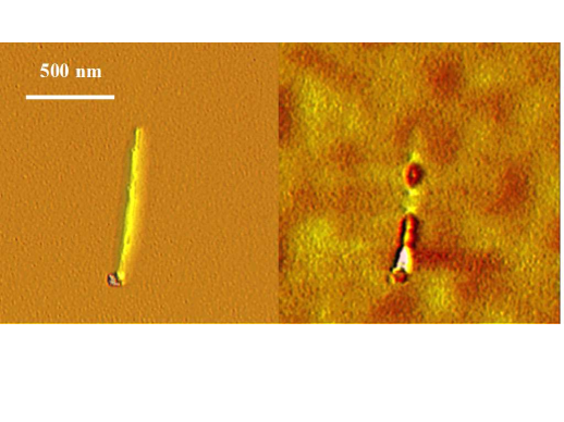
It is important to point out that the magnetic proximity effect does not imply intrinsic ferromagnetism [270] and no spin aligning potential exists in carbon. This means that a magnetic moment is detected only when a second ferromagnetic material is present and when good contact is made. However this effect may have important applications in spintronics. For instance one can envision four terminal devices, where two non-magnetic contacts are used for charge injection while two other magnetic electrodes are used for the spin-manipulation. These types of set-up clearly add a novel dimension to spintronics and perhaps will help in overcoming the spin-injection problem.
6. Conclusion
A decade after the discovery of the GMR effect the future of spin-electronics in nanoscale systems looks bright. This is mainly due to the improved understanding of the spin-transport mechanisms and the better control over the device processing. At the same time the possibility of conducting spin-transport measurements in systems comprising a handful of atoms has opened completely new prospectives. We can envision in a near future new devices where the spin and molecular functionalities will be combined achieving a broad range of applications, from biological sensors to tools for coherent quantum data processing.
From the theoretical side the last decade has also witnessed a rapid evolution of computational methods for both electronic structure and quantum transport. Several numerical implementations are currently available. The most advanced of them are based on ab initio schemes and therefore do not depend on parameters obtained from experiments. These open the way to a physics “without compromises”, where the numerical predictions must reproduce the experimental data, if the systems under investigation are the same. For this reason ab initio transport schemes have became an invaluable tools.
In this review I have discussed the two main philosophies behind quantum transport, namely the scattering theory and the non-equilibrium Green function method. Then I have overviewed the numerical tools available to date and I have reviewed the main successes of quantitative transport theory applied to spin problems. These include the GMR and TMR effects, spin transport through atomic point contacts and through organic molecules. I deliberately have not addressed problems connected with inelastic effects both of mechanical and magnetic origin, and with the need for more accurate and flexible electronic structure methods. Here the field is rather vast and in continuous evolution and it deserves a review on its own. Certainly the future of modeling spin transport at the nanoscale is dawning.
7. Acknowledgment
This work is supported by Science Foundation of Ireland under the grant SFI02/IN1/I175. It is my privilege to thank Alexander Reily Rocha, Cormac Toher, Maria Tsoneva and Nicola Jean for careful reading the manuscript and Colin Lambert, Jaime Ferrer, Michael Coey, Nicola Spaldin, John Jefferson, Alessio Filippetti, Tchadvar Todorov and Kieron Burke for useful discussions.
A Retarded Green function for a double infinite system
In this appendix I present the explicit calculation leading to the equation (3.75) for the Green’s function of a double infinite system. The starting point is the equation (3.73)
| (A.1) |
with and two vectors to be determined. The expression of equation (A.1) to be a Green function must be continuous for and must satisfy the Green equation
| (A.2) |
The first condition yields immediately to the relation
| (A.3) |
while the second gives
| (A.4) |
The task is now to re-write the vectors ’s as a function of the known vectors ’s and their dual ’s. First note that by adding and subtracting to the (A.4) the expression
| (A.5) |
it is possible to re-write the (A.4) in the following compact form
| (A.6) |
where the definition of of equation (3.68) has been used. Now consider the continuity equation (A.3) and multiply the left-hand side by the dual vector and the right-hand side by . It yields respectively to two expressions that relate to
| (A.7) |
| (A.8) |
If now one substitutes the equations (A.7) and (A.8) into the equation (A.6) and uses the continuity equation (A.3), the following fundamental relation is obtained
| (A.9) |
from which it follows immediately
| (A.10) |
In the second equality of the equation (A.10) I have used the continuity equation (A.3). Note that the equation (A.10) expresses explicitly the vectors ’s in term of the known quantities , and . Therefore ’s may be computed by simply multiplying the (A.10) for the correct dual vectors. By doing so I obtain
| (A.11) |
B General current operator and rotation in the degenerate space
I this appendix I will generalized the current operator introduced in section 3.2.1 and discuss the rotation needed to diagonalize it in the case in which the vectors ’s are degenerate. Let us start by considering the current matrix at the position . It can be easily expressed as the time derivative of the density matrix at the same point
| (B.1) |
where are the coefficients of the time-dependent wave-function at the position satisfying the time-dependent Schrödinger equation
| (B.2) |
By explicitly evaluating the time derivative in equation (B.1), and by using the Schrödinger equation and its complex conjugate, the current matrix can be written in the following transparent form
| (B.3) |
where , and are defined respectively as
| (B.4) |
| (B.5) |
| (B.6) |
In the calculation of the relations above I simplified the time-dependent component of the wave-function and expressed the current matrix by mean of the column vectors introduced in section 3.3.4 through the time-independent Schrödinger equation (3.66). Note that does depend only on the value of the wave-function at the position , while and depend also respectively on its value at the position and . Note also that the expressions (B.5) and (B.6) are formally identical to their one-dimensional counterparts (3.14) and (3.15) once the on-site energy and the hopping integral are replaced respectively by the intra- and inter-slice matrices and .
Now evaluate the expectation value of the current by taking the trace of the current matrix. It is easy to show that
| (B.7) |
with
| (B.8) |
| (B.9) |
In the calculation of the equations (B.8) and (B.9) I used the circular property of the trace . Note that the expectation value of vanishes. As in the one dimensional case the relations (B.8) and (B.9) have a clear interpretation. and represent the current matrices for electrons propagating respectively to the left (left-moving) and to the right (right-moving). Note that in the case of a translational-invariant system can be written in the Bloch form of equation (3.67)
| (B.10) |
If now one substitutes the (B.10) into the (B.8-B.9) it is easy to show that as expected from the translational invariance. Moreover note again that local current conservation is achieved at the length scale of a single slice, i.e. by taking the trace of the matrices . This is equivalent to sum up all the orbital currents of the cell.
The final part of this appendix is dedicated to show that the states of the form diagonalize the current. As anticipated in section 3.3.4 this is not strictly valid in the case of different corresponding to the same . Nevertheless in such a case I will show that there is always a rotation in the degenerate space that diagonalizes the current.
Consider for instance the right-moving current (all the following arguments can be applied to the left-moving counterpart), and a Bloch state
| (B.11) |
and calculate the expectation value of the current for such a state. It easy to show that this yields to the equation
| (B.12) |
If one now assumes that the off-diagonal matrix elements vanish (’s diagonalize the current), then the states (B.11) diagonalize the current and curry unitary flux if the normalization constant is taken to be
| (B.13) |
with defining the group velocity. Note that the states (B.11) with the normalization constant (B.13) are the ones introduced in section 3.3.4, which guarantee the unitarity of the matrix.
The final step is to demonstrate that diagonalizes the current. To achieve this, consider the Schrödinger equation evaluated on such a Bloch state and its complex conjugate
| (B.14) |
| (B.15) |
By multiplying the first equation by to the left and the second by to the right one obtains the relation
| (B.16) |
The (B.16) is identically satisfied if , also if . This occurs when one or more wave-vectors are degenerate (ie there are many ’s for the same ). In the case this does not happen few algebraic manipulations yield to the relation
| (B.17) |
The last equality shows the cancellation of the off-diagonal terms in the expression of the expectation value of the right-going current (B.12). This means that in the case in which there is no degeneracy in , the states diagonalize the current. Nevertheless in the case in which degeneracy is present one can perform a unitary rotation in the degenerate space and construct a new basis in which the current is diagonal. To show explicitly how to obtain this rotation consider a set of vectors corresponding to the same wave vector and construct the “reduced” current matrix, whose matrix elements are
| (B.18) |
Since the “reduced current” is an hermitian matrix. Therefore it has always a diagonal form. Moreover the transformation matrix which diagonalizes , is a unitary matrix. If is the diagonal form of I can write such a unitary transformation as
| (B.19) |
It follows that the transformation also transforms the basis into a “rotated” basis which diagonalize the current (note that the “reduced current” is simply the total current introduced above calculated onto a subset of the total Hilbert Space). By evaluating the equation (B.19) the explicit definition of is obtained
| (B.20) |
The equation (B.20) completes the demonstration.
C Green function-Wave function projector
In this appendix I will show that the projector that maps the RGF for the double infinite system on the corresponding wave-function projects also the total RGF (system = scatterer + leads) on the corresponding total-wave function. Consider the total Hamiltonian
| (C.1) |
where describes the leads and describes the scattering region. The Schrödinger equation and the Green equation for the leads (without any scattering region) are respectively
| (C.2) |
| (C.3) |
with the Green function, the energy and the identity matrix. The corresponding equations for the whole system (scatterer + leads) are
| (C.4) |
| (C.5) |
Furthermore , and , are related by the respective Dyson’s equations
| (C.6) |
| (C.7) |
Define now the projector in such a way that
| (C.8) |
If one now uses the Dyson equation for (C.6) together with the definition of , it follows immediately
| (C.9) |
where I used the Dyson equation for (C.7). The equation (C.9) completes the demonstration and shows that also maps onto .
References
- [1] J. L. Simonds, Physics Today 48, 26 (1995).
- [2] M. N. Baibich et al., Phys. Rev. Lett. 61, 2472 (1988).
- [3] G. Binasch, P. Grünberg, F. Saurenbach, and W. Zinn, Phys. Rev. B 39, 4828 (1989).
- [4] P. Bruno, Phys. Rev. B 52, 411 (1995).
- [5] H. Ohno, Science 281, 951 (1998).
- [6] H. Ohno, J. Magn. Magn. Mater 200, 110 (1999).
- [7] J. M. Kikkawa and D. D. Awschalom, Phys. Rev. Lett. 80, 4113 (1998).
- [8] J. M. Kikkawa and D. D. Awschalom, Nature 397, 139 (1999).
- [9] I. Malajovich, J. M. Kikkawa, D. D. Awschalom, J. J. Berry, and N. Samarth, Phys. Rev. Lett. 84, 1015 (2000).
- [10] M. Poggio et al., Phys. Rev. Lett. 91, 207602 (207602).
- [11] S. A. Wolf et al., Science 294, 1488 (2001).
- [12] G. Prinz, Science 282, 1660 (1998).
- [13] G. Prinz, Phys. Today 48, 58 (1995).
- [14] D. P. D. Vincenzo, Science 270, 255 (1995).
- [15] C. Joachim, J. K. Gimzewski, and A. Aviram, Nature (London) 408, 541 (2000).
- [16] S. J. Tans, A. R. M. Verschueren, and C. Dekker, Nature 393, 49 (1998).
- [17] J. Chen, M. A. Reed, A. M. Rawlett, and J. M. Tour, Science 286, 1550 (1999).
- [18] Z. Yao, H. W. C. Postman, L. Balents, and C. Dekker, Nature 402, 273 (1999).
- [19] K. Tsukagoshi, B. W. Alphenaar, and H. Ago, Nature 401, 572 (1999).
- [20] O. Céspedes, M. S. Ferreira, S. Sanvito, M. Kociak, and J. M. D. Coey, J.Phys.: Condens Matter 16, L155 (2004).
- [21] Z. H. Xiong, D. Wu, Z. V. Vardeny, and J. Shi, Nature 427, 821 (2004).
- [22] N. García, M. Muñoz, and Y. W. Zhao, Phys. Rev. Lett. 82, 2923 (1999).
- [23] S. Z. Hua and H. D. Chopra, Phys. Rev. B, Rapid Communications 67, 060401 (2003).
- [24] J. J. Versluijs, M. A. Bari, and J. M. D. Coey, Phys. Rev. Lett. 87, 026601 (2001).
- [25] V. Dediu, M. Murgia, F. C. Matacotta, C. Taliani, and S. Barbanera, Solid State Communication 122, 181 (2002).
- [26] M. Ouyang and D. D. Awschalom, Science 301, 1074 (2003).
- [27] T. Valet and A. Fert, Phys. Rev. B 48, 7099 (1993).
- [28] L. H. Thomas, Proc. Cambridge Phil. Soc. 23, 542 (1927).
- [29] E. Fermi, Z. Physik 48, 73 (1928).
- [30] N. D. Ashcroft and N. D. Mermin, Solid State Physics, Int. Thompson Pub., 1976.
- [31] D. G. Pettifor, Bonding and structure of molecules and solids, Oxford University Press, Oxford, UK, 2002.
- [32] M. A. Ruderman and C. Kittel, Phys. Rev. 96, 99 (1954).
- [33] T. Kasuya, Prog. Theor. Phys. 16, 58 (1956).
- [34] K. Yoshida, Phys. Rev. 106, 893 (1957).
- [35] N. A. Spaldin, Magnetic Materials: Fundamentals and device applications, Cambridge University Press, Cambridge, UK, 2003.
- [36] P. Bruno, Phys. Rev. Lett. 83, 2425 (1999).
- [37] B. Kramer and A. MacKinnon, Rep. Prog. Phys. 56, 1469 (1993).
- [38] D. Bozec et al., Phys. Rev. Lett. 85, 1314 (2000).
- [39] N. Mott, Proc. Roy. Soc. A 153, 699 (1936).
- [40] W. C. Chiang, Q. Yang, W. P. P. Jr., R. Loloee, and J. Bass, J. Appl. Phys. 81, 4570 (1997).
- [41] S. Steenwyk, S. Y. Hsu, R. Loloee, J. Bass, and W. P. P. Jr., J. Mag. Mag. Mater. 170, L1 (1997).
- [42] P. Delaney and J. Greer, Phys. Rev. Lett. 93, 036805 (2004).
- [43] S. N. Yalirakia, A. E. Roitberg, C. Gonzalez, V. Mujica, and M. A. Ratner, J. Chem. Phys. 111, 6997 (1999).
- [44] H. Hohenberg and W. Kohn, Phys. Rev. 136, B864 (1964).
- [45] W. Kohn and L. Sham, Phys. Rev. 140, A1133 (1965).
- [46] P. Ordejón, Comp. Mat. Sci. 12, 157 (1998).
- [47] M. A. L. Marques and E. K. U. Gross, Time-Dependent Density Functional Theory, in Lecture Notes in Physics: Vol 620, Springer-Verlag, Heidelberg, 2003.
- [48] E. Runge and E. K. U. Gross, Phys. Rev. Lett. 52, 997 (1984).
- [49] R. Baer, T. Seideman, S. Ilani, and D. Neuhauser, J. Chem. Phys. 120, 3387 (2004).
- [50] R. Gebauer and R. Car, Phys. Rev. B 70, 125324 (2004).
- [51] A. P. Sutton, Electronic Structure of Materials, Oxford University Press, Oxford, UK, 1996.
- [52] M. Elstner et al., Phys. Rev. B 58, 7260 (1998).
- [53] A. P. Horsfield and A. M. Bratkovsky, J. Phys.: Condens. Matter 12, R1 (2000).
- [54] T. N. Todorov, J. Phys.: Cond. Matter 14, 3049 (2002).
- [55] S. Sanvito, J. H. Jefferson, and C. J. Lambert, Phys. Rev. B 60, 7385 (1999).
- [56] G. A. Gehring, An introduction to the theory of normal and ferromagnetic materials, in “Spin electronics” Lecture Notes in Physics: Vol 569, Springer-Verlag, Heidelberg, 2001.
- [57] J. M. Soler et al., J. Phys. Cond. Matter 14, 2745 (2002).
- [58] T.-S. Choy, Ph.D. Thesis, University of Florida (2001) , http://www.phys.ufl.edu/fermisurface/.
- [59] J. C. Slater and G. F. Koster, Phys. Rev. 94, 1498 (1954).
- [60] J. M. D. Coey and S. Sanvito, J. Phys.: Appl. Phys. 37, 988 (2004).
- [61] I. I. Mazin, Phys. Rev. Lett. 83, 1427 (1999).
- [62] P. B. Allen, Phys. Rev. B 17, 3725 (1978).
- [63] S. P. Lewis, P. B. Allen, and T. Sasaki, Phys. Rev. B 55, 10253 (1997).
- [64] B. Nadgorny et al., Phys. Rev. B 63, 184433 (2001).
- [65] D. Singh, Phys. Rev. B 55, 313 (1997).
- [66] R. Landauer, Phil. Mag. 21, 863 (1970).
- [67] R. Landauer, IBM J. Res. Develop. 1, 233 (1957).
- [68] M. Büttiker, Y. Imry, R. Landauer, and S. Pinhas, Phys. Rev. B 31, 6207 (1985).
- [69] Y. V. Sharvin, Zh. Eksp. Teor. Phys. 48, 984 (1965).
- [70] Y. V. Sharvin, Sov. Phys. JETP 21, 655 (1965).
- [71] M. Julliere, Phys. Lett. A 50, 225 (1975).
- [72] E. Y. Tsymbal and D. G. Pettifor, J. Phys.: Condens. Matter 9, L411 (1997).
- [73] A. F. Andreev, Sov. Phys. JETP 19, 1228 (1964).
- [74] R. Meservey and P. M. Tedrow, Phys. Rep. 238, 173 (1994).
- [75] M. J. M. de Jong and C. Beenakker, Phys. Rev. Lett. 74, 1657 (1995).
- [76] F. Taddei, S. Sanvito, and C. J. Lambert, J. Low Temp. Phys. 124, 305 (2001).
- [77] G. Schmidt, D. Ferrand, L. W. Molenkamp, A. T. Filip, and B. J. van Wees, Phys. Rev. B 62, R4790 (2000).
- [78] E. I. Rashba, Eur. Phys. J. B 29, 513 (2002).
- [79] V. Y. Kravchenko and E. I. Rashba, Phys. Rev. B 67, 121310 (2003).
- [80] H. X. Tang, F. G. Monzon, R. Lifshitz, M. C. Cross, and M. L. Roukes, Phys. Rev. B 61, 4437 (2000).
- [81] Y. Ohno et al., Nature 402, 790 (2001).
- [82] R. Fiederling et al., Nature 402, 787 (1999).
- [83] A. M. Bratkovsky, Appl. Phys. Lett. 72, 2334 (1998).
- [84] N. Agraït, A. L. Yeyati, and J. M. van Ruitenbeek, Phys. Rep. 377, 81 (2003).
- [85] A. J. Heeger, S. Kivelson, and J. R. Schrieffer, Rev. Mod. Phys. 60, 782 (1988).
- [86] S. I. Kiselev et al., Nature 425, 380 (2003).
- [87] M. Klaüi et al., Appl. Phys. Lett. 83, 105 (2003).
- [88] L. Berger, J. Appl. Phys. 55, 1954 (1984).
- [89] L. Berger, J. Appl. Phys. 71, 2721 (1992).
- [90] G. Tatara and H. Kohno, Phys. Rev. Lett. 92, 086601 (2004).
- [91] M. D. Ventra, Y.-C. Chen, and T. Todorov, Phys. Rev. Lett. 92, 176803 (2004).
- [92] D. Papaconstantopoulos, Handbook of the Band Structure of Elemental Solids, Plenum, New York, 1986.
- [93] http://cst www.nrl.navy.mil/bind/.
- [94] M. Büttiker, IBM J. Res. Develop. 32, 317 (1988).
- [95] A. Kamenev and W. Kohn, Phys. Rev. B 63, 155304 (2001).
- [96] N. D. Lang, Phys. Rev. B 36, 8173 (1987).
- [97] E. Economou, Green’s Functions in Quantum Physics, Springer-Verlag, New York, 1983.
- [98] D. Lee and J. D. Joannopoulos, Phys. Rev. B 23, 4988 (1981).
- [99] D. Lee and J. D. Joannopoulos, Phys. Rev. B 23, 4997 (1981).
- [100] A. R. Rocha et al., in preparation , http://www.smeagol.tcd.ie.
- [101] A. R. Rocha et al., Nature Materials 4, 335 (2005). http://www.nature.com/nmat/journal/vaop/ncurrent/abs/nmat1349.html.
- [102] S. Sanvito, C. J. Lambert, J. H. Jefferson, and A. M. Bratkovsky, Phys. Rev. B 59, 11936 (1999).
- [103] C. Lambert, V. Hui, and S. Robinson, J. Phys.: Condens. Matter 5, 4187 (1993).
- [104] G. Wexler, Proc. Phys. Soc. 89, 927 (1966).
- [105] G. E. W. Bauer, A. Brataas, K. M. Schep, and P. J. Kelly, J. Appl. Phys. 75, 6704 (1994).
- [106] K. M. Schep, P. J. Kelly, and G. E. W. Bauer, Phys. Rev. Lett. 74, 586 (1995).
- [107] K. M. Schep, P. J. Kelly, and G. E. W. Bauer, Phys. Rev. B 57, 8907 (1998).
- [108] S. Sanvito and N. A. Hill, Phys. Rev. Lett. 87, 267202 (2001).
- [109] S. Sanvito, Phys. Rev. B 68, 054425 (2003).
- [110] M. P. Lopez-Sancho, J. M. Lopez-Sancho, and J. Rubio, J. Phys. F 14, 1205 (1984).
- [111] M. P. Lopez-Sancho, J. M. Lopez-Sancho, and J. Rubio, J. Phys. F 15, 851 (1985).
- [112] M. B. Nardelli, Phys. Rev. B 60, 7828 (1999).
- [113] J. Mathon, J. Phys. Condens. Matter 1, 2505 (1989).
- [114] J. Mathon, Phys. Rev. B 55, 960 (1997).
- [115] J. Korringa, Physics 13, 392 (1947).
- [116] W. Kohn and N. Rostoker, Phys. Rev. 94, 1111 (1954).
- [117] J. M. MacLaren, S. Crampin, D. D. Vvedensky, and J. B. Pendry, Phys. Rev. B 40, 12164 (1989).
- [118] J. M. MacLaren, X. G. Zhang, W. H. Butler, and X. Wang, Phys. Rev. B 59, 5470 (1999).
- [119] W. Wildberger, R. Zeller, and P. H. Dederichs, Phys. Rev. B 55, 10074 (1997).
- [120] P. Mavropoulos, N. Papanikolaou, and P. H. Dederichs, Phys. Rev. B 69, 125104 (2004).
- [121] R. Kubo, J. Phys. Soc. Jpn. 12, 570 (1957).
- [122] A. Calzolari, N. Marzari, I. Souza, and M. B. Nardelli, Phys. Rev. B 69, 035108 (2004).
- [123] N. Marzari and D. Vanderbilt, Phys. Rev. B 56, 12847 (1997).
- [124] A. Ramšak and T. Rejec, cond-mat/0310452 .
- [125] T. Rejec and A. Ramšak, Phys. Rev. B 68, 035342 (2003).
- [126] T. Rejec and A. Ramšak, Phys. Rev. B 68, 033306 (2003).
- [127] K. Burke, R. Gaudoin, and F. Evers, preprint .
- [128] K. Burke, R. Car, and R. Gebauer, cond-mat/0410352 .
- [129] S. K. Upadhyay, A. Palanisami, R. N. Louie, and R. A. Buhrman, Phys. Rev. Lett. 81, 3247 (1998).
- [130] S. K. Upadhyay, R. N. Louie, and R. A. Buhrman, Appl. Phys. Lett. 74, 3881 (1999).
- [131] R. J. Soulen et al., Science 282, 85 (1998).
- [132] P. G. de Gennes, Superconductivity of Metals and Alloys, Addison-Wesley, New York, 1989.
- [133] C. J. Lambert and R. Raimondi, J. Phys.: Condens. Matter 10, 901 (1998).
- [134] C. Caroli, R. Combescot, P. Nozieres, and D. Saint-James, J. Phys. C: Solid State Phys. 5, 21 (1972).
- [135] J. Ferrer, A. Martín-Rodero, and F. Flores, Phys. Rev. B 38, 10113 (1988).
- [136] S. Datta, Electronic Transport in Mesoscopic Systems, Cambridge University Press, Cambridge, UK, 1995.
- [137] H. Haug and A. P. Jauho, Quantum Kinetics in Transport and Optics of Semiconductors, Springer, Berlin, 1996.
- [138] Y. Xue, S. Datta, and M. A. Ratner, Chem. Phys. 281, 151 (2002).
- [139] S. Datta, Nanotechnology 15, S433 (2004).
- [140] J. Janak and A. Williams, Phys. Rev. B 14, 4199 (1976).
- [141] C. Wang and J. Callaway, Phys. Rev. B 15, 298 (1977).
- [142] V. Moruzzi, A. Williams, and J. Janak, Phys. Rev. B 15, 2854 (1997).
- [143] U. V. Barth and L. Hedin, J. Phys. C 5, 1629 (1972).
- [144] K. Schwarz and P. Mohn, J. Phys. F 14, L129 (1984).
- [145] V. Moruzzi, P. Marcus, K. Schwarz, and P. Mohn, Phys. Rev. B 34, 1784 (1986).
- [146] C.-L. Fu and K.-M. Ho, Phys. Rev. B 28, 5480 (1983).
- [147] J. Perdew, K. Burke, and M. Ernzerhof, Phys. Rev. Lett. 77, 3865 (1996).
- [148] D. Singh, Planewaves, pseudopotentials and the LAPW method, Kluwer Academic Publishers, 1994.
- [149] V. Anisimov, J. Zaanen, and O. Andersen, Phys. Rev. B 44, 943 (1991).
- [150] V. Anisimov, F. Aryasetiawan, and A. Liechtenstein, J. Phys.:Condens. Matter 9, 767 (1997).
- [151] J. Perdew and A. Zunger, Phys. Rev. B 23, 5048 (1981).
- [152] O. Sankey and D. Niklewski, Phys. Rev. B 40, 3979 (1989).
- [153] N. Troullier and J. Martins, Phys. Rev. B 43, 1993 (1991).
- [154] S. Louie, S. Froyen, and M. Cohen, Phys. Rev. B 26, 1738 (1982).
- [155] J. Taylor, H. Guo, and J. Wang, Phys. Rev. B 63, 245407 (2001).
- [156] P. Ordejón, E. Artacho, and J. Soler, Phys. Rev. B 53, R10 (1996).
- [157] A. Brandt, Math. Comput. 31, 333 (1977).
- [158] B. Larade, J. Taylor, Q. Zheng, H. M. P. Pomorski, and H. Guo, Phys. Rev. B 64, 195402 (2001).
- [159] C. Roland, B. Larade, J. Taylor, and H. Guo, Phys. Rev. B 65, R041401 (2002).
- [160] H. Mehrez et al., Phys. Rev. B 65, 195419 (2002).
- [161] M. Bradbyge, J. Taylor, K. Stokbro, J.-L. Mozos, and P. Ordejón, Phys. Rev. B 65, 165401 (2002).
- [162] M. Brandbyge, K. Stokbro, J. Taylor, J.-L. Mozos, and P. Ordejón, Phys. Rev. B 67, 193104 (2003).
- [163] Gaussian 98 (Gaussian Inc., Pittsburgh, PA, 1998).
- [164] J. J. Palacios, A. J. Pérez-Jiménez, E. Louis, E. SanFabián, and J. A. Vergés, Phys. Rev. B 66, 035322 (2002).
- [165] E. Louis, J. A. Vergés, J. J. Palacios, A. J. Pérez-Jiménez, and E. SanFabián, Phys. Rev. B 67, 155321 (2003).
- [166] J. Joannopoulos and F. Yndurain, Phys. Rev. B 10, 5164 (1974).
- [167] N. D. Lang, Phys. Rev. B 52, 5335 (1995).
- [168] M. D. Ventra, S. T. Pantelides, and N. D. Lang, Phys. Rev. Lett. 84, 979 (2000).
- [169] T. Frauenheim et al., J. Phys.: Condens. Matter 14, 3015 (2002).
- [170] A. Pecchia and A. D. Carlo, Rep. Prog. Phys. 67, 1497 (2004).
- [171] S. Parkin, N. More, and K. Roche, Phys. Rev. Lett. 64, 2304 (1990).
- [172] P. Bruno, Phys. Rev. B 52, 411 (1995).
- [173] W. P. Jr. et al., Phys. Rev. Lett. 66, 3060 (1991).
- [174] M. Gijs, S. Lenczowski, and J. Giesbers, Phys. Rev. Lett. 70, 3343 (1993).
- [175] M. Gijs and G. Bauer, Adv. Phys. 46, 285 (1997).
- [176] J.-P. Ansermet, J.Phys.: Cond. Matter 10, 6027 (1998).
- [177] P. Zahn, J. Binder, I. Mertig, R. Zeller, and P. Dederichs, Phys. Rev. Lett. 80, 4309 (1998).
- [178] P. Zahn, I. Mertig, M. Richter, and H. Eschrig, Phys. Rev. Lett. 75, 2996 (1995).
- [179] E. Tsymbal and D. Pettifor, Phys. Rev. B 54, 15314 (1996).
- [180] J. Mathon, Phys. Rev. B 54, 55 (1996).
- [181] L. Piraux, S. Dubois, A. Fert, and L. Belliard, Eur. Phys. J. B 4, 413 (1998).
- [182] I. Mertig, R. Zeller, and P. Dederichs, Phys. Rev. B 47, 16178 (1993).
- [183] V. Stepanyuk, R. Zeller, P. Dederichs, and I. Mertig, Phys. Rev. B 49, 5157 (1994).
- [184] D. Bozec, M. Howson, B. Hickey, S. Shatz, and N. Wiser, J. Phys.: Condens. Matter 12, 4263 (2000).
- [185] W.-C. Chiang, Q. Yang, W. P. Jr., R. Loloee, and J. Bass, J. Appl. Phys. 81, 4570 (1997).
- [186] D. Bozec, M. Walker, B. Hickey, M. Howson, and N. Wiser, Phys. Rev. B 60, 3037 (1999).
- [187] S. Sanvito, C. Lambert, J. Jefferson, and A. Bratkovsky, J. Phys.C: Condens. Matter 10, L691 (1998).
- [188] S. Sanvito, C. Lambert, and J. Jefferson, Phys. Rev. B 61, 14225 (2000).
- [189] P. Anderson, D. Thouless, E. Abrahams, and D. Fisher, Phys. Rev. B 22, 3519 (1980).
- [190] C. Beenakker, Rev. Mod. Phys. 69, 731 (1997).
- [191] B. Kramer and A. MacKinnon, Rep. Prog. Phys. 56, 1469 (1993).
- [192] V. Fal’ko, C. Lambert, and A. Volkov, JETP Letter 69, 532 (1999).
- [193] V. Fal’ko, C. Lambert, and A. Volkov, Phys. Rev. B 60, 15394 (1999).
- [194] F. Taddei, S. Sanvito, and C. Lambert, Phys. Rev. Lett. 82, 4938 (1999).
- [195] F. Taddei, S. Sanvito, and C. Lambert, Phys. Rev. B 63, 12404 (2001).
- [196] G. Blonder, M. Tinkham, and T. Klapwijk, Phys. Rev. B 25, 4515 (1982).
- [197] K. Xia, P. Kelly, G. Bauer, and I. Turek, Phys. Rev. Lett. 89, 166603 (2002).
- [198] F. Taddei, S. Sanvito, and C. Lambert, J. Comput. Theor. Nanosci. , in press.
- [199] M. Julliere, Phys. Lett. 50A, 225 (1975).
- [200] J. Slonczewski, Phys. Rev. B 39, 6995 (1989).
- [201] J. de Teresa et al., Science 286, 507 (1999).
- [202] J. MacLaren, X.-G. Zhang, W. Butler, and X. Wang, Phys. Rev. B 59, 5470 (1999).
- [203] K. Wang, S. Zhang, P. Levy, L. Szunyogh, and P. Weinberger, J. Magn. Magn. Mater. 189, L131 (1998).
- [204] E. Tsymbal and D. Pettifor, J. Phys.: Condens. Matter 9, L411 (1997).
- [205] J. Mathon, Phys. Rev. B 56, 11810 (1997).
- [206] K. Wang, P. Levy. S. Zhang, and L. Szunyogh, Phil. Mag. 83, 1255 (2003).
- [207] W. Butler, X.-G. Zhang, T. Schulthess, and J. MacLaren, Phys. Rev. B 63, 054416 (2001).
- [208] O. Wunnicke et al., Phys. Rev. B 65, 064425 (2002).
- [209] E. Tsymbal and D. Pettifor, Phys. Rev. B 58, 432 (1998).
- [210] E. Tsymbal, V. Burlakov, and I. Oleinik, Phys. Rev. B 66, 073201 (2002).
- [211] P. Zahn and I. Mertig, Phys. Rev. Lett. 75, 2996 (1995).
- [212] J. Mathon and A. Umerski, Phys. Rev. B 63, 220403(R) (2001).
- [213] A. Bratkovsky, in Science and Technology of Magnetic Oxides, Eds.: M.Hundley, J.Nickel, R.Ramesh, Y.Tokura, MRS, Vol.494, 1998.
- [214] A. Bratkovsky, Phys. Rev. B 56, 2344 (1997).
- [215] A. Bratkovsky, JETP Letter 65, 453 (1997).
- [216] J. Zhang and R. White, J. Appl. Phys. 83, 6512 (1998).
- [217] C. Zhang et al., Phys. Rev. B 69, 134406 (2004).
- [218] W. Wulfhekel et al., Appl. Phys. Lett. 78, 509 (2001).
- [219] G. Cabrera and L. Falicov, Phys. Status Solidi B 61, 539 (1974).
- [220] G. Tatara and H. Fukuyama, Phys. Rev. Lett. 78, 3773 (1997).
- [221] Y. Otani, S. Kim, K. Fukamichi, O. Kitakani, and Y. Shimada, IEEE Trans. Magn. 34, 1096 (1998).
- [222] U. Ruediger, S. Z. J. Yu, A. D. Kent, and S. S. P. Parkin, Phys. Rev. Lett. 80, 5639 (1998).
- [223] J. F. Gregg et al., Phys. Rev. Lett. 77, 1580 (1996).
- [224] M. Viret et al., Phys. Rev. B 53, 8464 (1996).
- [225] J. van Hoof, K. Schep, A. Brataas, G. Bauer, and P. Kelly, Phys. Rev. Lett. 59, 138 (1999).
- [226] J. Kudrnovsky et al., Phys. Rev. B 62, 15084 (2000).
- [227] J. Kudrnovsky, V. Drchal, I. Turek, P. Streda, and P. Bruno, Surf. Sci. 482-485, 1107 (2001).
- [228] N. Garcia, H. Wang, H. Cheng, and N. D. Nikolic, IEEE Trans. Magn. 39, 2776 (2003).
- [229] M. Viret et al., Phys. Rev. B 66, 220401(R) (2002).
- [230] M. Montero et al., Phys. Rev. B 70, 184418 (2004).
- [231] W. Egelhoff et al., J. Appl. Phys. 95, 7554 (2004).
- [232] J. Mallett, E. Svedberg, H. Ettedgui, T. Moffat, and W. Egelhoff, Phys. Rev. B 70, 172406 (2004).
- [233] S. Chung, M. Muñoz, N. García, W. Egelhoff, and R. Gomez, J. Appl. Phys. 93, 7939 (2003).
- [234] J. Wegrowe et al., Phys. Rev. B 67, 104418 (2003).
- [235] E. Scheer et al., Nature 394, 154 (1998).
- [236] N. Agrait, A. Levy-Yeyati, and J. van Ruitenbeek, Phys. Rep. 377, 81 (2003).
- [237] H. Oshima and K. Miyano, Appl. Phys. Lett. 73, 2203 (1998).
- [238] T. Ono, Y. Ooka, and H. Miyajima, Appl. Phys. Lett, 75, 1622 (1999).
- [239] V. Rodrigues, J. Bettini, P. Silva, and D. Ugarte, Phys. Rev. Lett. 91, 096801 (2003).
- [240] C. Untiedt, D. Dekker, D. Djukic, and J. van Ruitenbeek, Phys. Rev. B 69, 081401 (2004).
- [241] A. Smogunov, A. D. Corso, and E. Tosatti, Phys. Rev. B 70, 045417 (2004).
- [242] A. Bagrets, N. Papanikolaou, and I. Mertig, Phys. Rev. B 70, 064410 (2004).
- [243] J. Palacios, D. Jacob, and J. Fernández-Rossier, cond-mat/0406249 .
- [244] J. Velev and W. Butler, Phys. Rev. B 69, 094425 (2004).
- [245] N. Papanikolaou, J. Phys.: Condens. Matter 15, 5049 (2003).
- [246] O. Céspedes et al., J. Magn. Magn. Mater. 242, 492 (2002).
- [247] O. Céspedes et al., J. Magn. Magn. Mater. 272-276, 1571 (2004).
- [248] A. R. Rocha and S. Sanvito, Phys. Rev. B 70, 094406 (2004).
- [249] R. Saito, G. Dresslhaus, and M. Dresselhaus, Physical Properties of Carbon Nanotubes, Imperial College Press, London, 1996.
- [250] S. Franck, P. Poncharal, Z. Wang, and W. de Heer, Science 280, 1744 (1998).
- [251] C. White and T. Todorov, Nature 393, 240 (1998).
- [252] B. Zhao, I. Mönch, T. Mühl, H. Vinzelberg, and C. Schneider, J. Appl. Phys. 91, 7026 (2002).
- [253] B. Zhao, I. Mönch, H. Vinzelberg, T. Mühl, and C. Schneider, Appl. Phys. Lett. 80, 3144 (2002).
- [254] S. Sahoo, T. Kontos, C. Schönenberger, and C. Sürgers, cond-mat/0411623 .
- [255] A. Jensen, J. Nygard, and J. Borggreen, in Toward the controllable quantum states, Proceedings of the International Symposium on Mesoscopic Superconductivity and Spintronics, H. Takayanagi and J. Nitta , 33 (2003).
- [256] J. Tersoff, Appl. Phys. Lett. 74, 2122 (1999).
- [257] P. Delaney and M. D. Ventra, Appl. Phys. Lett. 75, 4028 (1999).
- [258] H. Mehrez, J. Taylor, H. Guo, J. Wang, and C. Roland, Phys. Rev. Lett. 84, 2682 (2000).
- [259] S. Krompiewski, R. Gutierrez, and G. Cuniberti, Phys. Rev. B 69, 155423 (2004).
- [260] S. Krompiewski, J. Phys.: Condens. Matter 16, 2981 (2004).
- [261] Y. Wei, Y. Xu, J. Wang, and H. Guo, Phys. Rev. B 70, 193406 (2004).
- [262] R. Pati et al., Phys. Rev. B 68, 014412 (2003).
- [263] J. Petta, S. Slater, and D. Ralph, Phys. Rev. Lett. 93, 136601 (2004).
- [264] R. Pati, L. Sanapati, P. Ajayan, and K. Nayak, Phys. Rev. B 68, 100407(R) (2003).
- [265] E. Emberly and G. Kirczenow, Chem. Phys. 281, 311 (2002).
- [266] J. Tomfohr and O. Sankey, Phys. Rev. B 65, 245105 (2002).
- [267] J. Coey, M. Venkatesan, C. Fitzgerald, A. Douvalis, and I. Sanders, Nature 420, 156 (2002).
- [268] M. Ferreira and S. Sanvito, Phys. Rev. B 69, 035407 (2004).
- [269] H. Mertins et al., Europhys. Lett. 66, 743 (2004).
- [270] J. Coey and S. Sanvito, Physics World November, 33 (2004).