Present address: ]ATMEL Germany GmbH, Theresienstr. 2, D-74072 Heilbronn, Germany
Waveform sampling using an adiabatically driven electron ratchet in a two-dimensional electron system
Abstract
We utilize a time-periodic ratchet-like potential modulation imposed onto a two-dimensional electron system inside a GaAs/AlxGa1-xAs heterostructure to evoke a net dc pumping current. The modulation is induced by two sets of interdigitated gates, interlacing off center, which can be independently addressed. When the transducers are driven by two identical but phase-shifted ac signals, a lateral dc pumping current results, which strongly depends on both, the phase shift and the waveform of the imposed gate voltages. We find that for different periodic signals, the phase dependence closely resembles . A simple linear model of adiabatic pumping in two-dimensional electron systems is presented, which reproduces well our experimental findings.
Most studies on electronic transport in nanostructures are based on transport experiments, where a current is driven through the system by biasing at least one contact using an external electrical potential. Up to now, only few experiments were reported, where the current is generated by a temporal and spatial periodic potential modulation in an externally unbiased system, as proposed in refs. theorie . These systems closely resemble ratchets and molecular motors, feynman1966 ; ratchets which attracted much attention in recent years, due to their extraordinary high efficiency to transform heat into directed motion. Experimental realizations of these so-called electron pumps range from arrays of tunneling junctions, delsing1989 ; geerligs1990 ; pothier1992 ; martinis1994 ; keller1999 ; lotkhov2001 open and closed artificial semiconductor quantum dot structures, kouwenhoven1991 ; switkes1999 electrons captured in the potential landscape of moving surface acoustic waves saw to semiconductor devices like charge coupled devices (CCD), nowadays routinely used for digital photographic imaging. ccd While most experiments utilizing parametric pumping are carried out in the Coulomb blockade (CB) regime, delsing1989 ; geerligs1990 ; pothier1992 ; martinis1994 ; keller1999 ; lotkhov2001 ; kouwenhoven1991 only few experiments so far are performed in the open regime. switkes1999 ; hoehberger2001 CB systems already serve as metrological standards for both, the electrical current delsing1989 ; geerligs1990 ; pothier1992 ; martinis1994 ; lotkhov2001 ; kouwenhoven1991 and the capacitance, keller1999 reaching relative errors of lotkhov2001 and , keller1999 respectively.
In this letter we present electronic transport experiments in a laterally confined strip of a two-dimensional electron system (2DES). By imposing a spatial and temporal periodic potential perturbation, hoehberger2001 using interdigitated gates, similar to a CCD device, a dynamic ratchet-like potential landscape is created which drives a net lateral dc pumping current.
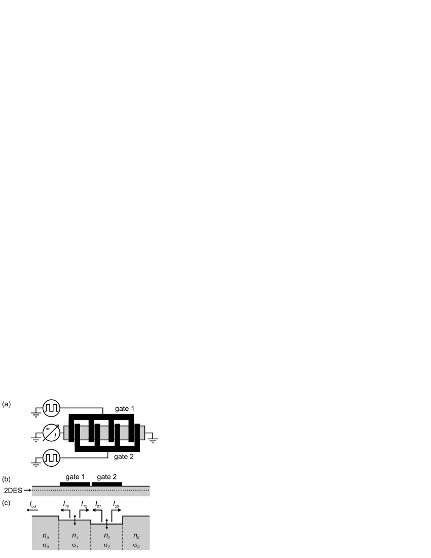
The sample presented here is fabricated from a molecular beam epitaxy grown GaAs/AlxGa1-xAs heterostructure, containing a 2DES below the surface. The electron density and mobility at are and , respectively. Samples from other heterostructures (not presented here) yield similar results. A Hall bar-shaped mesa is fabricated using optical lithography, etching, contact metallization and annealing. On top, two sets of interdigitated gate transducers (IGTs) are defined by electron beam lithography and subsequent metallization. Each set consists of 75 gate stripes, (each wide) interlacing off center by two thirds of the lattice period of . A schematic top view of the sample is shown in Fig. 1(a). Measurements are performed inside a cryostat at a base temperature of . temp The dc source-drain pumping current is measured using a transimpedance-converter, whose output signal is filtered by an eight-pole low-pass Bessel-filter, set to a corner frequency of . The same waveform – with a well-defined phase difference – is applied to the two sets of gates, using two frequency-locked arbitrary waveform generators. The signals applied to gates 1 and 2 can be expressed as and , respectively, where represents one of the normalized amplitude waveforms – sine, rectangle or triangle – the frequency, the time and the amplitude. In order to eliminate parasitic currents, which, i. e., result from thermal voltages or the rectification of capacitive currents inside the non-ideal AuGe-contacts, we measure the output current in the interval and define the pumping current for .
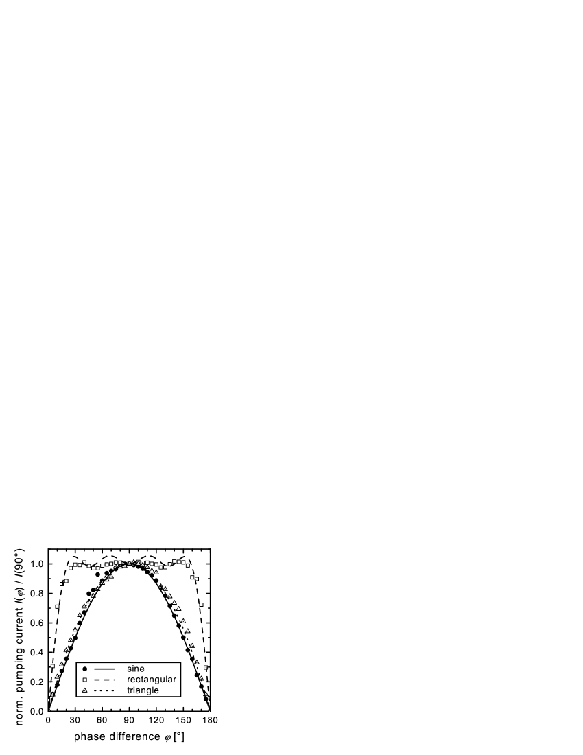
Figure 2 shows experimental, normalized -traces for different waveforms at a frequency of and an amplitude . The symbols represent the experimental results. The fact, that the pumping current as a function of the phase difference, especially for the sine and rectangular signals, closely resembles the waveform of the pumping signal is somewhat surprising and will be analyzed in more detail below. Since the phase can be changed arbitrarily slow, this observation may open possibilities for novel wave sampling devices, even for very high frequencies.
For a deeper understanding whether our experimental results are coincidental for the present device or are a general feature of adiabatically driven ratchets in 2DESs, we develop a simple hydromechanical model of adiabatic electron pumping in the artificial superlattice. It is based on a single unit cell (one period of the superlattice), as shown in Figs. 1(b) and 1(c). As, in the present experiment, we use temporal periods which are much longer than all relevant relaxation times of the electron system, we can use an adiabatic approximation. For a treatment of the high frequency limit, see ref. dittrich2003 . The unit cell is divided in three regions, as can be seen in Fig. 1(c). Due to capacitive coupling between the gate electrodes and the 2DES, we assume a linear relationship between the applied gate voltage and the electron density inside the respective region . If we restrict the discussion to small gate voltages only (, where is the voltage at which the 2DES is fully depleted), we can assume the conductivity to be only depending on , via , neglecting small changes of the mobility . By changing the electrons have to move from (to) neighboring regions 0 and 2 into (out of) region 1. The ratio of electrons moving from (to) area 0 and 2, respectively, is determined by Kirchhoff’s laws. Using this result, one can derive, i. e., the current from region 1 into region 2:
| (1) |
This results in an output current of the unit cell of
| (2) | |||||
By inserting Fourier series expansions of the respective time-dependent electron-densities (as defined by the waveforms applied to the IGTs), one can evaluate the dc pumping current of the device, by integrating the output current over one temporal period of the input waveform. For the sine waveform, the result is plotted in Fig. 2 as a solid line which reproduces the experimental findings very well.
In order to model more complex waveforms, we have to consider that in any real sample, a RC cutoff frequency will be present, which suppresses the higher Fourier components of the modulation signal. To account for this experimentally determined cutoff frequency of , we have weighted the Fourier components by a 3-term-Blackman-Harris distribution. blackman-harris If we assume , we only have to include the first seven Fourier components into our calculation. The results are plotted as dashed and dotted lines into Fig. 2 for the rectangular and triangular waveforms, respectively. They match remarkably close the experimental data, although effects like the gate voltage dependent mobilities are neglected.
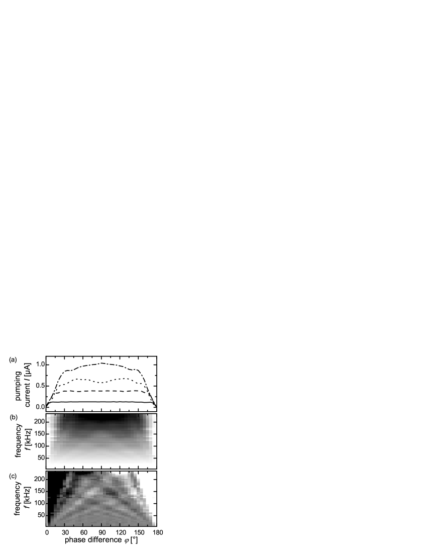
The rectangular waveform pumping current is plotted for different frequencies in Fig. 3(a). It can be clearly seen, that the pumping current increases linearly with the frequency of the gate signal. hoehberger2001 For low frequencies, i.e. , the resulting output waveform nearly perfectly resembles the imposed rectangular waveform. Additional oscillations in the signal can be observed, especially for higher frequencies. They are a direct consequence of the RC constant of the system, which results in higher harmonics being more efficiently attenuated at higher operating frequencies. With increasing the traces become more and more ‘softened’. Ultimately for (not shown here) the current is determined only by the first harmonic, resulting in a nearly sinusoidal output current. To illustrate that the oscillations in the pumping efficiency indeed originate from the effective filtering of the high frequency contributions, a gray scale plot of is presented in 3(b). In order to emphasize the fine-structure, the derivative is numerically calculated and plotted against and in fig. 3(c). Apart from the flanks (dark area on the left and bright area on the right hand side of the figure) the oscillatory features extend diagonally from the lower corners of the plot, corresponding to the harmonic components of the rectangular waveform, as predicted by the model.
This damping of the higher harmonics also explains, why the triangular waveform is not reproduced very well. For the triangular waveform the unattenuated Fourier coefficients scale like , while for the rectangle they scale like , with . So the higher Fourier coefficients of the triangular waveform are per-se much weaker than the respective coefficients for the rectangular waveform, resulting in an characteristics, which is mainly dominated by lower harmonics, in particular the first one.
We have presented a method to sample an arbitrary periodic waveform by using interdigitated gates on top of a 2DES. The high frequency operating limit is intrinsically determined by the RC constant of the system, as this leads to the attenuation of higher harmonics. The results were explained within a simple hydromechanical model of adiabatic electron pumping. The described system may serve as the foundation for future signal sampling devices in solid state electronics. Following our proof-of-principle, better device parameters will lead to a higher cutoff frequency, eventually allowing a very high frequency operation of the device.
References
- (1) D. J. Thouless, Phys. Rev. Lett. 27, 6083 (1983), P. W. Brouwer, Phys. Rev. B 58, R10135 (1998), B. L. Altshuler and L. I. Glazman, Science 283, 1864 (1999), and references therein.
- (2) For a review, see i. e. P. Reimann, Phys. Rep. 361, 57 (2002) and the special issue of Appl. Phys. A 75, (2002).
- (3) R. P. Feynman, R. B. Leighton, and M. Sands, The Feynman Lectures in Physics (Addison-Wesley, Reading, MA, 1966).
- (4) H. Pothier et al., Europhys. Lett. 17, 249 (1992).
- (5) S. V. Lotkhov et al., Appl. Phys. Lett. 78, 946 (2001).
- (6) P. Delsing et al., Phys. Rev. Lett. 63, 1861 (1989).
- (7) L. J. Gerlings et al., Phys. Rev. Lett. 64, 2691 (1990).
- (8) J. M. Martinis, M. Nahum, and H. D. Jensen, Phys. Rev. Lett. 72, 904 (1994).
- (9) M. W. Keller et al., Science 285, 1706 (1999).
- (10) L. P. Kouwenhoven et al., Phys. Rev. Lett. 67, 1626 (1991).
- (11) M. Switkes et al., Science 283, 1905 (1999).
- (12) V. I. Talyanksii et al., Phys. Rev. B 56, 15180 (1997) and M. Rotter et al., Phys. Rev. Lett. 82, 2171 (1999).
- (13) For a review, see i. e., W. G. Ong, Modern MOS Technology: Processes, Devices and Design (McGraw-Hill, Singapore, 1987).
- (14) E. M. Höhberger et al., Appl. Phys. Lett. 78, 2905 (2001).
- (15) For the pumping principle the temperature is of little relevance and similar results have been found up to a temperature of , where gate leakage currents become detrimental to the experiment.
- (16) Normalized in this context implies a peak-to-peak value of 1 for each given waveform.
- (17) T. Dittrich, M. Gutiérrez, and G. Sinuco, Physica A 327, 145 (2003).
- (18) H. Günzler and H. U. Gremlich, IR-Spectroscopy (Wiley-VCH, Weinheim, 2002).