Anti-ferromagnetic ordering in arrays of superconducting -rings
Abstract
We report experiments in which one dimensional (1D) and two dimensional (2D) arrays of YBa2Cu3O7-δ-Nb -rings are cooled through the superconducting transition temperature of the Nb in various magnetic fields. These -rings have degenerate ground states with either clockwise or counter-clockwise spontaneous circulating supercurrents. The final flux state of each ring in the arrays was determined using scanning SQUID microscopy. In the 1D arrays, fabricated as a single junction with facets alternating between alignment parallel to a [100] axis of the YBCO and rotated to that axis, half-fluxon Josephson vortices order strongly into an arrangement with alternating signs of their magnetic flux. We demonstrate that this ordering is driven by phase coupling and model the cooling process with a numerical solution of the Sine-Gordon equation. The 2D ring arrays couple to each other through the magnetic flux generated by the spontaneous supercurrents. Using -rings for the 2D flux coupling experiments eliminates one source of disorder seen in similar experiments using conventional superconducting rings, since -rings have doubly degenerate ground states in the absence of an applied field. Although anti-ferromagnetic ordering occurs, with larger negative bond orders than previously reported for arrays of conventional rings, long-range order is never observed, even in geometries without geometric frustration. This may be due to dynamical effects. Monte-Carlo simulations of the 2D array cooling process are presented and compared with experiment.
I Introduction
In superconducting rings, the requirement of a single-valued, macroscopic quantum mechanical wave-function, combined with the intimate relation between the quantum mechanical phase and the vector potential, results in flux quantization.deaver1961 ; doll1961 Under the appropriate conditions, two of the flux quantized states can become degenerate, characterized by time-reversed, persistent supercurrents circulating in a clockwise and counter-clockwise direction. These macroscopic circulating currents can be thought of as an analog to an electronic spin. In pioneering work, Davidovic et al.davidovic1996 ; davidovic1997 showed that arrays of superconducting rings can be used as models for spin systems, since they interact anti-ferromagnetically upon cooling. However, the Davidovic arrays never showed long-range anti-ferromagnetic ordering. They speculated that one reason for this lack of ordering is that, for there to be two degenerate states, such rings must be cooled in a field equivalent to a half-integer multiple of the superconducting flux quantum per ring. Therefore variations in the lithographically patterned areas of these rings result in different fluxes through different rings in the same field, causing disorder. Superconducting -rings have an intrinsic phase shift of in the absence of an externally applied field or supercurrent. bulaevskii1977 ; geshkenbein1986 ; geshkenbein1987 Such rings have a doubly degenerate ground state in zero applied flux, should not have this source of disorder, and may therefore be a more ideal model for a spin system.
However, use of -rings for a model spin system requires a large number of rings. The first superconducting -rings,wollman1993 ; brawner1994 ; tsuei1994 ; mathai1994 which depended on the momentum dependence of the pairing wavefunction in the high-Tc cuprate perovskite superconductors, were made using technologies which would be difficult to extend to many devices. Recently a technology that allows for photolithographic fabrication of -shift devices and arrays of great complexity, using YBa2Cu3O7-δ-Au-Nb (YBCO-Au-Nb) ramp-edge tunneling junctions has been demonstrated.smilde2002a ; smilde2002b Moreover, it has recently been demonstrated that -rings can also be fabricated using Josephson junctions with ferromagnetic layers in the tunnel barriers. andreev1991 ; ryazanov2002 ; bauer2004 In this paper we report on experiments in which the YBCO ramp-edge technology was used to fabricate large arrays of -rings. A first report on work with similar arrays appeared in Ref. hilgenkamp2003, . The arrays were cooled in various magnetic fields, and the final “spin” states of the arrays were determined with scanning SQUID microscopy. Long range anti-ferromagnetic (AFM) ordering was observed in the 1D arrays. Although stronger anti-ferromagnetic correlations were observed in our 2D -ring arrays than were reported previously for the conventional (-ring) arrays, in neither case did AFM ordering extend beyond a few lattice sites. Although using -rings eliminated one source of disorder, inhomogeneous flux biasing due to the applied fields required for -rings, there are other sources of disorder, including inhomogeneities in the ring critical currents and critical temperatures. We will discuss the influences of these sources on our results, as well as dynamic effects, using Monte-Carlo modelling of the cooling process.
II Experimental methods
Various samples consisting of one- and two-dimensional -ring arrays have been realized using ramp-type YBa2Cu3O7-δ - Au - Nb Josephson contacts. The fabrication of ramp-type YBa2Cu3O7-δ - Au - Nb Josephson has been described previously in detail in Ref.’s smilde2002a, ; smilde2002b, . In short, the samples were prepared by first epitaxially growing a bilayer of [001]-oriented YBa2Cu3O7-δ and SrTiO3 by pulsed-laser deposition on [001]-oriented SrTiO3 single crystal substrates. For the 1D array samples a 150 nm YBa2Cu3O7-δ and a 100 nm SrTiO3 film were used, while for the 2D array samples a 340 nm YBa2Cu3O7-δ and a 67 nm SrTiO3 film were used. In these bilayers the basic layout of the structures, which will be described below in more detail, is defined by photolithography and Ar ion milling. This process results in interfaces with a slope of with respect to the substrate, which provides access to the -planes of the YBa2Cu3O7-δ and allows the exploitation of -wave phase effects. Special care is taken to align all interfaces accurately along one of the YBa2Cu3O7-δ [100] axes. After etching the ramp and cleaning of the sample, a 7 nm YBa2Cu3O7-δ interlayer is deposited, the function and properties of which are described in Ref. smilde2002b, , followed by the in-situ pulsed-laser deposition of a Au barrier-layer of 12 nm for the 1D array samples and 20 nm for the 2D array samples. A 160 nm Nb counter electrode is then formed by dc sputtering and structured by lift-off. Each chip contained several reference-junctions. At T = 4.2 K, these showed a typical critical current per micrometer junction-width mA/m for the 1D array samples and mA/m for the 2D array samples. From these, a value for the Josephson penetration depth m (T = 4.2 K) for all samples is deduced, which is the characteristic length scale over which Josephson vortices (fluxons) extend.
The sample magnetic fields were imaged with a high resolution scanning SQUID microscope.rogers1983 ; vu1993 ; black1993 ; kirtley1995 The SQUID microscope images shown here were made at a temperature of T 5K, with the sample cooled and imaged in the same fields. The size of the pickup loop used will be indicated for each image. The samples were warmed through the superconducting critical temperature of the Nb and cooled at controlled rates either using a non-inductive heater, or by passing warm 4He gas past the sample.
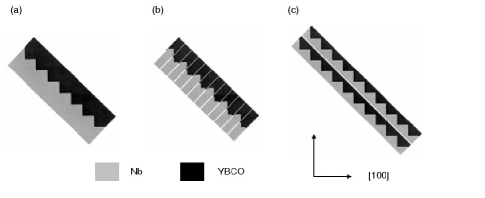
A first configuration for which the generation and coupling of half-integer flux quanta was investigated is the zigzag array,smilde2002a several instances of which are shown schematically in Figure 1. In these structures, the -wave order parameter of the YBa2Cu3O7-δ induces a difference of in the Josephson phase-shift across the YBa2Cu3O7-δ-Au-Nb barrier for neighboring facets. For facet lengths in the wide limit, i.e., , the lowest-energy ground state of the system is expected to be characterized by a spontaneous generation of a half-integer flux-quantum at each corner. This half-fluxon provides a further -phase change between neighboring facets, either adding or subtracting to the -wave induced -phase shift, depending on the half-flux quantum polarity. In both cases this leads to a lowering of the Josephson coupling energy across the barrier, as this energy is proportional to (1 - cos ). We studied three types of facetted junctions. The first (Fig. 1a) was an isolated, continuous junction with many adjacent facets. The second (Fig. 1b) was lithographically patterned to electrically isolate each half-fluxon from its neighbor. The final type (Fig. 1c) had two continuous facetted junctions close together, but electrically isolated from one another, to test for field coupling between 1D arrays of half-fluxons.
| Square | Triangular | Honeycomb | Kagomé | |
| height YBCO (nm) | 340 | 340 | 340 | 340 |
| height STO (nm) | 67 | 67 | 67 | 67 |
| height Nb (nm) | 160 | 160 | 160 | 160 |
| width JJ 1 (m)1 | 2.75 | 2.70 | 2.70 | 2.70 |
| width JJ 2 (m)1 | 2.75 | 3.75 | 3.75 | 3.75 |
| hole (m) | 2.50 | 3.10 | 3.10 | 3.10 |
| self-inductance (pH)2 | 3.93 | 3.90 | 3.90 | 3.90 |
| self-inductance (pH)3 | 4.57 | - | - | - |
| nearest neighbor | 11.5 | 11.5 | 11.5 | 11.5 |
| distance (m) | ||||
| nearest neighbor | 0.025 | - | - | - |
| mutual (pH)3 | ||||
| 1 designed value | ||||
| 2 estimate with standard formulas | ||||
| 3 estimate using FastHenry, =160nm and =40nm | ||||
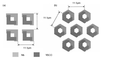
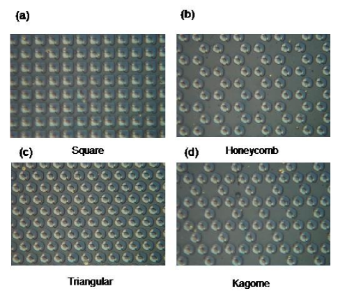
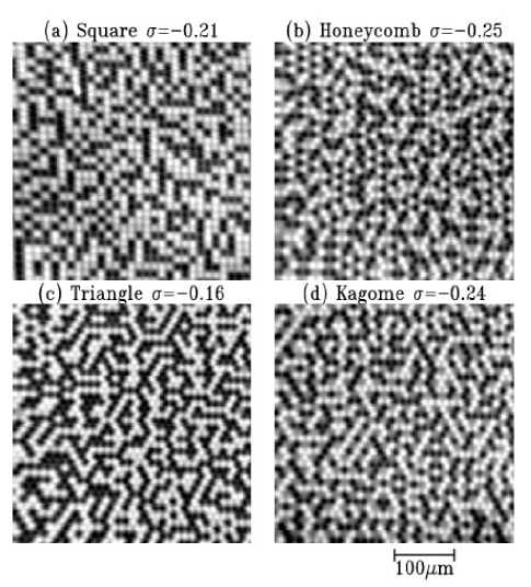
The 2-dimensional -ring arrays were made up of individual rings patterned as indicated schematically in Figure 2. There were two types of rings, square (Fig. 2a) and hexagonal (Fig. 2b). The rings were patterned into arrays with 4 different geometries, as shown in the scanning electron microscopy images of Figure 3. In all cases the nearest-neighbor distances in these arrays was 11.5m center to center. The details of the ring geometries, critical currents, self-inductances, and mutual-inductances are given in Table 1.
III Results
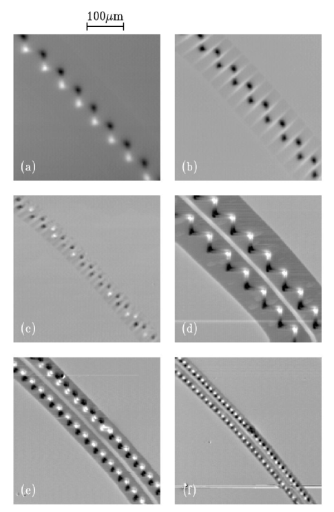
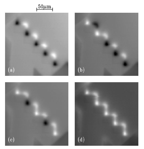
Figure 4 shows representative scanning SQUID microscope images of 6 zigzag facet junctions. All of these images were of samples on the same substrate, and imaged in the same cooldown in nominal zero field ( T) at T = 4.2K. In all three types of facetted junctions, half-fluxon Josephson vortices were spontaneously generated at the points where the facets met, as expected. When the connected 1D arrays (Fig. 1a) were cooled in zero field through the niobium superconducting transition temperature, the signs of the half-fluxons strongly tended towards perfect anti-ferromagnetic ordering, in which the persistent supercurrents alternated between clock-wise and counter clock-wise flow (Fig. 4a,d,e,f). There are two possible mechanisms for this ordering. In the first, ordering is driven by the minimization of the total junction Josephson coupling energy during the cooling process. We refer to this as “phase” coupling, because the Josephson currents and energies are determined by the difference in superconducting phase across the junction . In the second, the anti-ferromagnetic ordering is driven by a minimization of the total magnetic field energy in the junction and its environment. We refer to this as “field” coupling. In order to determine the relative strengths of these mechanisms, facetted junctions were fabricated with each half-fluxon electrically isolated from its neighbor (Fig. 1b). This should eliminate the phase coupling mechanism. Indeed, when this is done the anti-ferromagnetic ordering in these 1D arrays is much weaker. Two examples are shown in Fig. 4b,c. In Fig. 4b the half-fluxons all have the same orientation. We believe that this is because they align with a small residual field. Fig. 4c shows a more random alignment of the isolated half-fluxons.
In order to test for magnetic field coupling between the 1D half-fluxon chains, double facetted junctions (Fig. 1c) were also fabricated and tested. It appeared that also in this case the phase coupling was stronger than the field coupling: Fig. 4d shows a section of a 40m facet double junction that shows in-phase alignment between the two anti-ferromagnetically ordered 1D chains. Because this arrangement places the positive half-fluxons in the lower left chain closest to the negative half-fluxons in the upper right chain, this is the lowest energy arrangement. However, in sections of the 1D chains which show defects, as in the center of the upper right chains in Fig. 4e and Fig. 4f, the interchain alignment goes from in-phase to out-of-phase when the interchain ordering has a defect, but one chain does not develop a second defect to align the interchain spins. Therefore it appears that the energy cost to create a defect is larger than the energy gain from making neighboring chains in-phase.
When the facetted junctions are cooled in an externally applied magnetic field, one spin direction becomes energetically favored over the other, but there is a competition between this energy and the anti-ferromagnetic coupling energy during the cooling process. An example is shown in Figure 5. More detailed results and modelling of this facetted junction will be described in the next section.
In the electrically disconnected 2D lattices of Fig. 3, the square and honeycomb arrays are geometrically unfrustrated, as their magnetic moments can be arranged so that all nearest neighbors have opposite spins. In contrast, the triangle and kagomé lattices are geometrically frustrated, since it is impossible for all of the rings to have all nearest neighbors anti-ferromagnetically aligned. Fig. 6 shows examples of scanning SQUID microscope images of the arrays of Fig. 3 after cooling in nominally zero field. Although regions of perfect anti-ferromagnetic ordering are seen in the unfrustrated arrays (Fig. 6a,b), anti-ferromagnetic ordering beyond a few lattice distances was never observed. Nevertheless, antiferromagnetic correlations were seen in all the 2D -ring arrays. A measure of the short range antiferromagnetic correlations is the bond order
| (1) |
where is the fraction of the nearest neighbor pairs with opposite supercurrent circulation, and () is the fraction of rings which have up (down) moments. Perfect antiferromagnetic correlation would correspond to = -1. The minimum possible bond order at zero applied field for the frustrated triangular and kagomé lattices is = -1/3.davidovic1997 The images in Fig. 6 are labelled with values for the bond orders.
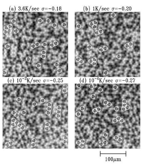
It is to be expected that the anti-ferromagnetic ordering of the 2D arrays should improve if they are cooled more slowly through the Nb superconducting transition. Figure 7 shows SQUID microscope images of the same region of the honeycomb 2D lattice of Fig. 3, after cooling at various rates. The individual panels are labelled with the cooling rates and final state bond orders. The anti-ferromagnetic ordering increases with slower cooling rates. One question that can be asked is: Do particular regions of the 2D array order more strongly than others? The white circles in Fig. 7 outline the 6-member rings in the honeycomb arrays in which all neighbors are anti-ferromagnetically aligned. This provides a convenient way of visualizing regions of local order. It appears that there are no correlations between the positions of the ordered 6-member rings from cooldown to cooldown, and we conclude that the ordered regions are randomly distributed in space.
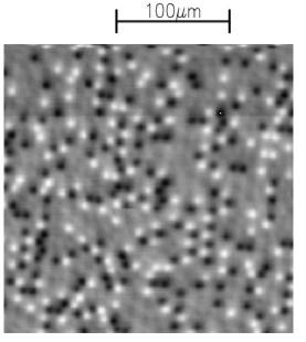
In the -ring experiments of Davidovic et al. davidovic1996 ; davidovic1997 repeated cooling resulted in a particular ring often being in the same final state (spin-up or spin-down). This is presumably the result of the rings having slightly different effective areas, and therefore cooling in slightly different effective fields, since -rings must be cooled in finite fields for there to be degenerate states. The individual rings in our 2D -ring arrays appear to have random final states. Figure 8 shows a difference image between Fig. 7b and Fig. 7c, which were taken after successive cooldowns. In this image, the rings which did not switch sign from one cooldown to the next are not visible, the rings which switched from down to up appear black, while the rings which switched from up to down appear white. Of the roughly 663 rings in this field of view, 152 switched from down to up, and 162 switched from up to down. This is consistent with random switching during cooldown.
IV Modelling
For the current purposes we treat the facetted ramp edge junction as a linear junction with alternating regions of - and - intrinsic phase shifts extending in the -direction, with the junction normal in the direction, and the junction width in the direction small compared with the Josephson penetration depth , where is the spacing between the superconducting faces making up the junction, and is the Josephson critical current per area of the junction. The quantum mechanical phase drop across the junction is the solution of the Sine-Gordon equation:
| (2) |
Analytical solutions to this equation are available,xu1995 ; susanto2003 ; kogan2000 but here we solve Eq. 2 numerically.scalgbj ; goldobin2002 ; goldobin2003 ; zenchuk2004 ; goldobin2004c Defining a dimensionless coupling parameter
| (3) |
the differential equation Eq. 2 turns into a difference equation on a grid of size :
| (4) |
Taking the net current across the junction equal to zero, using a reduced externally applied magnetic field , and using the relation between the gradient of the phase and the field in the junction:
| (5) |
we find boundary conditions that are described as difference equations, where is the total number of junctions:
| (6) |
These coupled difference equations are solved using a relaxation method to find the solution , iterating to convergence. As the junction cools through the superconducting transition temperature Tc, the supercurrent density increases from zero, so that decreases from infinity. To model the cooling process, we first solve Eq. 4 for much larger than the facet length , then decrease by a small amount, take the previous solution as the starting point for the next solution, and repeat until . An example is shown in Fig. 9. Here the externally applied flux was set at , the total junction length =400m, =1m, with 10 facets each of length =40m, an initial , which was decreased to 4m in 24 equal steps. The field threading the junction is given by . The final solution strongly favors anti-ferromagnetic arrangement of the half-fluxon “spins”.
We can understand why the facetted junctions cool into perfect anti-ferromagnetic order, while the isolated linear arrays of -rings do not, by considering the energetics of the cooling process. Written as a difference equation, the free energy for a particular state of the facetted junction becomes:
| (7) |
Numerical solution of the Sine-Gordon equation as described above for the facetted junction of Fig. 5 shows that the free energy/facet, when the junction is in perfect anti-ferromagnetic ordering, is -5105K/(m). The energy cost to form a defect, by flipping one spin, is 7.2105e. This implies that when the free energy/facet is comparable to kBT, the energy cost to form a defect is 7.2105K : it is energetically favorable to form perfect anti-ferromagnetic ordering in linear facetted junctions cooled in zero field.
Figure 10 compares the results from repeated cooling of the 10-facet zigzag junction under various magnetic fields with modelling using the numerical solution of the sine-Gordon equation outlined above. Note that there are some disorder effects in the cooling process, as evidenced by the slight differences between the two experimental runs. The qualitative features of the data are reproduced by the modelling, although the experimental results are not as symmetric with respect to inversion in position, or with respect to field reversal, as predicted. One possible source of the observed asymmetry might be field gradients. However, putting a linear field gradient into the model did not improve the fit with experiment. Another source of asymmetry might come from the asymmetry of the junction and lead geometry.
The cooling process for isolated -rings is different than for electrically connected -rings. For simplicity we model our isolated -rings considering a single inductance and Josephson junction critical current . The details of the formulas will be different for a two-junction ring,smildeprb but we do not expect the physics to be qualitatively different. The free energy U of such a -ring can be written as
| (8) |
where is the magnetic flux included in the ring, and is the flux externally applied to the ring. At temperatures important in the cooling process, close to the Nb superconducting transition temperature Tc, field screening effects can be neglected, since the magnetic penetration lengths are larger than the size of the sample. Under these conditions, we estimate the ring self-inductances (for 2.7m junction width rings spaced by 11.5m) to be 3.9pH, and the mutual inductance M between nearest neighbor rings to be 0.025pH. For a single junction -ring spontaneous supercurrents flow when is just greater than 1. The ring ordering process will occur in the regime . In this limit, and in the limit , where is the magnetic flux applied per ring, the potential barrier to flipping the sign of the ring supercurrents in the ring can be approximated by
| (9) |
with , where is the spin of the ring, and
| (10) |
where is the externally applied flux and is the mutual inductance between the and rings. In the same limits, the value of the spontaneous flux generated by the ring is given by
| (11) |
We take the junction critical current Ic(0)=0.55mA for these rings, and the self-inductance of the rings is assumed to be temperature independent. A measure of the spin-spin coupling energy is the difference between the energy barrier for all nearest neighbor spins up, minus that energy barrier if one of the neighbor spins is down.
Fig. 11 plots the calculated barrier to thermally activated flipping , nearest neighbor coupling energy , and the thermal energy as a function of temperature for the honeycomb ring array of Fig. 6. Both Eb and Ec increase as the temperature is lowered until the flipping freezes out at a temperature such that , where .cosmoprl For the rings of Fig. 6, we estimate this occurs at = 310-2, with and . At this temperature . Therefore antiferromagnetic coupling is energetically favored in isolated -rings, but not nearly as strongly as in facetted junctions.
As the temperature is lowered through , the junction critical currents increase until two distinct circulating states become allowed for . Thermally activated switching between these states has a transition rate
| (12) |
where is the junction hysteresis parameter, and is the junction characteristic time.tesche1981 We take the junction capacitance , , , and =1 for the 2D arrays presented in this paper. We have taken the limits where the d.c. shielding currents are much smaller than the critical currents, the spin-flip transition times are much shorter than the time between spin-flips, and . We can isolate the temperature dependence of the prefactor of Eq. 12 by writing . It is of interest to note that the power dissipated per ring near the “freezout” temperature is of order .
To model the cooling process in our 2D ring arrays we use a Metropolis Monte Carlometropolis simulation: A 30x30 element array is set up with the same geometry as the experimental arrays. Boundary effects are minimized by using periodic boundary conditions: rings at one edge of the array are treated as if their nearest neighbors are the corresponding rings at the opposite edge. The results of our simulations do not depend sensitively on whether periodic or non-periodic boundary conditions are used. For each iteration cycle, the probability of a spin flip ,
| (13) |
is calculated for each ring. A random number between and is generated. If this number is less than , the spin of the ring is flipped. The process is repeated throughout the array, and the temperature is gradually reduced until no more spin flips occur. Figure 12 shows results from a Monte-Carlo simulation of the honeycomb lattice of Fig. 3, using the ring parameters of Table I, plotting the bond order as a function of the reduced temperature , for various values of , the change in per iteration cycle. Note that in this case the maximum temperature for which spontaneous magnetization is observed is . As the temperature is reduced the spin flipping probabilities decrease, and anti-ferromagnetic ordering gradually occurs. Furthermore note that the freezing temperature is well below the temperature at which . The effective cooling rate of the simulation is given by K-sec-1. Therefore the slowest cooling rate simulated is about K/sec, much faster than the experimental cooling rates. Although it would in principle be possible to use sufficient computer time to match the modelled cooling rates to experiment, the modelling indicates stronger anti-ferromagnetic ordering than is observed, even at these very fast cooling rates.
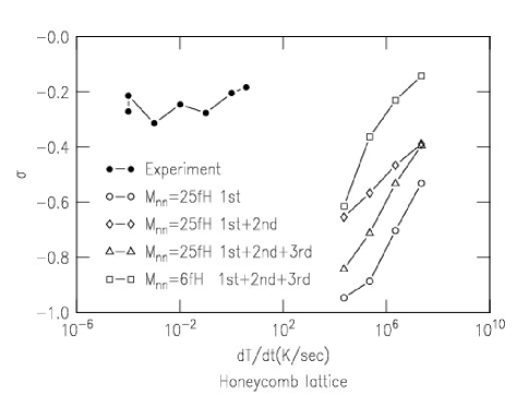
Figure 13 shows experimental results for the final bond order for the honeycomb array of Fig. 6, for various cooling rates. Experimentally the effect of cooling rate on final bond-order is weak. Also shown in this Figure are the results of our Monte-Carlo simulations for the honeycomb array. The points labelled use all of the parameters in the simulation as calculated following Table I. The points labelled used a reduced value of the ring-ring mutual inductance. Also shown are curves comparing the predictions if only the nearest neighbor spin-spin interactions are included, with results if 2nd and 3rd nearest neighbors are also included. The mutual inductance between a ring and its further neighbors (e.g. 2nd nearest and 3rd nearest) is taken to be scaled by the cube of the ratio of the relevant center-to-center distances. Qualitatively, the inclusion of next nearest neighbors reduces the tendency towards anti-ferromagnetic ordering. However, it appears that the inclusion of 3rd nearest neighbors does not change the results much further. Similarly, reducing the strength of the spin-spin coupling by a factor of 4 also reduces the tendency to order. However, in all cases it appears that if the simulation were to be extended to sufficiently slow cooling rates to match experiment, long-range ordering would result.
This failure of our arrays to order implies that there is a source of disorder that we haven’t taken into account. There are three additional sources of disorder that we have considered. The first is a distribution in Nb critical temperatures, and the second is a distribution in junction critical currents. In each case, our simulations indicate that an unrealistically large distribution width is required to significantly effect the predicted final value vs. cooling rate curves. In all the cases we have explored numerically: reducing , reducing , increasing the width of the Tc distribution, or increasing the width of the distribution, the vs. cooling rate curves can be shifted vertically in Fig. 13, but the slope of these plots does not change qualitatively. A final factor that might inhibit ordering of our arrays is if the cooling rate is not uniform. However, inspection of Fig. 12 indicates that fast jumps in temperature of order 0.01 would be required to significantly affect the final bond-orders. It seems unlikely that our temperature sweeps are that non-uniform. It is therefore difficult to see how the experimental data can be fit using the present simulations, and some factor that we haven’t considered correctly is causing the failure of our arrays to achieve long range order.
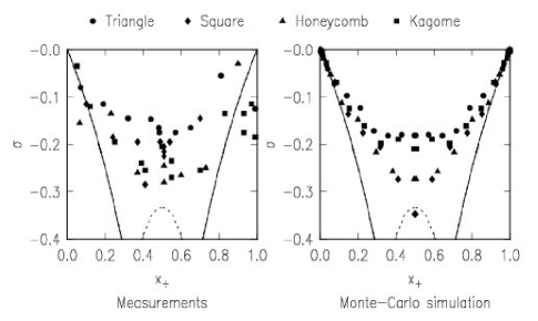
Nevertheless, the experimentally determined values for the bond-order can be modelled fairly well, if one uses the cooling rate as a fitting parameter. The left-hand panel of Fig. 14a summarizes cooling experiments for all of the 2D arrays of Fig. 6. These data were taken after cooling the arrays at rates between 1mK/sec and 10mK/sec. Although long-range anti-ferromagnetic order was not observed in these arrays, they did show strong anti-ferromagnetic correlations, as evidenced by the large negative bond orders. Note that there are no qualitative differences between the geometrically frustrated and non-frustrated lattices in their tendency to anti-ferromagnetically order. For comparison, the -rings of Ref. davidovic1996, ; davidovic1997, never showed bond-orders more negative than , whereas our -ring arrays attained bond orders as negative as . The right hand panel shows the results of Monte-Carlo simulations for these arrays, using the ring parameters in Table I, except for instead of , and with a cooling rate . In both panels the ideal curve for an unfrustrated lattice (solid line) and a frustrated lattice (dashed line) are also indicated. The experimental results can be qualitatively modelled assuming a spin-spin coupling constant about 4 times smaller than calculated, and a cooling rate times faster than the experiment.
V Conclusions
We have shown that it is possible to use large arrays of photolithographically patterned -rings as a model spin system. Half-fluxon Josephson vortices in electrically connected 1D arrays, in the form of zigzag facetted junctions, order strongly anti-ferromagnetically through the superconducting order parameter phase. Electrically isolated 1D and 2D arrays order much less strongly. The 2D -ring arrays show stronger anti-ferromagnetic correlations than reported previously for -ring arrays, but not long-range order beyond a few lattice constants. We can understand the anti-ferromagnetic phase coupling of the 1D zigzag junctions by solving the Sine-Gordon equations. Although some features of the ordering in the 2D arrays can be understood using Monte-Carlo simulations, unrealistic parameters must be used, and we do not understand why these arrays do not show long range order.
VI Acknowledgements
We would like to thank D.H.A. Blank, R.H. Koch, K.A. Moler, G. Rijnders, and H. Rogalla for useful discussions. We also acknowledge the Dutch Foundations FOM and NWO for supporting this research.
References
- (1) B.S. Deaver and W.M. Fairbank, Phys. Rev. Lett. 7, 43 (1961).
- (2) R. Doll and M. Näbauer, Phys. Rev. Lett. 7, 51 (1961).
- (3) D. Davidovic et al., Phys. Rev. Lett. 76, 815 (1996).
- (4) D. Davidovic et al., Phys. Rev. B 55, 6518 (1997).
- (5) L.N. Bulaevskii, V.V. Kuzii, and A.A. Sobyanin, JETP Lett. 25, 290 (1977).
- (6) V.B. Geshkenbein and A.I. Larkin, JETP Lett. 43, 395 (1986).
- (7) V.B. Geshkenbein, A.I. Larkin, and A. Barone, Phys. Rev. B 36, 235 (1987).
- (8) D.A. Wollman, D.J. Van Harlingen, W.C. Lee, D.M. Ginsberg, and A.J. Leggett, Phys. Rev. Lett. 71, 2134 (1993).
- (9) D.A. Brawner and H.R. Ott, Phys. Rev. B 50, R6530 (1994).
- (10) C.C .Tsuei et al., Phys. Rev. Lett. 73, 593 (1994).
- (11) A. Mathai, Y. Gim, R.C. Black, A. Amar, and F.C. Wellstood, Phys. Rev. Lett. 74, 4523 (1994).
- (12) H.J.H. Smilde et al., Phys. Rev. Lett. 88, 057004 (2002).
- (13) H.J.H. Smilde, H. Hilgenkamp, G. Rijnders, H. Rogalla, and D.H.A. Blank, Appl. Phys. Lett. 80, 4579 (2002).
- (14) A.V. Andreev, A.I. Buzdin, and R.M. Osgood, III, Phys. Rev. B 43, 10124 (1991).
- (15) V.V. Ryazanov, V.A. Oboznov, A.V. Veretennikov, and A. Yu. Rusanov, Phys. Rev. B 65, 020501(R) (2001).
- (16) A. Bauer et al., Phys. Rev. Lett. 92, 217001 (2004).
- (17) H. Hilgenkamp et al., Nature 422, 50 (2003).
- (18) F.P. Rogers, Master’s Thesis, MIT, Boston, (1983).
- (19) L.N. Vu and D.J. van Harlingen, IEEE Trans. Appl. Supercond. 3, 1918 (1993).
- (20) R.C. Black et al., Appl. Phys. Lett. 62, 2128 (1993).
- (21) J.R. Kirtley et al., Appl. Phys. Lett. 66, 1138 (1995).
- (22) D. Xu, S.K. Yip, and J.A. Sauls, Phys. Rev. B 51, 16233 (1995).
- (23) H. Susanto, S.A. van Gils, T.P.P. Visser, Ariando, H.J.H. Smilde, H. Hilgenkamp, Phys. Rev. B 68, 104501 (2003).
- (24) V.G. Kogan, J.R. Clem, and J.R. Kirtley, Phys. Rev. B 61, 9122 (2000).
- (25) J.R. Kirtley, K.A. Moler, and D.J. Scalapino, Phys. Rev. B 56, 886 (1997).
- (26) E. Goldobin, D. Koelle, and R. Kleiner, Phys. Rev. B 66, 100508(R) (2002).
- (27) E. Goldobin, D. Koelle, and R. Kleiner, Phys. Rev. B 67, 224515 (2003).
- (28) A. Zenchuk and E. Goldobin, Phys. Rev. B 69, 024515 (2004).
- (29) E. Goldobin, N. Stefanakis, D. Koelle, and R. Kleiner, Phys. Rev. B 70, 094520 (2004).
- (30) H.J.H. Smilde, Ariando, D.H.A. Blank, H. Hilgenkamp, and H. Rogalla, Phys. Rev. B 70, 024519 (2004).
- (31) J.R. Kirtley, C.C. Tsuei, and F. Tafuri, Phys. Rev. Lett. 90, 257001 (2003).
- (32) C.D. Tesche, J. Low. Temp. Phys. 44, 119 (1981).
- (33) N. Metropolis, A. W. Rosenbluth, M. N. Rosenbluth, A. H. Teller, and E. Teller, J. Chem. Phys. 21, 108 (1953).