Transport properties of diluted magnetic semiconductors: Dynamical mean field theory and Boltzmann theory
Abstract
The transport properties of diluted magnetic semiconductors (DMS) are calculated using dynamical mean field theory (DMFT) and Boltzmann transport theory. Within DMFT we study the density of states and the dc-resistivity, which are strongly parameter dependent such as temperature, doping, density of the carriers, and the strength of the carrier-local impurity spin exchange coupling. Characteristic qualitative features are found distinguishing weak, intermediate, and strong carrier-spin coupling and allowing quantitative determination of important parameters defining the underlying ferromagnetic mechanism. We find that spin-disorder scattering, formation of bound state, and the population of the minority spin band are all operational in DMFT in different parameter range. We also develop a complementary Boltzmann transport theory for scattering by screened ionized impurities. The difference in the screening properties between paramagnetic () and ferromagnetic () states gives rise to the temperature dependence (increase or decrease) of resistivity, depending on the carrier density, as the system goes from the paramagnetic phase to the ferromagnetic phase. The metallic behavior below for optimally doped DMS samples can be explained in the Boltzmann theory by temperature dependent screening and thermal change of carrier spin polarization.
PACS numbers: 75.50.Pp, 75.10.-b, 75.30.Hx, 75.20.Hr
I introduction
Diluted magnetic semiconductors (DMS) Ohno98 ; Ohno96 ; Matsukura98 ; Reed01 with transition temperatures as high as 150K (GaMnAs at Mn Ohno98 ; Ohno96 ; Matsukura98 ) or even above room temperature (GaMnN, GaMnPReed01 ) are attracting much attention lately in part because of possible ‘spintronic’ applications dassarma01 . The prototypical DMS material is Ga1-xMnxAs with the Mn ions substitutionally replacing Ga at the cation sites. It is widely believed that the ferromagnetism in this material is carrier induced with holes donated by Mn ions mediating a ferromagnetic interaction between the randomly localized Mn spins dassarma03 . The coupling of carrier spins (holes in GaMnAs) and localized moments (Mn impurities) gives rise to the unique magnetic and transport (as well as optical) properties in DMS.
DMS transport properties are influenced by the exchange interaction between the carriers and the localized moments as spin fluctuation scattering contributes to the resistivity. The experimentally measured dc-resistivity in DMS materials Matsukura98 ; oiwa ; hirakawa shows interesting behavior strongly depending on the concentration of the magnetic impurity and temperature. In In1-xMnxAs hirakawa and Ga1-xMnxAs Matsukura98 ; oiwa with low Mn concentration () only an insulating behavior has been observed in transport measurements. However, near optimal doping , where the highest value of is reported, the non-monotonic behavior (insulator-metal-insulator) of the resistivity as a function of temperature is observed. A resistivity peak appears near the critical temperature (), and the resistivity shows metallic behavior () below and insulating behavior () at higher temperatures. The peak has been understood as the critical scattering effects at of spin fluctuations deGennes .
In this paper we present theoretical calculations for DMS transport properties and study the role of the carrier-spin coupling which are crucial for ferromagnetic properties. Transport measurements have proven useful in understanding the physics of the colossal magnetoresistance (CMR) manganites where carrier-spin coupling is also crucial CMRReview . In our calculation we use a recently developed non-perturbative method, the “dynamical mean-field theory” (DMFT),Kotliar for calculating the DMS transport properties. A non-perturbative method is needed in DMS materials because the crucial physics involves bound-state formation and other aspects of intermediate carrier-spin couplings not accessible to perturbative methods. (We note that the most interesting phenomena in DMS involve intermediate couplings and intermediate temperatures. This regime is very difficult to treat by standard analytical or numerical methods.) The DMFT has been recently applied to the DMS system to calculate the magnetic transition temperature and the optical conductivity Chattopadhyay01a ; hwang . DMFT is essentially a lattice quantum version of the Weiss mean field theory where the appropriate density of states (including impurity band formation) along with temporal fluctuations are incorporated within an effective local field theory. An important ingredient of DMFT Chattopadhyay01a is that it reduces to the standard RKKY physics in the weak-coupling regime and the double exchange physics in the strong coupling regime.
Our DMFT results show interesting dependence of resistivity on carrier-spin coupling (), carrier density (), doping of the magnetic material (), and temperature () revealing key features of the underlying physics. We find that our results show many similarities to colossal magnetoresistance (CMR) manganites CMRReview , especially, for a large carrier-spin coupling and near half filling of the impurity band (i.e. in the double exchange regime) since the spin-disorder scattering dominates in this parameter range. However, the DMS dc-resistivity exhibits novel features not found in the CMR in the weak coupling RKKY limit (, where is the band width of the carrier). These novel features arise mainly from the bound state formation of the carrier-local spins and carrier occupation of the minority spin band. The formation of the bound state gives rise to an insulating behavior even if the carrier localization effects are not taken into account. Experimental observation of our predictions should lead to crucial information about bound state formation and impurity band physics in this problem. Even though we focus on III-V compound based DMS such as Ga1-xMnxAs, the results presented in this paper are general for all DMS materials.
An important limitation of DMFT is that it is a non-perturbative local theory that cannot really incorporate spatial fluctuations, and therefore resistive charged impurity scattering with its strong momentum dependence is essentially impossible to handle in DMFT. We therefore consider the Boltzmann transport theory to calculate the resistivity of the DMS systems brey ; brey2 . The Boltzmann theory is used to calculate the charged impurity disorder limited DMS resistivity (whereas the DMFT is used for obtaining the spin disorder limited DMS resistivity). Charged impurity disorder arises here both from the ionized Mn acceptor in GaMnAs as well as other charged defects/impurities invariably present in a semiconductor. Using relaxation time approximation we assume that the Boltzmann resistivity is due to ionized impurities. The carriers (holes) are scattered by the screened Coulomb potential, which we calculate using the linearized Thomas-Fermi (TF) approximation and the random phase approximation (RPA). We find that the dominant temperature dependence of the resistivity comes from the change in the screening length in the high density metallic samples. In the metallic GaMnAs DMS samples the change in the measured resistivity, when the temperature goes from to zero, is about 20% in good agreement with our calculation. In the ferromagnetic state (), as the temperature decreases from , we find strong temperature dependence of the resistivity arising from the low temperature screening function and the thermal change of the carrier densities in each spin-split subband. When all the carriers are polarized (this happens in the low density limit) the screening function is almost independent of temperature and the resistivity is also temperature independent. Inclusion of both spin disorder and ionized impurity disorder in DMS transport is the important ingredient of our theory.
This paper is organized as follows. In Sec. II, we describe our model and our theoretical approach based on the dynamical mean-field theory (DMFT). In Sec. III, we study, in detail, the density of states and describe the formation of the spin polarized impurity band. In Sec. IV, we provide the results of calculated DMS resistivity within DMFT. In Sec. V we calculate the transport resistivity within the Boltzmann transport theory for ionized impurities. In Sec. VI, we summarize our qualitative findings and providing a critical discussion of the applicability of our results to DMS systems. A brief conclusion is given in Sec. VII.
II Model and formalism
Our basic model of DMS systems is that of magnetic dopants (“impurities”) interacting through a local exchange coupling with carriers in the host semiconductor material. The generally accepted Hamiltonian of the system is given by
| (1) |
where describes carrier propagation in the host semiconductor band. For simplicity we consider a host material with a single non-degenerate band. We therefore write
| (2) |
where is the spin index and is a random potential arising from non-magnetic defects in the material (e.g., As antisite defects, unintentional background charged impurities, etc.). The second (magnetic) term in Eq. (1), , describes coupling of the carriers to an array of impurity (e.g. Mn) spins at positions ,
| (3) |
where is the local exchange coupling between the spin of the magnetic impurity and the the spins of the semiconductor carriers, is the (Coulombic) potential arising from the magnetic dopant, are the positions of the magnetic dopants, and is the Pauli matrix. Here we absorb the magnitude of the impurity spin into the coupling (which we take to be positive), and represent the spin direction by the unit vector . The third term in Eq. (1), , is the direct MnMn short-range antiferromagnetic exchange interaction
| (4) |
where is a direct antiferromagnetic exchange coupling between impurity spins.
In this section we approximate our model by neglecting the nonmagnetic random potential, , and the direct antiferromagnetic exchange interaction, . Lattice defects may be playing an important role in determining magnetic and transport properties of the samples, but we assume here that these defects enter our theory only in determining the basic parameters of the model, namely, the density of magnetically active dopants , the hole density , and perhaps the local effective exchange coupling between the holes and the magnetic impurities, and do not include any defects into our model explicitly. We include charged impurity scattering through the Boltzmann equation in section IV of this paper. We believe that the effects of the antiferromagnetic coupling between magnetic impurities are either negligibly small or incorporated into the effective parameters of the model. Actually, in the parameter range of interest to us (), where DMS ferromagnetism typically occurs, the magnetic impurities are separated from each other by non-magnetic atoms, and this short-range antiferromagnetic interaction, which rapidly decays with the distance, should be negligible. These approximations are nonessential and are done in the spirit of identifying the minimal DMS magnetic model of interest. Both of these effects, which may be of quantitative importance in some situations, can be included in the theory by adjusting the parameters of the model or perhaps at the cost of introducing more unknown parameters characterizing these interactions. Recently several theories for DMS ferromagnetism explicitly including spatial disorder effects and antiferromagnetic coupling have been developed priour .
In our DMFT DMS model there are two sources of coupling between the carrier and the impurity magnetic moment: a spin-spin coupling () and a potential scattering (). The crucial physical issues are revealed by the consideration of a ferromagnetic state in which all impurity spins are aligned, say, in the direction. Then the carriers with spin parallel to feel a potential on each magnetic impurity site and anti-parallel carriers feel a potential . These potentials self-consistently rearrange the electronic structure. The spin-dependent part of this rearrangement provides the energy gain which stabilizes the ferromagnetic state. The key physics issue is, evidently, whether the potential is weak (so its effect on carriers near the lower band edge is simply a scattering phase shift) or strong (so only majority spin or perhaps both species of carriers are confined into spin-polarized impurity bands). Recent density functional supercell calculations Sanvito01 suggest that in GaMnAs is close to the critical value for bound state formation for the majority spin systems. Unfortunately, the precise effective values of and are typically unknown in a DMS system, and may have to be extracted experimentally.
We assume that magnetic impurities under consideration enter substitutionally at the cation sites (e. g. Mn impurities at Ga sites) and the III1-xMnxV system as a lattice of sites, which are randomly nonmagnetic (with probability ) or magnetic (with probability ), where now indicates the relative concentration (i.e. per Ga site) of active Mn local moments in IIIMnV. If more complete information about Mn locations on the GaAs lattice becomes available it will be straightforward to incorporate that in the DMFT formalism.
We now introduce the DMFT for the Hamiltonian given by Eq. (1). Within the general scheme of the DMFT, the local (momentum independent) self energy of the system, , can be obtained from the time dependent mean field function. Then the single particle Green function is approximated by
| (5) |
where is the chemical potential. With the local self energy all of the relevant physics may be determined from the local (momentum-integrated) Green function defined by
| (6) | |||||
where is the density of states (DOS) for the noninteracting system. The information of the lattice geometry is included through the noninteracting DOS.
In our model is a matrix in spin index and depends on whether one is considering a magnetic ( or non-magnetic ( site. Since is a local function, it is the solution of a local problem specified by a mean-field function , which is related to the partition function with action
| (7) | |||||
on the (magnetic) site and
| (8) |
on the non-magnetic () site. Here () is the destruction (creation) operator of a fermion in the spin state and at time . plays the role of the Weiss mean field (bare Green function for the local effective action ) and is a function of time. depends only on frequency and is therefore the solution of a single-site problem. The local Green function of the effective single-site problem is solely determined by the partition function, , namely, which is identical to the local Green function computed by performing the momentum integral using the same self energy. Then the self-energy is defined by
| (9) |
The -site mean-field function can be written as with the magnetization direction and vanishing in the paramagnetic state (). Since the spin axis is chosen parallel to becomes a diagonal matrix with components parallel () and antiparallel () to .
The form of the dispersion given in full Hamiltonian Eq. (1) applies only near the band edges. It is necessary for the method to impose a momentum cutoff, arising physically from the carrier band-width. We impose the cutoff by assuming a semicircular density of states with . The parameter is chosen to correctly reproduce the band edge density of states. Other choices of upper cutoff would lead to numerically similar results. This choice of cutoff corresponds to a Bethe lattice in infinite dimensions. Other (perhaps more realistic) choices for the density of states would give results qualitatively similar to our results since the band edge density of states has the correct physical behavior in our model. For this the self consistent equation for obeys the equation
| (10) | |||||
where the angular brackets denote averages performed in the ensemble defined by the appropriate , i.e., , with . With these mean field functions the local Green function can be written as
| (11) |
The self energies are evaluated using Eq. (9) and the full Green function from Eq. (5). Physical observables can be obtained from the full Green function . In particular, the mean field function can be easily calculated at
| (12) |
and
| (13) |
III density of states
The density of states plays crucial roles in determining the physical properties of the DMS system. Especially, the formation of the impurity band arising from the impurity doping gives rise to many different aspects from the continuum (i.e. virtual crystal approximation) semiconductor band model. In this section, we calculate the DOS for different parameters (, , , and ) and show how the impurity bands are formed and separated from the main band. We describe the DOS of dynamical mean-field calculations applying to simple semi-circle models. The DOS is given by the imaginary part of the Green function
| (14) |
In our model for a strong magnetic coupling two spin polarized impurity bands appear at the bottom (majority spin) and at the top (minority spin) of the main band. Each isolated impurity band has the weight . However, if the coupling is not strong () the impurity band is not completely separated from the main bend. All DMS samples show that the carrier density is much smaller than the impurity concentration () due to the heavy compensation. As the system is the partially compensated, the chemical potential is located in the lower impurity band (if the impurity bands are formed) or the lower band edge (if the bands are not formed). Thus all physical properties are determined in the lower energy band edge. Throughout this paper we only show the DOS near the lower energy band.


In Fig. 1 we show the calculated DOS for various temperatures as a function of energy. The evolutions of majority (minority) spin DOS are shown in top (bottom) panels. In Fig. 1(a) the strength of the coupling constant () is not strong enough to form the impurity band. Note that this value of coupling constant () is the critical value for impurity band formation as . At the majority (minority) spin band is shifted to lower (higher) energy compared with the noninteracting band which has a band edge at . Thus all carriers are fully polarized when the carrier density is low. As the carrier density increases they start to occupy the minority band if the chemical potential crosses into the minority spin band. Recently we showed that the optical conductivity of the system is dramatically changed with the occupation of the minority band hwang . We show in this paper that the calculated dc transport properties are also very sensitive to the minority band occupation. As the temperature increases, the minority band occupation grows and the carriers with minority spin increase due to thermal fluctuations. At both spins are equally populated and the bands becomes symmetric. As expected we have a separated impurity band from main band for a strong coupling shown in Fig. 1(b). When the impurity band is fully occupied, no low energy hopping processes to main band are allowed and the system becomes a band insulator. If the impurity band is partially occupied the delocalization energy increases. At the half filling of the impurity band the system has the highest Chattopadhyay01a . As the temperature increases spin disorder grows and the band becomes symmetric. But the impurity band width of the paramagnetic state () is smaller than that of the ferromagnetic state. This band shrinking occurs because the neighboring spins in the paramagnetic state are uncorrelated.

In Fig. 2 we show the calculated majority spin DOS corresponding to the disordered spin state (at , bottom panels) and ferromagnetic state (at , top panels). The evolutions of the energy () dependent DOS are shown for different doping parameter 0.001, 0.01, 0.05, 0.1 and for fixed coupling constant (a) and (b) . In our model the impurity level (acceptor energy level) and the formation of an impurity band depend on the ferromagnetic coupling . If the impurity level is not isolated from the main band, but if we find an isolated impurity level below the main band. The small dot in Fig. 2(b) indicates the isolated impurity level in the dilute limit (). As increases for an impurity band centered around the impurity level is formed below the main band. For the impurities give rise to band tailing in the main band edge instead of forming impurity band. The band width of the impurity band for increases with since the number of states of the impurity band increases with . If is bigger than the impurity band merges into the main band. For we have at K and at .
In Fig. 3 we show the majority spin DOS at (a) and (b) for a fixed and for various coupling constant , , , 1.5t, 2.0t. For we see the expected band shift proportional to . For an impurity band centered at impurity level and containing states is seen to split off from the main band. Due to the widening of the impurity band with we find the separated impurity band when at and at for . Thus the separated impurity band is expected with small and large values of .

In Fig. 4 we show the calculated DOS at for a fixed value of and , and for various values of potential scattering , , 0.0, , . The DOS of majority (minority) spin is shown in the top (bottom) panel. When we include the potential scattering () in addition to the spin-spin coupling (), the carriers with spin parallel to local impurity spin feel a potential on each magnetic impurity site and anti-parallel carriers feel a potential . Thus the formation of the impurity band and the corresponding physical properties of the system depend on the combined coupling . Fig. 4 shows that while the band edge of the minority spins is slightly dependent on the potential scattering, the majority spin DOS is strongly affected by the potential scattering. Even weak potential scattering can change the extended majority spin band into the spin-polarized impurity bands or the well formed impurity band into the band tail of the main band.
In the following section we show that our calculated resistivities depend strongly on whether the carriers are within the impurity band or in the band tail of the extended main band.
IV dc-resistivity
The conductivity is calculated from the usual Kubo formula. The Kubo formula for the conductivity involves the two particle current-current response function. Since the irreducible vertex in the response function is purely local in our approximation of DMFT there is no vertex correction Pruschke . Thus, within this approximation only the simple bubble survives and the real part of the finite frequency conductivity is given by
| (15) | |||||
where is the spectral function, is the current vertex for the Bethe lattice Chattopadhyay00 , is the Fermi distribution function. For the hypercubic lattice Pruschke has been used in Eq. (15), but for the Bethe lattice the explicit form is derived in ref. Chattopadhyay00, . The dc-resistivity is then found from Eq. (15) in the limit with , which is given by
| (16) |

In Fig. 5 we show the calculated resistivity at as a function of carrier density for a fixed value of and various coupling constants =0.7, 1.0, 1.2, 1.4, 1.5 and 2.0. Insets show the density of states near the band edge corresponding to the disordered spin state (). All calculated results show that diverges as due to the absence of carriers. As density increases we find two different behaviors depending on the formation of the impurity band. (The critical coupling constant which gives rise to the formation of the well separated impurity band below the main band for , is .) In the weak coupling limit , where the impurity band formation dose not happen, the resistivity decreases as the density increases monotonically. However, in the strong coupling limit , where the impurity band is formed, the resistivity diverges again when the impurity bands are fully filled (i.e., for ) and the system becomes a band insulator. In the intermediate coupling regime () the resistivity shows non-monotonic behavior.


In Fig. 6 we show the calculated resistivity as a function of temperature for various density. For the strong coupling limit (), in Fig. 6(a), we find a crossover (resistivity peak) separating a good metal at low from a semiconductor at higher . The resistivity peaks are proportional to the energy separation between the chemical potential and the band edge of the minority band. In the high temperature regime above the resistivity peak the decreasing resistance with increasing temperature, characteristic of a semiconductor or insulator, is due to thermal excitation of the carriers from impurity band to the upper minority spin band. The resistivity decreases with density because the carriers in the main band are scattering off the impurities. But at low temperatures most carriers in the impurity band contribute to the scattering and give non-monotonic density dependence of the resistivity. The metallic behavior at low temperature can be understood by the disappearance of the coherent central quasiparticle peak in the DOS. For the weak coupling limit (), in Fig. 6(b), the resistivity can be explained by the scattering effects in the main band except the behavior in the ferromagnetic state (). For the resistivity changes from insulating at low densities to metallic at high density. Details of this behavior are given in Fig. 7. We see that the resistivity crossover takes place only at low densities since the minority band is occupied by the carriers at high density.

In Fig. 7 we show the dc-resistivity as a function of temperature for different densities in the low temperature regime (). In Fig. 7(a) we use the parameters and a strong coupling . In this case all carriers (if ) occupy the impurity band and stay mainly at Mn sites. Thus, the carriers in the impurity band follow the fluctuation of the localized Mn spin. At half filling of the spin polarized impurity band () the resistivity has the lowest value and its behavior corresponds to that of the double exchange (DE) model (see Fig. 10), that is, the resistivity decreases below the critical temperature because of the spin disorder scattering as the temperature decreases furukawa . In the low density limit (, less than half filling) the resistivity is dominated by the ‘impurity band’ contribution and the resistivity increases as density decreases due to the lack of mobile carriers. As the carrier density is increased above the half filling () the resistivity increases due to the filling of the band. We also find a very different temperature behavior of the resistivity from the low density case. As the temperature decreases the resistivity increases just below , then decreases at very low temperatures. The counter-intuitive increase of resistivity just below (as is decreased) arises because, as the carrier spins are aligned to the impurity spins, the binding of the carriers to the impurity spins increases corresponding to an increase in the basic scattering rate. In the very low temperature range, however, the DE-like mechanism dominates, which gives rise to decrease of the resistivity. (When the impurity band is spin-polarized, carriers which are bound to impurity site must have spins parallel to impurity spin. Thus, as the spins order ferromagnetically, the basic ability of carriers to move in the impurity band increases.) The overall temperature dependence of resistivity is very weak in the strong coupling limit. This weak -dependence of the dc resistivity below occurs because the increase in scattering rate due to the binding is compensated by DE-like mechanism.
In Fig. 7(b) we show the results for a weak coupling limit, . In this case the impurities contribute to form the band tail of the main band and the chemical potential lies in the main band. In the low density limit (, where is the density above which the minority band starts to fill) the resistivity below increases as the temperature decreases. The increase in resistivity is due to increased carrier-spin coupling as mentioned above. But, in the high density limit (, where at the minority spin-band is occupied) we find the resistivity decreasing as the temperature decreases. This metallic behavior in high density regime and for a low coupling constant can be understood by the small scattering rate of the carriers in the minority band. If the carriers are near the edge of the majority spin band, the carriers form a spin-polarized bound state, so the effective scattering rate strongly increases, which gives rise to the insulating behavior as shown in the low density results. On the other hand, if the carriers are in the minority spin band the carriers form an anti-bound state at the top of the band, so that at the physically relevant lower band edge, the effective scattering rate decreases. In addition in three dimensions the vanishing of the density of states at the band edge further decreases the scattering. These effects are quite large and dominate as the minority band is occupied, which gives rise to the metallic behavior in the high density limits. In the paramagnetic state the resistivity is almost temperature independent. In the limit the local Green function is temperature independent and the resistivity depends on temperature only weakly through the Fermi function (thermal smearing around the chemical potential).

In Fig. 8 we show the relation between the optical conductivity and dc-resistivity. The main panels of Fig. 8 show the evolution of the conductivity for two couplings; weak (, Fig. 8(a), where the impurity band formation is not accomplished), and strong (, Fig. 8(b), where the impurity band is well formed); the insets show the dc resistivity with the same parameters. The solid (dashed) lines indicate the optical conductivity for (). When the impurity band is not formed (for ) we find approximately the Drude form for optical conductivity expected for carriers scattering off random impurities (a closer examination reveals minor differences due to density of states variations near the band edge). In this case (and for ) the dc conductivity shows insulating behavior due to the formation of the bound state. Since the carrier density is low enough not to fill the minority band, the formation of anti-bound state dose not take place, which reduce the scattering rate. In the case the density of states plot shows the formation of an impurity band and the corresponding conductivity has two structures: a low-frequency quasi-Drude peak corresponding to motion within the impurity band and a higher frequency peak corresponding to excitations from the impurity band to the main band. In this case the dc resistivity shows metallic behavior because the reduction of spin-disorder scattering dominates over the bound-state formation. In In1-xMnxAs hirakawa we find the Drude-like conductivity is correlated with the insulating behavior, but in Ga1-xMnxAs singley the mid infrared peak in the optical conductivity is closely related to the decrease of the dc-resistivity below the critical temperature.

Fig. 9 shows the sensitivity of the predicted behavior to potential scattering. In this figure we use the parameters: , , , and for various potential scatterings , , 0.0, 0.05, 0.2. At zero scalar potential (, middle panel) the impurity band is not formed, and the resistivity shows insulating behavior below due to the bound state formation of the carrier spins with impurity spins. As the potential is made more attractive (negative), the impurity band features become pronounced and the spin-disorder scattering decreases (the carriers move easily in the impurity band). As the potential is made more repulsive (positive), the impurity band rapidly rejoins the main band. This reduces the energy gap between the Fermi energy and the band edge of the minority band, and for large enough repulsive potential the minority band starts to be filled by the carriers. Thus, the anti-bound state formation dominates and it reduces the scattering rate below and shows a metallic behavior. The DMS transport properties are sensitive to the combined coupling , and not solely to the exchange coupling .


Now we compare the transport properties of DMS to those of another system with strong carrier-spin couplings, namely CMR manganites CMRReview . In CMR, instead of being dilute random impurities as in DMS, the Mn ions form an ordered lattice. They possess large local moment, to which mobile carriers are very strongly coupled. Thus instead of a spin-polarized impurity band, there is a spin-polarized conduction band, sufficiently well separated from other spin bands. The periodic arrangement of the Mn sites means that (in the absence of other physics) the scattering rate decreases as T is lowered. CMR materials can be understood well by the double exchange (DE) model furukawa . In our model this corresponds to , in which all magnetic ions replace Ga at the cation sites. In this case () the fully polarized spin band is well separated from the other bands instead of forming impurity band. The temperature dependences of the resistivity and magnetization are given in Fig. 10(a) for with , , and various magnetic fields. Above the resistivity has a small temperature dependence since the local spin fluctuation is saturated above . Below resistivity decrease as magnetization increases. The origin of the resistivity dependence on the magnetization is spin disorder scattering, which gives rise to the scaled behavior of the resistivity, , where is a temperature/field independent constant furukawa . The origin of the resistivity is qualitatively explained by the carrier scattering due to the thermally fluctuating spin configurations, or the spin-disorder scattering. As the spontaneous or the induced magnetic moment is developed, the amplitude of the spin fluctuation decreases so that the resistivity also decreases. In Fig. 10(b) we show the resistivity for DMS system with . The overall features of temperature and magnetic field dependence look similar to the DE model. However, we find that the negative magnetoresistence at is very weak and the resistivity above is not saturated. The fast drop of the resistivity just below can be explained by spin-disorder scattering. These ideas of DE model have limited applicability to the DMS systems, i.e. only for strong couplings and near half filling of the spin polarized impurity band. As shown in previous figures these ideas cannot explain the resistivity behavior in low coupling and high density regimes. Note that an important ingredient of DMS transport properties is missing from our DMFT theory which, while accounting well for the non-perturbative effects of spin disorder () and local potential () scattering by the magnetic impurities, leaves out all ionized impurity disorder that may very well be important.
V electrical resistivity: Boltzmann transport approach
When the dominant scattering mechanism is the scattering by charged impurities the Boltzmann transport theory may be used to calculate the electrical resistivity of the carriers since DMFT is not well-suited for treating long-range disorder. Due to the band splitting in the ferromagnetic state the carrier densities for spin up/down are not equal. Note that the total density . In this situation the total conductivity can be expressed as a sum of spin up/down contributions
| (17) |
where is the conductivity of the () spin subband. The conductivities are given by
| (18) |
where is the carrier effective mass, and the energy averaged transport relaxation time for the () subbands are given in the Boltzmann theory by
| (19) |
where is the energy dependent relaxation time for the () subbands, and is the carrier (Fermi) distribution function
| (20) |
where is the chemical potential at finite temperature. The energy dependent relaxation time is given in the Born approximation by
| (21) |
where is the charged impurity concentration, and is the screened carrier-impurity Coulomb interaction, which can be expressed as
| (22) |
where is the charge of impurities, the background (GaAs) lattice dielectric constant, and the temperature dependent screening function.

In this paper we consider two screening approaches: Thomas-Fermi (TF) approximation and random phase approximation (RPA). Within TF screening we have
| (23) |
where with being the Fermi wave vector of the spin unpolarized state and the effective Bohr radius. is the Fermi wave vector of the each spin-split subband. Note that TF screening wave vector, being a long wavelength approximation, is dependent only on the spin polarization, but not on the temperature explicitly. It is therefore temperature independent above the critical temperature. Within TF screening approximation we have the energy dependent relaxation time (by integrating Eq. 21)
| (24) |
where and . When a system is fully polarized we have and . For the random phase approximation (RPA) the temperature dependent screen function is given by
| (25) |
where is the temperature dependent static Lindhard function for each spin subband. In Fig. 11 we show the screening function , where , for various polarization . For an unpolarized state () there is an inflection point at , which is the usual Kohn anomaly. For partially polarized state we have two inflection points at and the value of decreases as increases. When the system is fully polarized , and has an inflection point at , and .

At , where is the Fermi energy for the () subbands, and then giving the familiar result . Within TF screening the ratio of the resistivity of the fully polarized state to that of the unpolarized state becomes , where . (Note .) In Fig. 12 we show the calculated resistivity as a function of for several value of . Solid (dashed) lines show the results calculated with RPA (TF) screening. In general, for small values of , , but for large , . At we have . For GaAs corresponds to the hole density . In relatively high density limits (large ) the two approximations agree very well, which indicates that the scattering mostly contributes to the scattering time. However, in the low density regime (small ) we that find the two screening theories give very different results for the spin polarized state. Noting that the TF approximation is just the long wavelength limit of RPA, we emphasize that RPA is obviously the better theory.


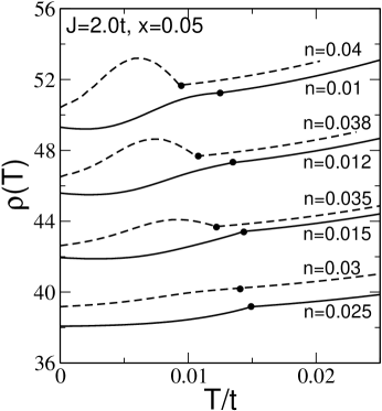
In Figs. 13 and 14 we show our calculated resistivity for GaMnAs samples. We use the parameters corresponding to GaMnAs: dielectric constant , hole effective mass , impurity density , and the magnetic coupling constant 120 meV nm3. Fig. 13 shows normalized resistivity as a function of temperature for several values of hole density. In Fig. 13 there are two independent sources of temperature dependence in our calculated resistivity — one source is the energy averaging defined in Eq. (19) and the other is the explicit temperature dependence of the finite temperature RPA screening function . Since the Fermi temperature is much higher than the critical temperature () the screening function is weakly temperature dependent above the critical temperature (unpolarized state). Thus the decrease of the resistivity above with increasing temperature arises from the thermal energy averaging. This is a well-known high-T effect of ionized impurity scattering in semiconductors: decreases with increasing due to the thermal averaging. As density decreases this effect is enhanced. In the ferromagnetic polarized state (), as the temperature decreases from , the screening length increases until all the holes are polarized. In this temperature range we find a strong temperature dependent resistivity. This strong temperature dependence arises from the low temperature screening function and the change of the carrier densities of the each subband. When all the carriers are polarized (i.e. at low density and temperature) the screening function is almost independent of temperature and the resistivity is also therefore temperature independent. The interplay between the screening length and the down spin (–) carrier density gives rise to the minimum of the resistivity in the low density regime. The decrease of the scattering time due to the fast increase of the down spin density overwhelms the increase of the scattering time due to the decrease of the screening length, producing the non-monotonic behavior for and in Fig. 13. But in the high density regime, where the spins are not fully polarized even at low , screening is the dominant effect on the temperature dependent resistivity. As the density increases the relative low temperature resistivity, , decreases until the holes are partially polarized. The change of screening wave vector is larger in this case, leading to the monotonically increasing in the regime.
In Fig. 14 we show our calculated resistivity as a function of temperature for two hole densities (a) 0.1 and (b) 0.2 with finite temperature RPA screening function. The temperature dependence of the impurity (i.e. Mn) moment magnetization as well as the hole spin polarization is given in the insets, which is calculated using the Weiss molecular mean-field theory for delocalized carriers dassarma03 . Note that the hole gas is almost fully spin polarized upto at low density, but at higher density the holes are partially polarized even at . The bottom insets show the calculated temperature dependence of the finite temperature screening wave vector . At high density the screening wave vector changes by 6% when the temperature increases from zero to due to the partial polarization of the holes at . But at low density the decrease of the screening wave vector is about 20%. In the metallic GaMnAs samples the change of the resistivity when the temperature goes from to zero is about 20% in good agreement with our calculation. Similarly the observed decrease of for also arises naturally in our theory as a consequence of thermal averaging. Thus, the temperature dependence of the resistivity in the metallic DMS samples may be arising almost entirely from the temperature dependence of screening and thermal averaging in the charged impurity scattering.
VI discussion
We have developed in this work two complementary theories for understanding DMS transport properties. Our work establishes that DMS transport, even in ideal intrinsic circumstances, is rather complex, and depends sensitively on many system parameters including the exchange coupling, the magnetic impurity density, the carrier density, the temperature, the band parameters of the parent semiconductor (e.g. effective mass, etc.), and the details of the charged impurity distribution (and therefore compensation). Given such a complex parameter space, it is not meaningful to try to develop quantitative transport theories at this early stage of the subject since all the intrinsic parameters may not be known. We therefore focus in this work on developing a comprehensive qualitative theoretical description which emphasizes general broad features of how various parameters affect DMS transport behavior. As such we have concentrated in this work on understanding temperature and carrier density dependence of dc resistivity in a model DMS system, keeping primarily the extensively studied Ga1-xMnxAs system in mind. Even for GaMnAs, the transport data for various values of Mn concentration () cover much too broad a range of behavior for a unified and coherent theoretical description. For example, low (and sometimes large) Mn concentrations ( and sometimes ) are known to lead to insulating transport behavior usually attributed to a disorder-driven metal-insulator (Anderson) localization. We neglect all localization effects in our theory. The localized GaMnAs regime in all likelihood requires its own characteristic theoretical description such as the bound magnetic polaron percolation theory kaminski1 whose transport properties kaminski2 have recently been theoretically analyzed.
Even without the disorder-induced strong localization complications, neglected completely in this work, we face the formidable difficulty of using the semiconductor valence/conduction band (the valence band for GaMnAs, where the carriers mediating the ferromagnetic interaction are holes) or the magnetic impurity induced impurity band (i.e. Mn induced d-band in the fundamental band gap of GaAs) picture for describing the carrier dynamics. The precise nature (i.e. valence band versus impurity band) of the DMS carriers is still a controversial issue although it is likely that at the very high doping densities (e.g. Mn density in GaMnAs) of DMS interest the impurity band overlaps strongly with the valence band (i.e. forms the tail of the valence band), and therefore, the distinction between the valence and the impurity band picture is not a real qualitative difference. Our DMFT theory, presented in sections II-IV of this paper, clearly shows that in the strong exchange coupling () regime the impurity band picture applies whereas in the weak-coupling regime (), the valence band picture applies. It is possible that GaMnAs belongs to the intermediate coupling regime (), where it may be more appropriate to think of the holes to be residing in the extended tail of the valence band, presumably with an enhanced effective mass compared with the GaAs valence band hole mass. Such a coupled impurity-valence band picture of GaMnAs is consistent with recent optical spectroscopy measurements hirakawa ; singley , but more experimental work is needed to settle this question.
The theoretical strength of our DMFT description is that, being a nonperturbative technique, it can handle both strong-coupling and weak-coupling regimes, and our results presented in Figs. 6 – 10 of this paper show qualitative difference between the strong-coupling regime () with an impurity band well-separated from the semiconductor band and the intermediate-coupling regime () with only band-tailing and no separate impurity band formation. Temperature, carrier density, and impurity concentration all play qualitatively important roles in determining the dc transport properties within DMFT, and sorting out the details with respect to experimental results may be extremely difficult.
The weakness of DMFT is that it can only include spin-disorder scattering (controlled by ) and Mn impurity induced local potential scattering (controlled by ) effects on transport properties. As such it leaves out the most important scattering mechanism which may be operational in real samples, namely scattering by charged impurities which is often the most important resistive scattering process in heavily doped semiconductos below the room temperature (or the optical phonon scattering regime which may well be above the room temperature). The reason DMFT is unable to account for charged impurity scattering is that the Coulombic impurity potential is long ranged, and DMFT by construction is a local theory. Thus, rewriting our starting Hamiltonian (Eq. 1) more completely we have
| (26) |
where is the carrier-charged impurity interaction and is the carrier-carrier (i.e. hole-hole in GaMnAs) interaction. In principle, the terms (i.e. , ) within the square bracket are parts of the , but it is important to appreciate their considerable (perhaps even dominant) importance in determining the dc transport properties. To include the charged impurity scattering effects on transport, we use the highly successful and robust semiclassical Boltzmann transport theory to DMS systems assuming a mean-field approach where the long-range Coulomb impurity potential arising from (assuming random impurity scattering) is screened by the polarization bubble diagrams arising from . This type of Boltzmann transport theory is extremely successful in describing semiconductor transport properties dassarma . We note that our DMFT and Boltzmann transport theories are complementary – DMFT treats the spin disorder and the local potential scattering associated with Mn dopants and Boltzmann theory treats the scattering by screened charged impurity scattering.
The magnetic DMS properties enter the Boltzmann theory only indirectly through the carrier spin polarization calculations. Spin disorder scattering is not explicitly included in the Boltzmann theory although it is straightforward to do so. Our Boltzmann theory manifests nontrivial interplay among temperature dependent screening, temperature dependent spin polarization (i.e. spin up-down carrier densities), and thermal energy averaging, leading to temperature dependent resistivity (Figs. 13 and 14) that are rather similar to experimental observations Matsukura98 in GaMnAs. Based on this qualitative similarity we conclude that much of GaMnAs DMS transport is dominated by screened charged impurity scattering with spin disorder scattering playing only a rather minor quantitative role. Recently, Lopez-Sancho and Brey brey2 have come to a very similar conclusion for GaMnAs transport properties.

Before concluding we now discuss our theoretical results in light of the existing DMS transport data. Although there are some experimental transport data in other DMS systems (most notably InMnAs with qualitatively similar behavior to GaMnAs), truly extensive and reliable transport dataMatsukura98 are available only for Ga1-xMnxAs (in the regime) DMS samples. Even for this well-studied system, experimental transport results are problematic, and have considerable spread in the sense that nominally “identical” GaMnAs samples (i.e. same nominal carrier density and Mn concentration made in the same growth run) may have different and transport properties. This situation is improving as sample quality and processing (e.g. annealing) techniques improve, but experimental DMS transport properties are still not robust in a quantitative way. This is of course very understandable given the very large parameter space (i.e. exchange coupling, hole density, Mn concentration, defects and impurities, compensation, band structure parameters, etc) that DMS transport depends on. With these serious caveats we show in Fig. 15 a schematic depiction of the generic experimental observation for in GaMnAs for various hole densities. At high hole density the system shows “metallic” behavior for with increasing somewhat with upto , and then decreasing slowly for . Even the optimally doped most “metallic” GaMnAs is, however, at best a bad metal with mobilities of the order of 10 with where is the transport mean free path. It is important to realize that DMS transport is always extremely highly resistive due to the very large amount of impurities and defects invariably present in the low temperature MBE process needed for producing homogeneous GaMnAs samples. Thus, from the perspective of heavily doped semiconductors, although the DMS systems may be above the Mott limit (i.e. the carrier density in the Mott metallic range), they are close to being Anderson insulators due to strong disorder effects. As hole density decreases the system eventually becomes an insulator at low enough carrier densities (the top curve in Fig. 15), with decreasing monotonically increasing .
Two generic features of Fig. 15 are: (a) a peak (or a kink) in near , and (2) the slow decrease of for . Both of these generic features of as well as the “metallic” high-density behavior are qualitatively (perhaps even semi-quantitatively) well-explained by our Boltzmann theory approach including only scattering by ionized impurity scattering. This is apparent by comparing Fig. 15 with Figs. 14 and 13 where our Boltzmann theory results are shown. Physically, the increasing with () arises from the decreasing strength of screening due to the interplay of two independent and competing physical effects: Temperature induced suppression of screening and spin polarization (i.e. the spin polarization decreasing with increasing temperature) induced enhancement of screening with increasing temperature. As explained in Sec. V the competition between these two effects depend on the carrier density, leading to some weak non-monotonicity in for . In this screening picture, the resistivity peak or cusp at arises from the ferromagnetic to paramagnetic transition which affects screening as the carrier density of states (which is inversely proportional to the screening length) changes from one in the fully spin polarized state to two in the fully paramagnetic phase. Thus, even without any spin disorder scattering effects, just screened ionized impurity scattering by itself will give rise to the peak or the kink in at . We believe that spin disorder scattering, which also produces a kink at (see, for example, Figs. 7 and 9), play only a minor role in the resistivity “maximum” at in optimally metallic GaMnAs with most of the peak structure arising from the screening properties of ionized impurity scattering. The second generic experimental feature in Fig. 15, the slow decrease of for , cannot be explained at all by spin disorder scattering since spin disorder should remain large in the paramagnetic system () and certainly should not decrease with increasing . Our Boltzmann theory provides a natural explanation (Figs. 13 and 14) for the decreasing as arising from the energy averaging of the relaxation time (Eq. 19), i.e., decreases with increasing simply because the holes move “faster” at higher temperatures (i.e. increasing kinetic energy with increasing ). This decreasing with increasing () also shows that our neglect of phonon scattering in the transport theory is a valid approximation since phonon effects will always increase with increasing . will increase again when phonon scattering starts dominating over ionized impurity scattering at much higher temperatures. The relative lack of importance of phonon scattering in DMS systems arises from their very strong charged impurity resistive scattering effects as reflected in very small sample mobilities.
VII conclusion
In this paper we investigate the transport properties of the diluted magnetic semiconductors using dynamical mean field theory and Boltzmann transport theory. We have shown that the resistivity depends strongly on the system parameters, i.e., exchange coupling, carrier density, doping, and temperature. The resistivity drop with decreasing temperature in the ferromagnetic state can be partially explained by the screening theory for metallic samples. The parameter dependence of the resistivity contains important information about the physics of diluted magnetic semiconductors. We find that in the strong exchange coupling regime the spin disorder scattering and the formation of the bound state in the impurity band compete to produce an unusual behavior in the temperature dependent resistivity. We also show that in the weak coupling regime the occupation of the minority spin band is critical to the scattering mechanisms, and substantially reduces the resistivity because the repulsive interaction between local moments and “wrong-spin” carriers suppresses the carrier amplitude at the impurity site, reducing the effective carrier-spin coupling. Our Boltzmann transport theory for charged impurity scattering is good qualitative agreement with the existing DMS experimental data, showing that transport in DMS GaMnAs system may very well be dominated primarily by screened ionized impurity scattering (with spin disorder scattering playing only a minor secondary role), at least for the optimally doped metallic GaMnAs samples. We have completely neglected detailed band structure complications (e.g. spin-orbit coupling in the valence band) in our theory. These effects are certainly very important, but our interest in this paper is the development of a conceptually coherent qualitative theory for DMS transport identifying the main transport mechanisms, and as such we have neglected all nonessential complications.
ACKNOWLEDGEMENT
We thank DARPA and US-ONR for support.
References
- (1) H. Ohno, Science 281, 951(1998); J. Magn. Magn. Mater. 200, 110(1999).
- (2) H. Ohno et al., Appl. Phys. Lett 69, 363 (1996); A. Van Esch et al., Phys. Rev. B56, 13103(1997).
- (3) F. Matsukura et al., Phys. Rev. B57, R2037(1998); S.J. Potashnik, K.C. Ku, S.H. Chun, J.J. Berry, N. Samarth, and P. Schiffer, Appl. Phys. Lett. 79, 1495 (2001); Sh.U. Yuldashev, H. Im, V.Sh. Yalishev, C.S. Park, T.W. Kang, S. Lee, Y. Sasaki, X. Liu, and J.K. Furdina, Appl. Phys. Lett. 82, 1206 (2003).
- (4) M. Reed et al., Appl. Phys. Lett. 79, 3473 (2001); N. Theodoropoulou, A. F. Hebard, M. E. Overberg, C. R. Abernathy, S. J. Pearton, S. N. G. Chu, and R. G. Wilson Phys. Rev. Lett. 89, 107203 (2002)
- (5) S. Das Sarma, Am. Scientist 89, 516 (2001); I. Zutic, J. Fabian, and S. Das Sarma, Rev. Mod. Phys. 76, 323 (2004).
- (6) S. Das Sarma, E. H. Hwang, and A. Kaminski, Phys. Rev. B67, 155201 (2003); Solid State Comm. 127, 99 (2003).
- (7) A. Oiwa, S. Katsumoto, A. Endo, M. Hirasawa, Y. Iye, H. Ohno, F. Matsukura, A. Shen, and Y. Sugawara, Solid State Comm. 103, 209 (1997).
- (8) K. Hirakawa, A. Oiwa, and H. Munekata, Physica E 10, 215 (2001).
- (9) P. G. de Gennes and J. Friedel, J. Phys. Chem. Solids, 4, 71 (1958); M. E. Fisher and J. S. Langer, Phys. Rev. Lett. 20, 665 (1968).
- (10) See e.g. Colossal Magnetoresistive Oxides, Y. Tokura, ed. (Gordon and Breach, 1999).
- (11) A. Georges, G. Kotliar, W. Krauth, and M. J. Rozenberg, Rev. Mod. Phys 68, 13 (1996).
- (12) A. Chattopadhyay, S. Das Sarma, and A. J. Millis, Phys. Rev. Lett. 87, 227202 (2001).
- (13) E. H. Hwang, A. J. Millis, and S. Das Sarma, Phys. Rev. B65, 233206 (2002).
- (14) Y. Shaprira and R. L. Kauta, Phys. Rev. B10, 4781 (1974); C. Haas, Phys. Rev. 168, 531 (1968);P. Kuivalainen, Phys. Stat. Sol. B227, 449 (2001).
- (15) M.P. Lopez-Sancho and L. Brey Phys. Rev. B68, 113201 (2003).
- (16) D. J. Priour, Jr., E. H. Hwang, and S. Das Sarma, Phys. Rev. Lett. 92, 117201 (2004).
- (17) S. Sanvito, P. Ordejón, and N. A. Hill, Phys. Rev. B63, 165206(2001).
- (18) T. Pruschke, D. L. Cox, and M. Jarrel, Phys. Rev. B47, 3553 (1993).
- (19) A. Chattopadhyay, A. J. Millis, and S. Das Sarma, Phys. Rev. B61, 10738 (2000).
- (20) N. Furukawa in Physics of Manganites, edited by T. Kaplan and S. Mahanti (Plenum, New York, 1999).
- (21) E. J. Singley, R. Kawakami, D. D. Awschalom, and D. N. Basov, Phys. Rev. Lett. 89, 097203 (2002); Phys. Rev. B 68, 165204 (2003).
- (22) A. Kaminski and S. Das Sarma, Phys. Rev. Lett. 88, 247202 (2002).
- (23) A. Kaminski and S. Das Sarma, Phys. Rev. B 68, 235210 (2003).
- (24) S. Das Sarma and E. H. Hwang, Phys. Rev. B69, 195305 (2004).