Simulation of quantum dead-layers in ferroelectric tunnel junctions
Abstract
In this letter, we simulate electronic transport through a metal-ferroelectric-metal tunnel junction by use of a nonequilibrium Green’s function approach. We show that quantum effects such as Friedel oscillations lead to deviations from the Thomas-Fermi screening model. As a consequence, we predict a bistable resistive switching effect, depending on the polarization state of the ferroelectric tunnel barrier.
pacs:
XXXThe finite penetration depth of the electric field in a metallic system leads to considerable corrections to the electronic properties of a metal-insulator-metal tunneling structure Kiejna and Wojciechowski (1996). For example, Mead Mead (1961) observed a deviation from the classical geometric capacitance arising from the electric field penetration into the metal electrodes. This finding was explained theoretically by Ku and Ullman Ku and Ullman (1964), as well as Simmons Simmons (1965), by modeling the total capacitance as a sum of a (geometric) dielectric capacitance and electrode capacitance contributions (due to the finite field penetration). Black and Welser extended this approach to high-k materials (for example BaSrxTi1-xO3) Black and Welser (1999). In general, the field penetration effect is pronounced in capacitors and tunnel junctions containing ultrathin insulator films with a high dielectric permittivity. In addition, field penetration was also noticed in the context of finite size effects of complex oxide ferroelectric capacitors Mehta et al. (1973); Junquera and Ghosez (2003); Dawber and Scott (2002); Dawber et al. (2003). The finite screening length furthermore leads to uncompensated ferroelectric charge layers at metal-ferroelectric interfaces under short circuit conditions. First-principles calculations by Junquera and Ghosez predicted ferroelectric instabilities in SrRuO3/BaTiO3/SrRuO3 heterostructures with a tunnel barrier thickness even down to nm. (In fact, recent experiments on Lead compound oxides demonstrated ferroelectricity in ultrathin films Tybell et al. (1999); Fong et al. (2004)). In all examples, the field penetration in the metal electrodes was described on the basis of the Thomas-Fermi screening length Kiejna and Wojciechowski (1996).
In this letter, we show that quantum interference effects such as Friedel oscillations Kiejna and Wojciechowski (1996) lead to deviations from the semiclassical Fermi-Thomas screening within a metal-insulator-metal tunnel junction. Recently, we presented the concept of a ferroelectric tunnel junction (FTJ) Kohlstedt et al. (2002); Contreras et al. (2003) based on a metal-ferroelectric-metal (MFM) layer sequence, consisting of two (semi-) metals separated by an ultrathin ferroelectric layer as visualized in the inset of Fig. 1(a).
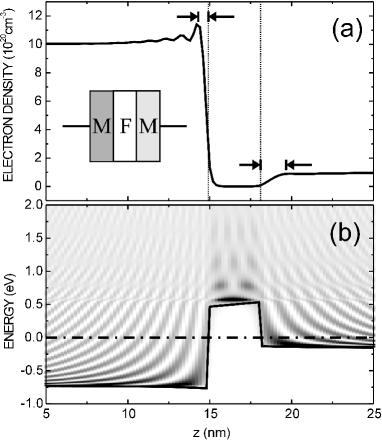
In order to simulate the IV characteristics of the FTJ, a non-equilibrium Green’s function approach has been used Indlekofer and Malindretos (2000); Indlekofer et al. (2002); Schäfer and Wegener (2002). The employed empirical tight-binding one-band formulation constitutes a good approximation for the description of conduction band electrons inside the ferroelectric tunnel barrier and the (semi-) metallic electrodes. Within this framework, Coulomb charging effects are accounted for in terms of a self-consistent Hartree-potential. Polarization charges at the two interfaces of the ferroelectric material are implemented as charged mono-layers. (For simplicity, we assume a mono-domain polarization state with a polarization vector perpendicular to the junction plane. The device structure is translationally invariant within the grown layers.) An applied bias voltage is implemented as a difference in the local Fermi-energies of the two reservoirs.
In the following, we will discuss an idealized case of an MFM structure, assuming an effective electron mass of and a dielectric constant of throughout the device. The ferroelectric tunnel barrier of nm and eV height (with interface polarization charges of cm-2) is surrounded by two (semi-) metallic contact regions with electron concentrations of cm-3 and cm-3, respectively. (Of course, the chosen parameters have to be adjusted to the individual experimental device structure.)
Fig. 1(a) shows the simulated electron contration under zero bias conditions (short circuit case). Due to the wave-nature of the electron, Friedel oscillations arise within the electrode regions in the vicinity of the tunnel barrier (clearly pronounced in the left contact). The oscillation period is given by the Fermi wavelength divided by two ( nm in the l.h.s. reservoir) Kiejna and Wojciechowski (1996). As an important consequence, quantum mechanically determined partially depleted regions close to the tunnel barrier arise (see arrows in Fig. 1(a): nm and nm), in contrast to the abrupt electron concentration drop in the classical case. We refer to this phenomenon as a ”quantum dead-layer” (analogous to a conventional dead-layer Drougard and Landauer (1959) which also introduces a non-screening and non-ferroelectric region at the metal-insulator interface). Within the semi-metallic electrode on the r.h.s., the depleted region is further extended due to band-bending, varying with the applied voltage. In Fig. 1(b), the corresponding self-consistent potential profile is shown (solid line) with a grayscale plot for the local density of states (LDOS). One can clearly identify the polarization charge at the interfaces of the ferroelectric tunnel barrier in terms of a kink in the continuous part of the potential and a tilted barrier potential due to the resulting depolarization field. The LDOS plot reveals the wave-properties of the electron: Firstly, standing wave patterns result from reflections at the tunnel barrier, giving rise to the Friedel oscillations with a quantum dead-layer. Secondly, multiple reflections within the barrier region yield resonances in the higher energy region. (Latter may become relevant for hot-carrier injection conditions.) Furthermore, within the reservoir on the l.h.s., a shallow triangular quantum well arises, which is responsible the screening charge.
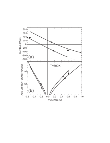
The local electric field within the ferroelectric barrier as a function of the applied voltage is shown in Fig. 2(a). Here, an intrinsic coercitive field of kV/cm has been assumed, resulting in transition voltages of approximately V and V. The asymmetry stems from the assumed electron concentration asymmetry within the electrodes. Since there is a significant voltage drop within the electrode regions close to the barrier (depleted regions), the external voltage necessary to induce a polarization flip in the ferroelectric material is significantly higher than the intrinsic voltage drop across the barrier. Additionally, in Fig. 2(b), the corresponding current-density vs. voltage characteristics is plotted in a log-scale, revealinge an exponential behavior of the current density which is determined by the tunnel barrier. Depending on the the polarization state and the sign of the applied voltage, the slope in the log-scale varies due to different potential profiles. The bistable IV characteristics could make such an MFM device a possible candidate for a non-volatile memory element. Obviously, the total capacity of the considered device structure will also be affected by the quantum dead-layer and depletion effects discussed above.
In conclusion, we have considered quantum interference effects in ultrathin metal-ferroelectric-metal tunnel junctions. The current-voltage charateristics of an exemplary tunnel structure has been simulated with the help of a nonequilibrium Green’s function formalism. As a result, a bistable resistive switching behavior was predicted.
Acknowledgements.
This work was supported by the the Volkswagen-Stiftung Project Nano-sized ferroelectric hybrids under Contract No. I/77737. The financial support by the Deutsche Forschungsgemeinschaft (DFG) is gratefully acknowledged.References
- Kiejna and Wojciechowski (1996) A. Kiejna and K. F. Wojciechowski, Metal Surface Electron Physics (Elsevier Science Ltd., 1996).
- Mead (1961) C. A. Mead, Phys. Rev. Lett. 6, 545 (1961).
- Ku and Ullman (1964) H. Y. Ku and F. G. Ullman, J. Appl. Phys. 35, 265 (1964).
- Simmons (1965) J. G. Simmons, Appl. Phys. Lett. 6, 54 (1965).
- Black and Welser (1999) C. T. Black and J. J. Welser, IEEE Trans. Electron Dev. 46, 776 (1999).
- Mehta et al. (1973) R. R. Mehta, B. D. Silverman, and J. T. Jacobs, J. Appl. Phys. 44, 3379 (1973).
- Junquera and Ghosez (2003) J. Junquera and P. Ghosez, Nature 422, 506 (2003).
- Dawber and Scott (2002) M. Dawber and J. F. Scott, Jap. J. Appl. Phys. 41, 6848 (2002).
- Dawber et al. (2003) M. Dawber, P. Chandra, P. B. Littlewood, and J. J. Scott, J. Phys.: Condens. Matter 15, 393 (2003).
- Tybell et al. (1999) T. Tybell, C. H. Ahn, and J.-M. Triscone, Appl. Phys. Lett. 75, 856 (1999).
- Fong et al. (2004) D. D. Fong, B. G. Stephenson, S. K. Streiffer, J. Eastman, O. Auciello, P. H. Fuoss, and C. Thompson, Science 304, 1650 (2004).
- Kohlstedt et al. (2002) H. Kohlstedt, N. A. Pertsev, and R. Waser, in Ferroelectric Thin Films X (Material Research Society, 2002), vol. 688, p. 161.
- Contreras et al. (2003) J. R. Contreras, H. Kohlstedt, U. Poppe, R. Waser, C. Buchal, and N. A. Pertsev, Appl. Phys. Lett. 83, 4595 (2003).
- Indlekofer and Malindretos (2000) K. M. Indlekofer and J. Malindretos, WinGreen Simulation Package (Research Centre Jülich, 2000), URL http://www.fz-juelich.de/isg/mbe/wingreen.html.
- Indlekofer et al. (2002) K. M. Indlekofer, E. Donà, J. Malindretos, M. Bertelli, M. Kočan, A. Rizzi, and H. Lüth, phys. stat. sol. (b) 234, 769 (2002).
- Schäfer and Wegener (2002) W. Schäfer and M. Wegener, Semiconductor Optics and Transport Phenomena (Springer-Verlag, 2002).
- Drougard and Landauer (1959) M. E. Drougard and R. Landauer, J. Appl. Phys. 30, 1663 (1959).