Finite bias charge detection in a quantum dot
Abstract
We present finite bias measurements on a quantum dot coupled capacitively to a quantum point contact used as a charge detector. The transconductance signal measured in the quantum point contact at finite dot bias shows structure which allows us to determine the time-averaged charge on the dot in the non-blockaded regime and to estimate the coupling of the dot to the leads.
pacs:
73.21.La, 73.23.HkI Introduction
The charge state of a quantum dot can be read out using a nearby quantum point contact (QPC) as a detector.Field et al. (1993) Real-time readout has been recently demonstrated using radiofrequency single electron transistors Wei-Lu et al. (2003) or QPCs.Schleser et al. (2004); Elzerman et al. (2004) Together with a spin-charge conversion mechanism, this is being considered a candidate for a qubit readout scheme Elzerman et al. (2004) in a future quantum computing device based on coupled quantum dots.Loss and DiVincenzo (1998)
A valuable piece of information about a quantum dot’s characteristics is the knowledge about its coupling to each of the reservoirs. This coupling is determined by the electrostatic barrier forming the constriction and the wave function overlap leading to tunneling. The latter may strongly depend on the quantum state under consideration in the dot, which means that the quantum mechanical tunnel coupling has to be determined for each state individually. In the Coulomb blockade regime, for the case of single-level transport, a fit of a transport peak in the Coulomb blockade regime enables one to extract an effective tunnel coupling where and are the couplings to the source and the drain reservoir, respectively. However, the ratio remains unknown.
In earlier work on finite bias transport Bonet et al. (2002), e.g. in carbon nanotubes,Cobden et al. (1998) it was shown that in principle, the individual coupling to both leads of the dot can be extracted from the current amplitudes at positive and negative bias. Since these considerations make use of a spin blockade effect, however, they apply only to the case of spin degenerate states in the dot, and require an even number of electrons on the dot. In addition, they rely on the absence of cotunneling. Recently, a method was presented Leturcq et al. (2004) to measure the coupling of a dot to its reservoirs for a three-terminal quantum dot.
In the following, we present finite bias measurements of transport through a quantum dot, complemented by simultaneous measurements of the conductance of a nearby, electrostatically coupled QPC used as a charge detector. While the latter allows us to determine the time-averaged charge on the quantum dot even in the non-blockaded regime, the combination of both methods makes it possible to provide qualitative estimates for the quantum mechanical coupling of the dot’s energy levels to each of the two reservoirs.
II Experimental setup
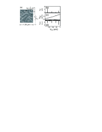
The sample (see Fig. 1(a)) was fabricated using surface probe lithography Held et al. (1999); Lüscher et al. (1999); Nemutudi et al. (2004) on a GaAs/Al0.3Ga0.7As heterostructure, containing a two-dimensional electron gas (2DEG) below the surface as well as a backgate (BG) below the 2DEG. The unstructured 2DEG had a mobility of and an electron density at a BG voltage at .
All measurements were performed in a dilution refrigerator at a base temperature of .
Negative voltages were applied to the surrounding gates (G1, G2, S, D, the latter two also containing the charge detection circuit; see Fig. 1(a)), and to the BG, to reduce the charge on the dot and close its tunnel barriers. A voltage applied to gate P was used to tune the detector QPC to a regime where it is sensitive to the charge on the dot. The QD bias voltage was applied symmetrically (with respect to ground) across the dot between source (S) and drain (D).
Due to the electrostatic coupling of the QPC to the dot, a change in the dot’s charge leads to a modification in the QPC’s confining potential, resulting in a change of its conductance.Field et al. (1993) The latter was measured by applying a dc voltage and measuring the resulting current. Each additional electron on the dot leads via electrostatic interaction to a shift of the QPC conductance’s dependence on gate voltage: , where is the number of electrons on the dot. If we assume that the QPC is tuned to a regime between two conductance plateaux with an approximately constant derivative , then we can subtract as a background and get a signal proportional to the additional charge on the dot: . This technique has recently been applied to investigate the charging behaviour of a double quantum dot.DiCarlo et al. (2004)
In our measurements, in order to avoid the influence of nonmonotonuous drift in , we measured the transconductance as an additional quantity, using a lock-in setup at a frequency of . The voltage was composed of a constant dc voltage, used to tune both the dot’s and the QPC’s chemical potential, and a small ac voltage used to periodically change the chemical potential inside the dot by a small amount (of the order of ). The bias across the QPC was applied symmetrically with respect to , in order to minimize its influence on the chemical potential inside the dot. Figure 1(a) illustrates the QPC related part of the circuit diagram. Figures 1(b)-(d) show the correlations between the three quantities in a simultaneous measurement: at the position of a Coulomb blockade peak in the current through the dot, a kink appears in the QPC’s conductance, corresponding to a change in the dot’s charge by one. In the transconductance , a dip is observed. , being a derivative of the QPC current, differs from only by a constant background and a factor given by the ratio of the corresponding lever arms, . This ratio should depend only weakly on gate voltages. One can therefore obtain the time-averaged charge on the dot by integrating the measured value with respect to , (after subtracting a constant and a weak linear background to compensate for the gate voltage dependence of ) and normalizing the resulting steps to unity.
III Time averaged charge detection
In Fig. 2(a), we present finite bias measurements of the dot’s conductance. From these, estimates for the charging energy and the mean level spacing were extracted. Fig. 2(b) shows a simultaneous measurement of the QPC’s transconductance.
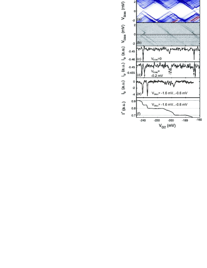
In the transconductance plot, diagonal lines with the same slope as the diamond boundaries in the dot conductance plot are observed, marking a change of the dot’s time-averaged charge. The lines correspond to the alignment of an energy level in the dot with either the source (negative slope) or the drain (positive slope) reservoir, while their intensity contains information about the magnitude of the change in charge.
Figure 2(c) shows the transconductance at low bias. Dips in the signal at the gate voltages of the Coulomb blockade peaks correspond to the change in electronic charge by one elementary charge each. For a finite bias (Fig. 2(d)), the peaks split, illustrating that the time-averaged charge on the dot changes in steps smaller than the unit charge .
These steps in charge can be directly visualized by integrating over the transconductance (Fig. 2(e)-(f)). In order to improve the precision of the charge determination, the transconductance was averaged over a finite bias range prior to numerical integration. A constant (corresponding to the direct coupling between the in-plane gates used for ac excitation and the QPC) and a linear term (corresponding to the gate voltage dependence of ) were then subtracted. To conserve the steepness of the steps near , the individual traces were laterally shifted with respect to each other before averaging. As a consequence, the step corresponding to the second Coulomb peak is broadened, since for this peak the slope of the corresponding lines in Fig. 2(b) is different.
The large steps marked by dashed horizontal lines in Fig. 2(f), corresponding to a change in charge by one elementary charge each, have almost identical height, as one would expect. Charge rearrangements during the measurements, one of which is visible at in Fig. 2(a), might contribute to errors in the numerical integration and thus may lead to small differences in total step height.
To verify the usefulness of the integrated signal as a measure for the mean charge on the dot, we compared the step size related to a single electronic charge for several Coulomb peaks (see Fig. 2(f)) and for different bias ranges between zero and the height of a Coulomb diamond. The difference in step height did not exceed 10 percent if a sufficient number of traces was taken into account to reduce the statistical error. Even in the high-bias regime near the border of the Coulomb-blockaded bias range, where the lines in the transconductance seem to gradually disappear, the integrated transconductance signal gives a good measure of the mean charge, which means that line broadening compensates for the lower amplitude.
IV Estimation of dot-lead coupling: non-degenerate case
From the information about the mean charge in the non-blockaded region, it is possible to extract the coupling of individual states to each lead separately by using a rate equation approach:Beenakker (1991) if a single energy level lies within the (thermally broadened) bias range between the Fermi level of both leads, the mean dwell time of the th electron in the dot is determined by the relative value of the couplings and to both leads. The ’s account for the height of the tunnel barriers , the wave function overlap between the dot and lead, and the density of states inside the leads, which we assume to be constant. The occupation probability of the energy level then becomes
| (1) |
where stands for the energy distribution in the leads (which we assume to be the Fermi distribution) and the indices S and D stand for source and drain, respectively. For a bias voltage and a chemical potential not inside the thermally broadened ranges around the Fermi energies of both leads, we have , , and this expression becomes for (positive bias) and for (negative bias).
Since the non-integer (fluctuating) part of the mean charge on the dot in the level is given by , this connects the integrated transconductance value to the ratio :
| (2) |
Together with the expression for the transport current
| (3) |
it is possible to determine the numerical values of and .
The analysis of the transconductance signal becomes more involved if more energy levels inside the quantum dot are contributing to transport. It is thus preferable to start the analysis in the regime of single-level transport, i.e. . In addition, the maxima in the transconductance signal associated with source and drain alignment of the level must be clearly separable, i.e. . Those two requirements limit the bias range over which the integration of the transconductance peak can be performed on a given data set, especially when excited states are present near the ground state. To apply the method described above, we have to verify that there exists a finite bias range where these conditions are met.
We analyzed the low finite bias regime around three conductance peaks in a range where the system was most stable, for five different magnetic fields applied, to change the shape of the dot’s wave functions and their overlap with the leads. In our analysis, we encounter two qualitatively different situations in the low bias transconductance regime: No branching at zero bias (this section): single line with constant slope crossing the zero bias line, possibly branching at finite bias. Branching at zero bias (degenerate case, discussed in the next section).
An example of the first case is encountered, e.g., at the second peak in Fig. 2(a)/(b) (see detail in Fig. 3(a)), in the low bias regime: near , we observe a broadened line with negative slope in the transconductance, while a similarly broadened, but comparatively weak maximum is measured in the transport current (Fig. 2(a)).
Figure 3(b) shows a schematic representation of Fig. 3(a), illustrating which line corresponds to the alignment of the dot’s chemical potential with source (S) and drain (D). Figures 3(c)-(f) illustrate how coupling and level alignment determine the mean electron number on the dot. Note that in Fig. 3(e), an asymmetrically coupled level can become nearly 100 percent occupied even in the non-blockaded regime.
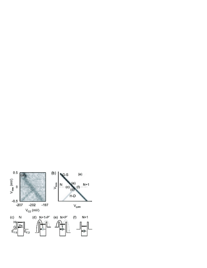
The observation near is compatible with the presence of a single energy level strongly coupled to the source reservoir (leading to enhanced broadening, compared to a Coulomb blockade peak width of purely thermal origin), but extremely weakly coupled to the drain contact. This would explain the observed low zero-bias transport current and the fact that within our measurement resolution, no line with positive slope corresponding to an alignment to the drain contact is observed in the transconductance. At finite negative bias, i.e. once a more symmetrically coupled excited state becomes accessible (see finite bias region around middle peak in Fig. 2(a)), transport is strongly enhanced.
Solving equations 1 and 3 for and yields an upper bound for the ratio of the coupling constants . From the measured value of the transport current in the finite bias regime (averaged over positive and negative bias), we obtain an estimate for , so that both are uniquely determined within the errors mainly resulting from charge measurement uncertainties. In fact, for this very asymmetric case, we might assume that level broadening is caused entirely by the more strongly coupled source lead. The full width at half maximum of the Coulomb peak is of the order , yielding a value for which suggest an even stronger asymmetry .
At finite bias, a splitting of the line in the transconductance is observed, suggesting that an excited state of the dot more symmetrically coupled to both leads governs its mean occupation. Inserting this into a numerical simulation (see below) also yields qualitative agreement with the observed finite bias dot current, which shows a larger step change at the positive than at the negative bias corresponding to the excitation energy.
V Estimation of dot-lead coupling: degenerate case
In a number of cases the lines in the transconductance plot branch at zero bias (leftmost peak in Fig. 2(b), see detail in Fig. 4(a)). This splitting is not compatible with the participation of only one individual single-particle level in transport. At finite positive bias, a further splitting occurs and a line with opposite bias dominates, suggesting predominant coupling towards the source contact.
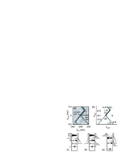
From our transconductance measurements, the mean occupation was determined by integrating over a voltage range in in the transconductance plot, summing over a range of bias voltages to reduce the statistical errors. Normalization was performed by integrating over the whole non-blockaded gate voltage range, summing over the same bias range.
To elucidate the origin of the low bias results (depicted schematically in Fig. 4(b)), we performed analytical calculations using a rate equation approach based on the framework of Beenakker’s theory of sequential electron tunneling.Beenakker (1991)
We assumed that a model involving at least two quasi-degenerate states might describe our findings, and therefore extended equations 1-3 to the case of two degenerate levels, involving four coupling values ( for source and drain; ).
To extract a meaningful result despite the large relative errors in the charge input values, we express the in terms of a global multiplicative factor , the symmetries of each of the two states and the relative weight of the two states , expressed as the ratio of the geometrical averages of their couplings. The resulting simple expressions for the become: , , , .
Using the four charge and transport values at low positive and negative bias as input values, the expressions for current and occupation can be solved for the four new parameters. The numerical values obtained are , , , . This means that one of the two levels has approximately symmetric coupling, while the second is predominantly coupled to the drain contact. This state must therefore have a very asymmetric distribution of the wave function amplitudes to the two reservoir connections, since we learn from the slopes observed in Fig. 2(b) that the dot as a whole predominantly couples to the source reservoir, suggesting an asymmetry in the tunnel barriers themselves. Since the numbers show that the two states have different symmetry properties, the most obvious possibility of a spin pair has to be excluded in this case.
The method described above can be extended to determine the coupling properties of higher energy states by incrementally solving the more intricate rate equations involving a larger number of levels, using measurements at higher bias and the previously calculated values as an input. The major advantage of this procedure is that it correlates data measured at a constant value of the controlling gate, changing only the bias of the dot: due to spectral scrambling, the information obtained in this way is rarely accessible by comparing successive Coulomb peaks.
We perfomed this analysis using numerical calculations based on the same aforementioned rate equation approach. Even though the input values include already a certain error, some qualitative statements can be derived: the most important one concerns the feature visible in Fig. 4(a), showing a change in slope in the right positive bias line occuring at finite bias. The fact that the line with positive slope is discontinued is not compatible with the presence of a single excited state. Again, two quasi-degenerate states are necessary to explain the scenario observed. The coupling of these two states has to be asymmetric with predominant coupling to the source contact. The measurements are compatible with the two states having identical coupling values, leaving open the possibility of a spin pair. Fig. 4(b) shows a numerical simulation using the values from the analytical calculations above for the two lower states (responsible for the low bias behaviour). The remaining were determined numerically by iteratively comparing experiment and simulation.
The resolution of our charge detector is limited: all the transconductance measurements presented above were performed in a regime in which the QPC’s conductance remained between and . Slight changes in the lithographic pattern for future structures will permit us to approach the tunneling regime, resulting in a tenfold increase in charge sensitivity and a more precise determination of the mean charge and the coupling strengths.
VI Conclusions
We have demonstrated how a QPC charge detector for a nearby quantum dot can be used to extract information about the average charge in the non-blockaded finite-bias regime. Together with the conductance measurement through the dot itself, this allows us to extract qualitative and quantitative information about the coupling of single energy levels to the source and drain reservoirs.
Financial support from the Schweizerischer Nationalfonds is gratefully acknowledged.
References
- Field et al. (1993) M. Field, C. G. Smith, M. Pepper, D. A. Ritchie, J. E. F. Frost, G. A. C. Jones, and D. G. Hasko, Phys. Rev. Lett. 70, 1311 (1993).
- Wei-Lu et al. (2003) Wei-Lu, Zhongqing-Ji, L. Pfeiffer, K. W. West, and A. J. Rimberg, Nature 423, 422 (2003).
- Schleser et al. (2004) R. Schleser, E. Ruh, T. Ihn, K. Ensslin, D. C. Driscoll, and A. C. Gossard, Appl. Phys. Lett. 85, 2005 (2004).
- Elzerman et al. (2004) J. M. Elzerman, R. Hanson, L. H. W. van Beveren, B. Witkamp, L. M. K. Vandersypen, and L. P. Kouwenhoven, Nature 430, 431 (2004).
- Loss and DiVincenzo (1998) D. Loss and D. P. DiVincenzo, Phys. Rev. A 57, 120 (1998).
- Bonet et al. (2002) E. Bonet, M. M. Deshmukh, and D. C. Ralph, Phys. Rev. B 65, 045317 (2002).
- Cobden et al. (1998) D. H. Cobden, M. Bockrath, P. L. McEuen, A. G. Rinzler, and R. E. Smalley, Phys. Rev. Lett. 81, 681 (1998).
- Leturcq et al. (2004) R. Leturcq, D. Graf, T. Ihn, K. Ensslin, D. D. Driscoll, and A. C. Gossard, Europhys. Lett. 67, 439 (2004).
- Held et al. (1999) R. Held, S. Lüscher, T. Heinzel, K. Ensslin, and W. Wegscheider, Appl. Phys. Lett. 75, 1134 (1999).
- Lüscher et al. (1999) S. Lüscher, A. Fuhrer, R. Held, T. Heinzel, K. Ensslin, and W. Wegscheider, Appl. Phys. Lett. 75, 2452 (1999).
- Nemutudi et al. (2004) R. Nemutudi, M. Kataoka, C. J. B. Ford, N. J. Appleyard, M. Pepper, D. A. Ritchie, and G. A. C. Jones, J. Appl. Phys. 95, 2557 (2004).
- DiCarlo et al. (2004) L. DiCarlo, H. J. Lynch, A. C. Johnson, L. I. Childress, K. Crockett, C. M. Marcus, M. P. Hanson, and A. C. Gossard, Phys. Rev. Lett. 92, 226801 (2004).
- Beenakker (1991) C. W. J. Beenakker, Phys. Rev. B 44, 1646 (1991).