Extraordinary optical transmission without plasmons: the s-polarization case
Abstract
It is shown that extraordinary optical transmission through perforated metallic films is possible for s-polarization. Although surface plasmons do not exist for this polarization, their role can be played by a surface wave sustained by a thin dielectric layer on top of the metallic film. This confirms that the existence of a surface wave, whatever its nature, is the responsible for the extraordinary optical transmission phenomenon.
pacs:
78.66.Bz, 42.79.Dj, 71.36.+c, 73.20.MfAlready in the original experimental paper Ebbesen , surface plasmons were pointed to as the reason of extraordinary optical transmission (EOT) through two-dimensional (2D) arrays of subwavelength holes in optically thick metallic films. The initial EOT theoretical models Schroter ; Porto ; Treacy ; Tan ; Lalanne ; Collin considered 1D arrays of subwavelength slits. This is a much simpler system where both polarizations (s and p) are decoupled. Moreover, the modes supported by the slits in p-polarization are very different from those supported by the holes Popov , the former not having cutoff wavelength. Despite these limitations, the models distinctly showed that EOT only occurs for p-polarization (magnetic field parallel to the slits), the only one for which surface plasmons are possible. Later Luis , better suited 2D models also supported the surface plasmon picture. Shortly after, it was realized that simulations with perfect metals also displayed EOT and, since flat perfect conductors do not sustain surface plasmons, this was unexpected. Such behavior has been recently cleared up Pendry ; FJ by showing that corrugation (with grooves, holes, or dimples) of perfect metals gives rise to surface electromagnetic modes with a plasmon-like behavior (so called spoof plasmons) for the p-polarization case. Thus, all mentioned instances of EOT in metals, and in other systems, e.g., photonic crystals Moreno1y2 , are mediated by surface waves.
Let us now solely consider the 1D s-polarization case. As said, plasmons in real metals are not possible for this polarization. An analysis similar to FJ shows that surface structuring of perfect metals does not produce s-polarized spoof plasmons, the reason being the different kind of boundary conditions. Since s-polarization surface waves are excluded for metals, it seems that EOT is restricted to p-polarization. In this paper we demonstrate that addition of a thin dielectric film on the metal interface creates a surface wave that allows for EOT in the “wrong” s-polarization case.
The considered system consists of a thin metallic film embedded in vacuum, pierced by a periodic slit array with periodicity . The film thickness is , and the slit width is , unless otherwise explicitly stated. The possibility of supporting a surface wave is achieved by adding a dielectric layer ( is taken for proof of principle purposes) on the metal film, with thickness . Almost all results presented here correspond to s-polarization (electric field parallel to the slits). We are interested in the subwavelength regime, i.e., the slits are narrow and the modes guided inside the slits are evanescent. Notice that in spite of the geometric similarity to the case considered in Christ , here we are in a very different regime: the transmittance of our system without dielectric film is negligible, whereas in Christ transmittance without film is nearly 1 because the slits are very wide. For the sake of simplicity our models consider perfect conductors in most of the paper, which is undoubtedly appropriate for microwave frequencies. Nevertheless, in order to show that the mechanism is also valid for the optical regime, a more realistic dispersive and absorptive dielectric constant , standing for the frequency, is employed towards the end of the paper. All simulations have been carried out with the multiple multipole (MMP) method Christian .
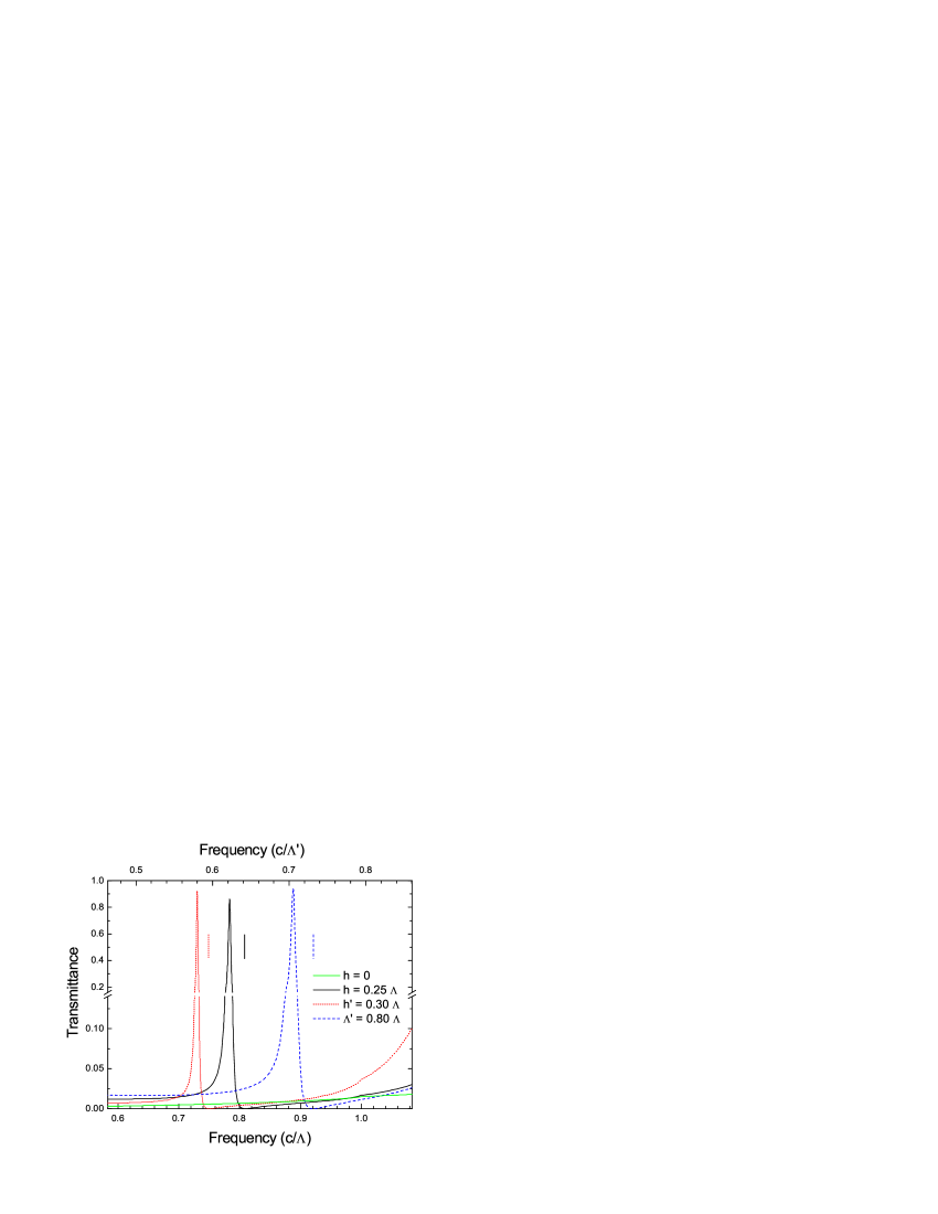
The green and black lines in Fig. 1 represent the 0-order diffracted transmittance for orthogonal incidence in the cases without dielectric layer () or with it (), respectively. Without dielectric film the transmittance is nearly zero (less than 2%), but EOT is observed as soon as a thick enough film is added (transmittance reaches 86%). The black line displays a resonant feature including a maximum and a minimum. The spectral position of this feature depends on the geometric parameters and in the usual way in EOT. Namely, if we consider the unperturbed surface wave guided by the dielectric film on top of a continuous metallic substrate (i.e., without slits), we have checked that the resonant feature is close to the frequency that satisfies the condition
| (1) |
being the modal wavelength of the unperturbed surface wave. Below we will be more precise about the relation between the position of the maximum, , minimum, , and . Since the surface wave dispersion relation, , depends on the film thickness and dielectric constant , the position of the resonant feature depends on , , and . Figure 1 also displays an example varying and keeping the other parameters unaltered (, red line), and another example varying and keeping the other parameters unaltered (; , , , blue line). Equation (1) gives the location of the resonant feature in all cases (see the short vertical segments in Fig. 1). Notice that, in a sense, the system considered here is more akin to the original 2D hole array studied in Ebbesen than the first 1D theoretical models in p-polarization Schroter ; Porto ; Treacy ; Lalanne ; Collin . The reason is that the slits are subwavelength and therefore, for s-polarization, the slit modes are evanescent as it also happens in the hole array case. In Ebbesen the position of the resonant frequencies depends on the substrate dielectric constant, whereas here this role is played by (and/or ).
If the frequencies and in Fig. 1 are confronted with the frequency , one realizes that is always very close to . Such a circumstance sparked a controversy for the original p-polarization EOT models about the role of the surface plasmon Cao . Since it was argued that the surface plasmon is only responsible for the minimum in transmission and therefore it plays a negative role in EOT. In the original 1D models of EOT, plasmons lay very close to the light line (for the considered frequency regime), and therefore the resonance was very close to the Rayleigh anomaly, further obscuring the subject. In the system considered here the surface wave can be tailored so that the mode is not close to the light line and the analysis is easier. This is clear in Fig. 1 where the resonance is far from the Rayleigh anomaly, occurring for (where is the speed of light in vacuum).
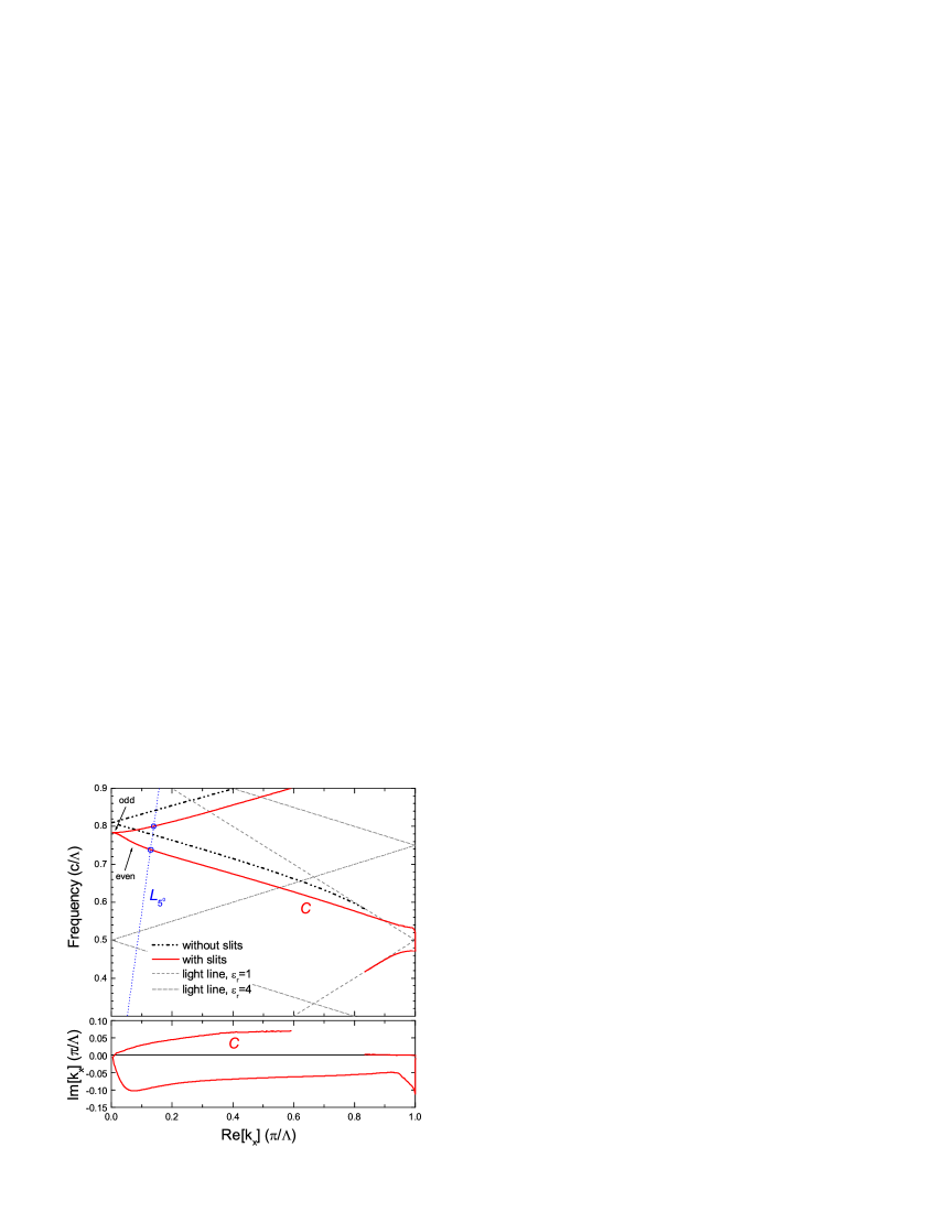
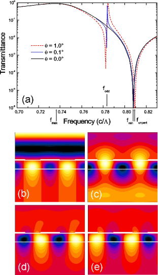
To shed some light on this issue we have computed the complex band structure of our system (Fig. 2). In order to better separate the frequencies of the various modes involved, the following parameters were chosen: , , and , i.e., the slit is now wider than previously, but it remains in the subwavelength regime. The band structure is obtained by searching for the poles of the scattering amplitude in the complex plane (see Moreno3 for details; similar diagrams are found in other contexts Brundrett ). From Fig. 2 it is possible to infer the frequencies of the transmission maxima as follows. For a given incidence angle , resonances occur at the intersection of the dispersion relation curve , and the line , given by . In fact, this is only approximately correct because the poles lie in the complex plane, and since is real it cannot intersect a complex . However, whenever comes close to , a resonance shows up in the transmission spectrum. The case is exceptional: as can be observed in Fig. 2, in this case there is an intersection of and at . But the mode at this frequency has odd parity, it cannot couple with the even excitation, and therefore it does not appear in the normal incidence spectrum. This is verified in Fig. 3(a) that renders the transmittance spectrum for normal and slightly off-normal incidences. The resonant feature at associated to the odd mode disappears for normal incidence. The broad maximum seen in this graph at arises because comes close to at this frequency (symmetry not preventing the coupling in this case). To summarize, the existence of the surface wave is responsible for both the maximum and the minimum occurring in the transmittance spectrum for normal incidence (this resonant feature is a typical Fano resonance profile Genet ). Therefore it should not be concluded that the surface wave is detrimental for the EOT but rather responsible for it (remind that in the absence of the dielectric film, the spectrum is absolutely featureless in the considered range). Let us point out that at [Fig. 3(b)] the field in the slits is very close to zero, and therefore the global field is very similar to the unperturbed surface wave; this is why (notice, however, that ). On the other hand, at [Fig. 3(c)] the signature of the unperturbed surface wave can be clearly recognized, but the stronger coupling to radiation modifies the pattern and consequently shifts the position of the maximum. The modal field at can be inferred from Figs. 3(d) and (e).
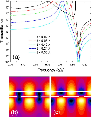
At the resonance a high transmittance (but lower than 1) is obtained. It was already observed in Krishnan that the EOT can be boosted for symmetric structures. For the configuration presented here, it is possible to achieve unit transmittance by considering a symmetric structure, i.e., with identical dielectric films on the top and the bottom of the metallic film (the slits are also filled with dielectric, but they are still subwavelength in the interesting frequency range). Such a situation is shown in Fig. 4. For symmetry reasons, now four modes are expected, which are even or odd with respect to both the vertical and the horizontal symmetry planes. In a similar way to the previously considered case, only two of them [even with respect to the vertical symmetry plane, see Fig. 4(b) and (c)] show up in the transmittance spectrum for normal incidence, but now with 100% transmittance. When the metal film thickness is increased, the two maxima become closer, merge, and then the maximum transmittance decreases exponentially as the metal thickness grows (similar behavior was found in the 2D hole array case).
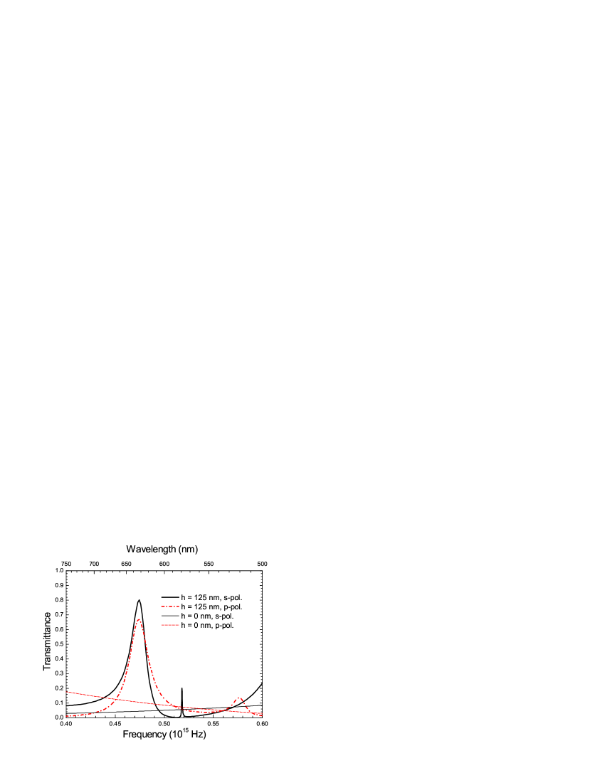
All our simulations up to this point have considered perfect metals. The explained mechanism is nevertheless valid for the optical range, where the perfect metal model breaks down. Let us therefore conclude with a Drude metal model (appropriate for the optical regime). The considered parameters are the following: , , , (in a symmetric configuration, i.e., dielectric films at both sides), and . The background is vacuum and the metal’s dielectric constant is , with , and , appropriate for gold. As Fig. 5 shows (thick black line), the maximum transmittance (80.5%) is now lower than in the previous examples. This is due to the weaker evanescent coupling (the metallic layer is thicker) and to the absorption losses. The metal supports surface plasmons and therefore EOT for p-polarization is expected. One would naively expect that this structure is very sensitive to polarization. However, the parameters can be chosen so that the p and s-polarization resonant peaks occur at the same frequency and with similar transmittances (thick red line). Thus, a highly polarization-anisotropic structure can deliver a very polarization-isotropic response.
In conclusion, we have shown that EOT depends uniquely on the existence of a surface mode and a corrugation allowing the coupling of the incident wave to the surface mode. EOT for s-polarization (i.e., without plasmons) has been demonstrated, the nature of the wave and its polarization being irrelevant for the occurrence of the phenomenon.
Funded by the Spanish MCyT under contracts MAT2002-01534 and MAT2002-00139, and the EC under projects FP6-2002-IST-1-507879 and FP6-NMP4-CT-2003-505699.
References
- (1) T. W. Ebbesen et al., Nature (London) 391, 667 (1998).
- (2) U. Schröter and D. Heitmann, Phys. Rev. B 58, 15419 (1998).
- (3) J. A. Porto, F. J. García-Vidal, and J. B. Pendry, Phys. Rev. Lett. 83, 2845 (1999).
- (4) M. M. J. Treacy, Appl. Phys. Lett. 75, 606 (1999).
- (5) W.-C. Tan, T. W. Preist, and R. J. Sambles, Phys. Rev. B 62, 11134 (2000).
- (6) P. Lalanne et al., J. Opt. A: Pure Appl. Opt. 2, 48 (2000).
- (7) S. Collin et al., Phys. Rev. B 63, 033107 (2001).
- (8) E. Popov et al., Phys. Rev. B 62, 16100 (2000).
- (9) L. Martín-Moreno et al., Phys. Rev. Lett. 86, 1114 (2001).
- (10) J. B. Pendry, L. Martín-Moreno, and F. J. García-Vidal, Science 305, 847 (2004).
- (11) F. J. García-Vidal, L. Martín-Moreno, and J. B. Pendry, J. Opt. A: Pure Appl. Opt. 7, S97 (2005).
- (12) E. Moreno, F. J. García-Vidal, and L. Martín-Moreno, Phys. Rev. B 69, 121402(R) (2004); Photonics and Nanostructures 2, 97 (2004).
- (13) A. Christ et al., Phys. Rev. Lett. 91, 183901 (2003).
- (14) C. Hafner, Post-Modern Electromagnetics, (John Wiley and Sons, Chichester, 1999).
- (15) Q. Cao and P. Lalanne, Phys. Rev. Lett. 88, 057403 (2002).
- (16) E. Moreno, D. Erni, and C. Hafner, Phys. Rev. B 65, 155120 (2002).
- (17) D. L. Brundrett et al., J. Opt. Soc. Am. A 17, 1221 (2000).
- (18) C. Genet, M. P. van Exter, and J. P. Woerdman, Opt. Commun. 225, 331 (2003).
- (19) A. Krishnan et al., Opt. Commun. 200, 1 (2001).