High-Performance Carbon Nanotube Field-Effect Transistor with Tunable Polarities
Abstract
State-of-the-art carbon nanotube field-effect transistors (CNFETs) behave as Schottky barrier (SB)-modulated transistors. It is known that vertical scaling of the gate oxide significantly improves the performance of these devices. However, decreasing the oxide thickness also results in pronounced ambipolar transistor characteristics and increased drain leakage currents. Using a novel device concept, we have fabricated high-performance, enhancement-mode CNFETs exhibiting or -type unipolar behavior, tunable by electrostatic and/or chemical doping, with excellent OFF-state performance and a steep subthreshold swing ( mV/dec). The device design allows for aggressive oxide thickness and gate length scaling while maintaining the desired device characteristics.
Index Terms:
carbon nanotube, Schottky barrier, field-effect transistor, dopingI Introduction
Since the discovery of carbon nanotubes in the early 1990s[1, 2], the field has witnessed an immense growth. Due to the small diameter ( nm), nanotubes are ideal candidates to study one-dimensional electrical transport phenomena, even at room temperature. In particular, single-walled carbon nanotubes, which consist of a single layer of graphene sheet wrapped up to form a seamless tube[3], possess exceptional electrical properties, such as high current carrying capability[4] and excellent carrier mobility[5]. Both theory and experiments have demonstrated that these tubes can be either metallic or semiconducting, depending on the chirality of their atomic structure with respect to the tube axis. Using semiconducting nanotubes, carbon nanotube field effect transistors (CNFETs) have been first realized and reported in Refs.[6] and [7]. These early CNFETs, however, showed poor device characteristics. Since then, remarkable progress has been made to improve the performance of CNFETs by approaches such as: (1) reducing the gate oxide thickness[8]; (2) adopting high- dielectrics for the gate oxide[9, 10, 11]; (3) using electrolyte as the gate [12, 13]; (4) reducing contact resistance by choosing proper contact metals[14] or post-process treatments[15]. These techniques have significantly advanced CNFET devices to exhibit characteristics rivaling those of state-of-the-art Si-based MOSFETs. With the scaling limit of conventional CMOS in sight[16], carbon nanotubes show great promise among the materials investigated so far for post-Si technology.
Most CNFETs studied so far have adopted a back-gate, top-contact geometry (see [17] and [18] for a review), as shown in Fig. 1(a). In this back-gate configuration, the nanotubes are dispersed or grown on a conducting substrate covered by an insulating layer. Two metal contacts are deposited on the nanotube to serve as source and drain electrodes, while the conducting substrate is the gate electrode in this three-terminal device. This CNFET structure, albeit simple, has been extensively studied to provide invaluable insights and understanding of fundamental properties of nanotubes. However, these CNFETs are found to possess several unfavorable features that severely constrain their usefulness in vital applications such as CMOS-like circuits. In order to address the disadvantages of a simple back-gated CNFET, in this report we present a novel device concept for CNFETs. In particular, our device design is capable of producing pure - and/or -type CNFETs with improved OFF-state performance and abrupt switching behavior close to theoretical limits.
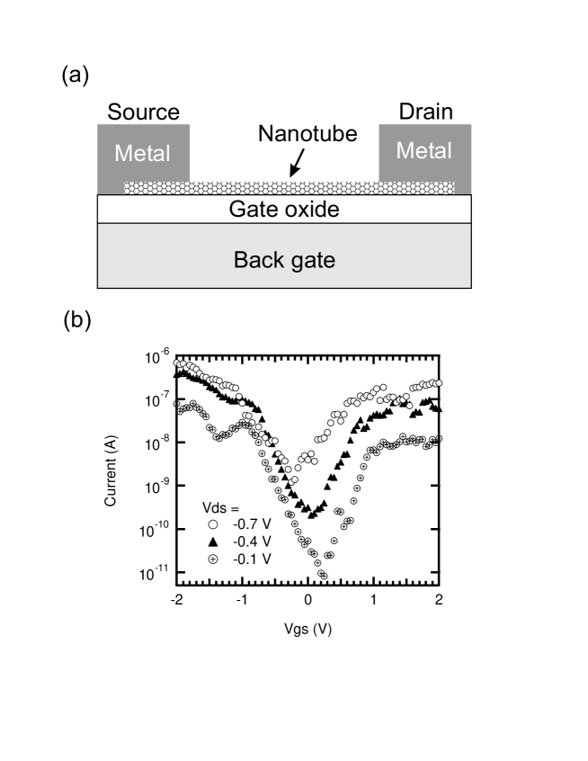
First we review important electrical characteristics of the back-gated CNFET as shown in Fig. 1(a). The understanding of operation principles and physics of this device is indispensable in order to obtain desired functionality and further improvements. Figure 1(b) shows the subthreshold characteristics, the drain current measured as a function of gate voltage , of a back-gated CNFET for different drain voltages (). For all the measurements presented in this report, the source electrode is grounded. This CNFET device is fabricated on a heavily -doped Si substrate covered by a thin layer (10-nm thick) of thermally-grown SiO2 with titanium (Ti) contacts. In Fig. 1(b), two distinct features are observed. First, as the gate voltage increases from negative values, the current decreases, reaching a minimum value of , and A for , -0.4, and -0.7 V, respectively, and then rises again, exhibiting an ambipolar transistor characteristic. Second, as the drain bias becomes more negative, the minimum current increases exponentially and the gate voltage corresponding to this minimum current shifts to more negative values, showing a strong -dependent .
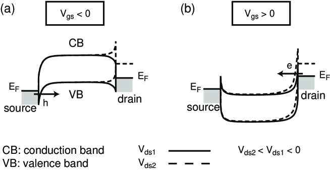
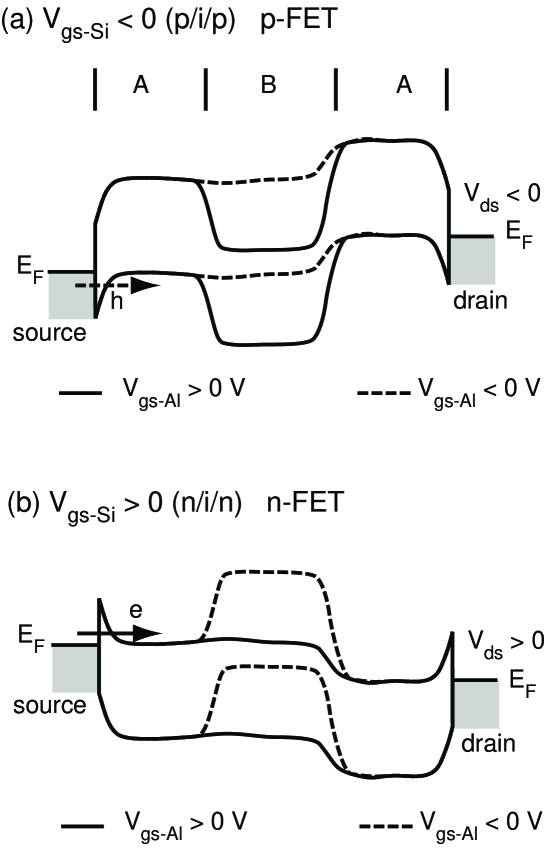
In order to understand the results of Fig. 1(b), Figures 2(a) and (b) depict schematic band diagrams of a CNFET for negative and positive , respectively. We note that, different from a conventional MOSFET, switching of a CNFET is dominated by the modulation of Schottky barriers (SBs) formed at the nanotube/metal contacts[19, 15, 10, 20]. As indicated in Figs. 2(a) and (b), at sufficiently negative and positive gate voltages, Schottky barriers are effectively thinned to enable hole injection () from the source and electron injection () from the drain contact into the nanotube, respectively. Compared to the tunneling phenomena in a 3D bulk device, this tunneling current in CNFETs can be quite significant because a barrier width ( depletion length ) as small as a couple of nanometers can be obtained for a ultra-thin body object, such as a nanotube, when thin gate dielectrics are used[21]. We also notice that in Fig. 2, there is little band bending in the nanotube body because the carrier mean-free-path in nanotubes can be as long as nm even at room temperature [22, 23], so that carrier transport is nearly ballistic for the nanotube channel length ( nm) considered here. In Fig. 1(b), the left and right current branches with respect to the minimum current are therefore contributions by hole and electron currents, and are referred to in the following as - and -branches, respectively. At the minimum current , the hole current is equal to the electron current. Since the electron current is due to the tunneling at the drain contact, the -branch exhibits a much stronger dependence than the -branch (see Fig. 2 for two different ), resulting in a shift of the -branch as a function of and a strongly -dependent as shown in Fig. 1(b). All these electrical characteristics of CNFETs have been studied previously, and detailed discussions can be found in Refs.[20, 24, 25].
Both simulations and experimental results have shown that the switching performance of CNFETs, measured by the inverse subthreshold slope , and the ON-state current can be improved by decreasing the gate oxide thickness[8, 10, 26, 11, 9]. However, the enhanced gate control in a CNFET always also results in a higher with a more pronounced dependence as explained before[24]. In addition, from application’s point of view, both and -type transistors with unipolar characteristics are required for CMOS-like logic circuits, while thin-oxide CNFETs are usually ambipolar, as shown in Fig. 1(b). In order to advance nanotubes for future transistor technology, these disadvantages associated with vertical scaling have to be overcome. We have recently demonstrated the conversion of an ambipolar CNFET to a unipolar transistor using a partially-gated structure where a trench is created near one of the contacts to eliminate drain leakage[27]. However, it was also found that this partially-gated structure results in a reduced ON-current and is not suitable for scaling to small lateral lengths due to fringing field impacts.
In this report, we present a novel device concept for CNFETs using dual gates to eliminate ambipolar characteristics and create pure - and/or -type devices with excellent OFF-state performance and a steep subthreshold swing. This is achieved by a combination of electrostatic and/or chemical doping along the tube channel. By introducing a distinct or band structure along the nanotube (where , and represent an -doped, a -doped, and an undoped (intrinsic) nanotube segment, respectively), we have successfully modified the switching mechanism of our CNFET[28]. Instead of contact switching by modulating Schottky barriers, our device operates by varying the band potential in the middle portion of the nanotube body, called bulk-switching, and achieves an inverse subthreshold slope mV/dec, the smallest value reported for CNFETs to date. Furthermore, this unique device structure affords aggressive gate length scaling without deteriorated device performance.
II Novel Dual-Gate CNFET Design
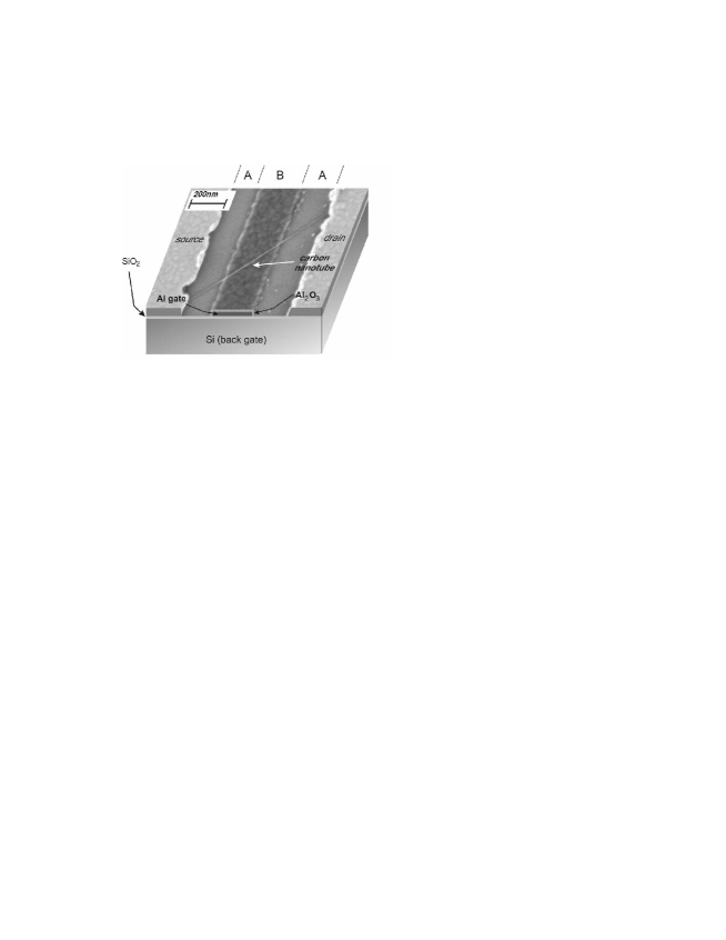
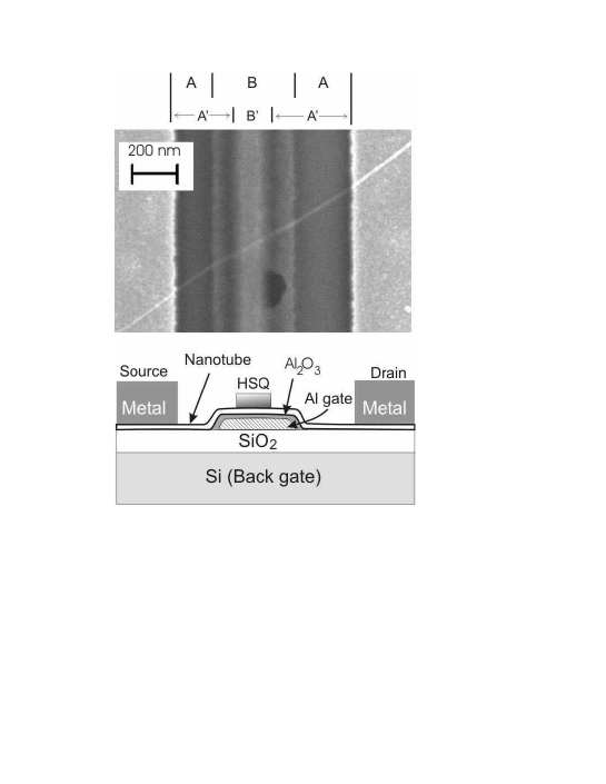
Figure 3 shows the SEM image as well as the device cross-section of a CNFET with the proposed dual-gate structure[28]. Different from the back-gated CNFET shown in Fig. 1(a), the dual-gate CNFET possesses an additional Al gate electrode placed underneath the nanotube between the source and drain contacts. To fabricate the dual-gate CNFET, the Al gate (20-nm thick and -nm wide) is first deposited on a -doped Si substrate covered with 10-nm-thick SiO2, followed by the oxidation of Al metal in moisturized oxygen at C for 1.5 hours to form a thin layer of Al2O3 (). Both C-V and ellipsometry measurements of the Al2O3 layer indicate an oxide thickness of about 4 nm, in agreement to the result reported in Ref. [9]. Nanotubes produced by laser ablation [29] with an average diameter of nm are then spun onto the substrate from solution. Finally, source/drain contacts made of Ti are deposited on the nanotube, each with a spacing of nm relative to the Al gate. For the following discussions, the Al gate region is denoted as region B, and the area between the Al gate and the source/drain contacts are denoted as regions A (see Fig. 3).
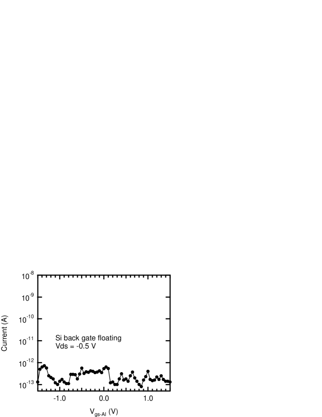
In our design, the Al gate is the primary gate that governs the electrostatics and the switching of the nanotube bulk channel in region B, while the Schottky barriers at the nanotube/metal contacts are controlled by the Si back gate (substrate), which also prevents the electrostatics in region A from being influenced by the Al gate. It was previously observed that carrier injection at the contacts may still be modulated by a middle gate due to fringing field impacts[11, 27]. To verify that the Schottky barriers at the contacts are not affected by the Al gate voltages in our design, Figure 4 shows the measured current as a function of Al gate voltage when the Si back gate is kept floating. We find that our device is always OFF with a low current in the noise level ( pA), independent of , indicating an insignificant impact of the Al gate fields at the contact regions. The result in Fig. 4 implies that our CNFET can operate as a bulk-switched transistor rather than an SB-CNFET since the switching using the Al gate does not impact the contact Schottky barriers.
CNFETs with potential profiles similar to our device have been previously fabricated by using one or more middle gates on top of the nanotube[22, 11, 32]. In those CNFETs, the nanotube is sandwiched between the top gate(s) and the back gate, and the back gate field still contributes to the electrostatics inside the nanotube, resulting in a lower efficiency of the top gate when the back gate is kept at any constant voltage[33]. In contrast, the nanotube potential of region B in our design is exclusively determined by the Al gate because the Al metal layer screens the field from the Si gate, giving rise to an ideal switching behavior. Another important advantage of our design is the possibility of introducing a well-defined chemical doping profile along the nanotube to further tailor transistor characteristics (see Sec. II-B), while no chemical doping profile can be easily introduced in a completely top-gated CNFET.
II-A Electrostatic Doping Effect
In this section we present electrical characteristics of our dual-gate CNFETs at various gate voltage ( and ) configurations. In particular, we utilize electrostatic doping effects in CNFETs to eliminate ambipolar characteristics in an SB-CNFET and to obtain a bulk-switched transistor possessing a tunable polarity ( or ), steep subthreshold swing, excellent OFF-state performance, and suppressed dependence[34]. This is achieved by a distinct or band profile in our dual-gate CNFET.
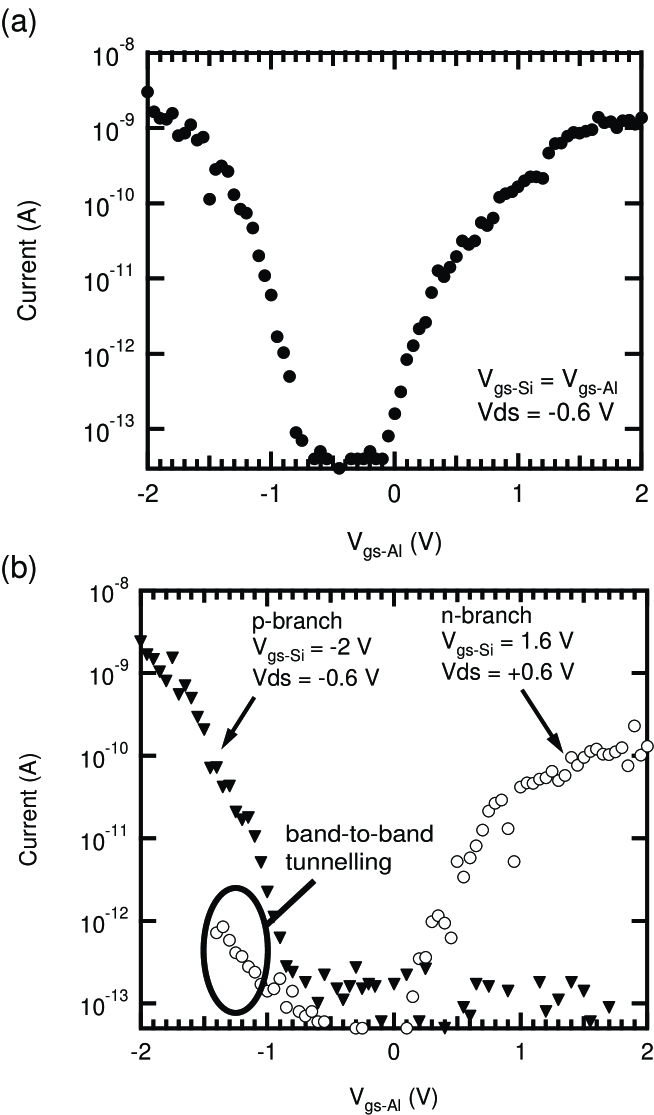
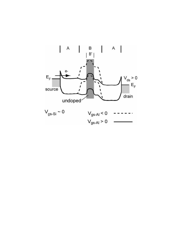
Figure 5(a) shows the subthreshold swing of a dual-gate CNFET at V when the two gate voltages are equal (). In this gate voltage configuration, the device is essentially equivalent to a standard back-gated CNFET as shown in Fig. 1(a), and the switching behavior is mainly determined by the Schottky barriers at the contacts, resulting in the expected ambipolar behavior. In Fig. 5(a), the OFF-current is below our instrument sensitivity level ( A)[36]. The dual-gate CNFET possesses drastically different subthreshold characteristics ( measured as a function of ) when the Si gate voltage is kept constant. As shown in Fig. 5(b), the same dual-gate CNFET exhibits clear and -type unipolar properties for V () and +1.6 V (), respectively. In Fig. 5(b), positive (+0.6 V) and negative (-0.6 V) drain voltages are used for -type and -type branches, respectively, in order to illustrate regular and -FET device operations. This -FET () and -FET () behavior of the dual-gate CNFET can be understood by the schematic band diagrams shown in Figs. 6(a) and (b), respectively. For a sufficiently negative (or positive) Si gate voltage, the Schottky barriers are thinned enough to allow for hole (or electron) tunneling from the metal contacts into the nanotube channel, and regions A become electrostatically doped as -type (or -type), resulting in a (or ) band profile that allows only hole (or electron) transport in the nanotube channel. The dual-gate CNFET is switched ON and OFF by varying the Al gate voltage that alters the barrier height for carrier transport across region B. In this configuration, regions A serve as extended source and drain, and our device operates in a fashion similar to a conventional MOSFET through bulk-switching in region B. We note that for Si MOSFETs, transistors with electrically-induced source/drain regions have been fabricated by using additional side gates [30], and our dual-gate structure is reminiscent of the straddle-gate Si MOSFETs demonstrated by Tiwari et al [31].
The results in Fig. 5(b) are in drastic contrast to the ambipolar behavior of the same device shown in Fig. 5(a), proving the successful elimination of ambipolar characteristics and the first experimental demonstration of controlling the CNFET polarity by means of electrostatic effects. It is interesting to note the -FET branch in Fig. 5(b) exhibits a non-monotonic behavior with the current rising for V, as indicated by the circle in Fig. 5(b). This feature is due to band-to-band tunneling that occurs when the two gate voltages are different enough such that the valence band in region B is higher than the conduction band in regions A (or vice versa). Further discussion of this band-to-band tunneling phenomenon is reported elsewhere[38].
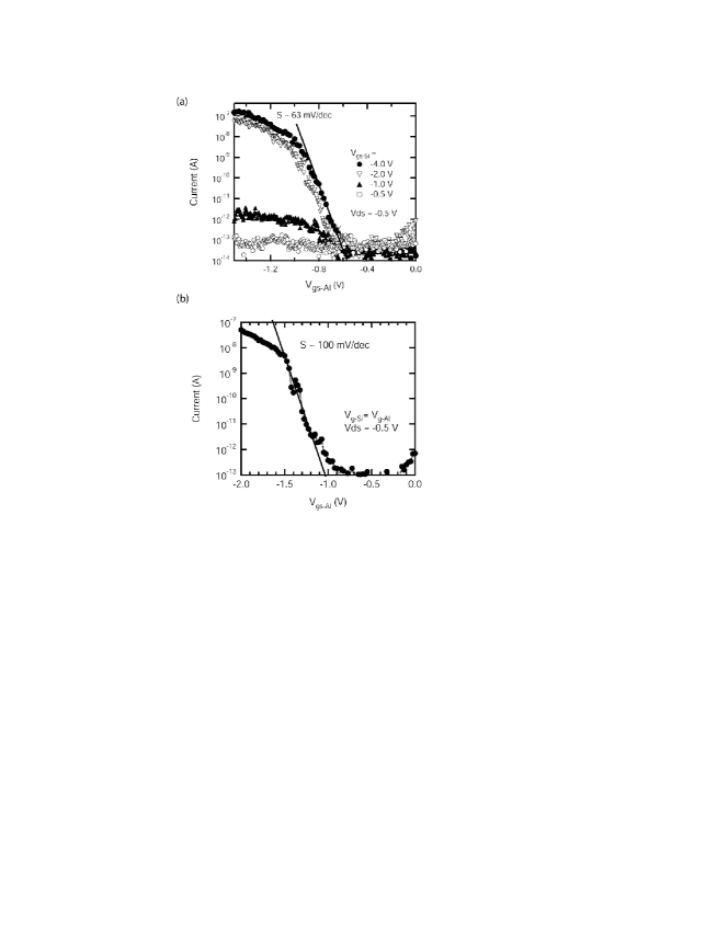
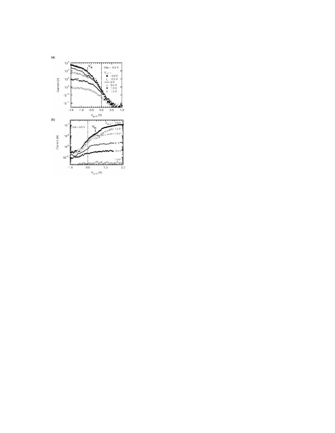
In our dual-gate CNFETs, the Si back gate plays an important role in determining the type of majority carrier and the device ON-current. In order to study the impact of the Si gate voltage on the device performance, Figure 7(a) shows the subthreshold characteristics of a dual-gate CNFET for different Si back gate voltages , with particular emphasis on the -FET branches (). We first note that for V, the ON-current is relatively low because the current is limited by the carrier injection at the Schottky barriers rather than the barrier in region B. For V, in particular, is independent of and the device is essentially OFF for the entire range, indicating the Schottky barrier at the contact prohibits carrier emission for this Si gate voltage. As becomes more negative, the Schottky barrier becomes thinner to facilitate hole injection, giving rise to a higher ON-current. At sufficiently negative ( V), the device operates as an enhancement-mode -FET with a negative threshold voltage and an inverse subthreshold slope mV/dec. We note that this value is the smallest slope reported for CNFETs to date, and is close to the theoretical minimum value of mV/dec attainable for conventional MOSFETs at room temperature (where , , and are the Boltzmann constant, temperature, and electron charge, respectively). In comparison, the same device possesses mV/dec when operated as an SB-CNFET with (see Fig. 7(b)). The results indicate that in addition to the elimination of ambipolar characteristics, a steeper subthreshold swing can also be obtained in our devices due to bulk-switching enabled by the distinct dual-gate design. The nearly-ideal value (63 mV/dec) measured for our dual-gate CNFET suggests a gate efficiency close to 1, which is made possible by the dual back gate design that allows exclusive Al gate control in region B. We further note that in addition to the factors that affect the inverse subthreshold slope for conventional MOSFETs, the value of our dual-gate CNFETs also depends on tunneling properties at the Schottky barriers, as explained in the following.
In the vicinity of the Schottky barriers in regions A, the carrier energy distribution is proportional to the product of , where is the tunneling probability through the Schottky barrier and is the Fermi-Dirac distribution in the metal at temperature . As carriers travel away from the contact, inelastic scattering processes such as electron-phonon interaction will thermalize the carrier distribution back to the equilibrium distribution characterized by the ambient temperature , which is the important parameter in deriving the theoretical value of . However, at low fields, the carrier mean-free-path in CNFETs can be as long as half a micrometer and the transport is essentially ballistic over the entire region A ( nm). Without an effective mechanism [39] to relax the non-equilibrium carrier energy distribution, the carriers arriving at the barrier in region B possess the same distribution as , which can, in principle, deviate significantly from a well-tempered Fermi-Dirac distribution if the tunneling probability is highly energy-dependent. Since tunneling through a Schottky barrier always favors higher energy carriers, the effective temperature of the carrier distribution is higher than the lattice temperature [41], causing a larger value than . Therefore, from the aspect of device performance, a Schottky barrier with constant () is important not only for a high ON-current, but also essential to obtain an inverse subthreshold slope close to 60 mV/dec at room temperature.
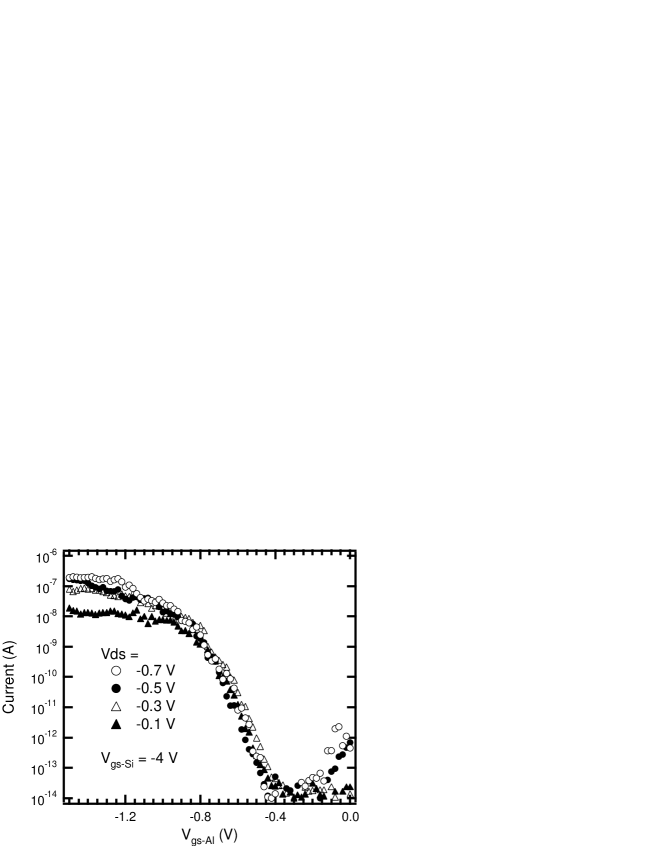
We have also studied the dependence of our device performance, as shown in Fig. 8 for the measured subthreshold characteristics of a dual-gate CNFET at different drain voltages. In Fig. 8, the Si back gate is always kept at -4 V, and the device exhibits -FET characteristics. Compared to the results in Fig. 1(b), the subthreshold swing of the dual-gate CNFET exhibits a much weaker dependence on the drain voltage . The dual-gate CNFET possesses a very low fA, and is almost independent of . This dramatic improvement of OFF-state performance for dual-gate CNFETs is not unexpected because the minority carrier injection from the drain electrode is effectively eliminated by the distinct (or ) band profile in our design (see Fig. 6).
By using a novel dual-gate structure, we have successfully modified the switching mechanism of a CNFET from Schottky barrier modulation to bulk-channel switching, resulting in a unipolar transistor with tunable polarity, excellent subthreshold slopes, and drastically improved OFF-state.
II-B Tuning via Chemical Doping
In the previous section, we have demonstrated CNFETs with improved performance due to a distinct (or ) potential profile along the nanotube by means of electrostatic doping in selected areas (i.e. regions A). By varying the Si back gate voltage, the polarity of the dual-gate CNFET can be readily tuned. The role of the Si back gate, in principle, can be replaced by introducing proper chemical dopants into regions A in order to achieve the same band bending profile. The use of chemical dopants in regions A is attractive because the device can be operated with the back gate grounded () or ultimately without the presence of any back gate, which is essential for high frequency applications to minimize parasitic capacitances. Controlled -type chemical doping of nanotubes has been accomplished previously by using alkali metals or air-stable polymers to create -type transistors[42, 43, 44, 45, 46, 47] and devices[48]. However, in those devices, gating always occurs over the entire nanotube. Based on the dual-gate CNFET design, next we discuss our results on chemical doping in conjunction with electrostatic doping. In particular, -type chemical dopants are used here to obtain an doping profile along the nanotube.
In order to obtain a chemical doping profile along the tube, a resist layer consisting of HSQ is patterned on top of the Al gate area of a dual-gate CNFET. HSQ (Hydrogen SilsesQuioxane) is a negative resist for e-beam lithography, and is compatible with our chemical doping processes for nanotubes. Figure 9 shows the SEM image and the schematic cross-section of a dual-gate CNFET patterned with a layer of HSQ resist. The HSQ layer protects the nanotube segment (region B’ in Fig. 9) from being influenced by chemical dopants, so that a (or ) chemical doping profile can be obtained with respect to regions A’ and B’. In our design, the Al gate and the HSQ layer permit independent electrostatic and chemical doping profiles along the tube channel.
After the HSQ patterning, Figure 10(a) shows measured vs. of a dual-gate CNFET (Ti/Pd contact) at different prior to any chemical doping treatment[49]. We note that this device operates as a -FET even for , suggesting that this CNFET was unintentionally -doped during the fabrication process[11]. However, Figure 10(a) also points out an important fact which is that the nanotube segment in region B’ is not subject to this unintentional -doping because the CNFET is still in the OFF state at V. Therefore, this CNFET possesses a doping profile due to the unintentional -doping effect after the HSQ patterning. The device is then dipped in an ethanol solution containing 25wt% of PEI for 4 hours, followed by an ethanol rinse. Here we use PEI (polyethylene imine), an -type dopant for nanotubes[43], to demonstrate chemical doping effects in our devices. Figure 10(b) shows the measured subthreshold characteristics of the same CNFET after PEI doping, exhibiting a drastically different behavior from that of the original device shown in Fig. 10(a). The clear -FET characteristics for V shown in Fig. 10(b) indicate successful -FET to -FET conversion by doping regions A’ with PEI. One important feature observed in Figs. 10(a) and (b) is that both -FET and -FET devices before and after PEI doping operate as enhancement-mode transistors with threshold voltages of about -0.7 V and +0.4 V, respectively. This is due to the and chemical doping profile enabled by the HSQ resist layer. Without our distinct doping profile, the threshold voltage would shift with increasing doping level, resulting in a depletion-mode transistor at high doping levels[46].
The operation of the dual-gate CNFET with a chemical doping profile can be understood by the band structures depicted in Fig. 11. We note that since the area covered by HSQ resist (region B’) is narrower than the Al gate (region B), there exists an additional band bending within region B where both the Al gate and the chemical dopants are effective. This additional step in the potential profile has little effect on the transistor performance because the switching behavior is mainly determined by the total barrier height rather than the detail structure of the barrier. Band-to-band tunneling currents, on the other hand, may be substantially suppressed because of this step-like band structure in region B.
III Simulation and Discussion
Last, we present simulation results for our dual-gate CNFETs. In the simulation, we consider a CNFET consisting of a nanotube connected to two semi-infinite source/drain metallic contacts, forming Schottky barriers. The dual-gate structure is explicitly taken into account by three gate segments between the contacts, and is characterized by lengths and for regions A and B, respectively. The charge in and the current through the CNFET is calculated self-consistently using the non-equilibrium Green’s function formalism together with a modified 1D Possion equation. A quadratic dispersion relation is assumed in the conduction and valence band. Further details regarding the simulation can be found elsewhere[50].
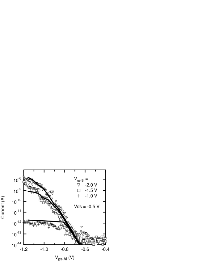
Figure 12 shows both measured and simulated subthreshold characteristics of a dual-gate CNFET (without chemical doping) at different Si back gate voltages[51]. In the simulation, we assumed a nanotube energy gap of 1.0 eV[52] and a Schottky barrier height eV for holes. In Fig. 12, the simulated current as a function of Al gate voltages exhibits excellent agreement with measured data over a wide range of for various Si back gate voltages. In particular, both experiment and simulation yield an inverse subthreshold slope close to 60 mV/dec for sufficiently negative values, confirming the bulk-switching phenomena in our devices. It is noteworthy that as varies, the simulated curves also show good quantitative agreements with experimental data in terms of . The ON-current decreases with increasing because the Schottky barriers at the contact limit the maximum current through the device. The height of the Schottky barrier is determined by the nanotube band gap and the work function of the contact metal. It is expected that by using nanotubes of larger diameters and choosing proper metals for contact electrodes (e.g. Pd), the Schottky barriers can be effectively lowered to achieve an ON-current as high as 25 A [23]. The agreement between experiment and simulation results is encouraging because it not only marks the quality of the model used here, but also provides compelling evidence for the operation concept of dual-gate CNFETs.
Since the regions A of our dual-gate CNFET resembles the extended source and drain in a conventional MOSFET structure, the switching speed of the dual-gate CNFET is mainly determined by the active gate in region B. For high-frequency applications, this active gate length of region B determines the transit time for an electron/hole travelling from source to drain. Therefore, although the entire length between the metal source/drain contacts is , it is , rather than , that is the critical parameter in terms of lateral scaling to improve performance. In order to minimize parasitic capacitances for high-frequency applications, we have also demonstrated that the Si back gate in regions A can be replaced by using chemical dopants, although future studies are needed to quantify the correlation between the doping level and the obtained Fermi level shift.
IV Conclusion
In conclusion, we have fabricated CNFETs with a novel dual-gate structure in order to achieve a distinct or doping profile along the nanotube. The or doping scheme, obtained by electrostatic and/or chemical doping effects, eliminates the ambipolar characteristics and, for the first time, creates pure or -type enhancement-mode CNFETs with a controllable polarity for thin gate oxides. Compared to previous SB-CNFETs where the Schottky barriers dominate the switching behavior, these dual-gate CNFETs are bulk-switched devices, showing the steepest subthreshold slope reported to date. The good agreement between experiment and simulation further corroborates the novel device operation concept of the dual-gate structure.
Acknowledgement
The authors thank Zhihong Chen, Marcus Freitag, and Jia Chen for valuable discussions, and Bruce Ek for metal deposition and expert technical assistance.
References
- [1] S. Iijima and T. Ichihashi, “Single-shell carbon nanotubes of 1-nm diameter,” Nature(London), vol. 363, pp. 603–605, 1993.
- [2] D. S. Bethune, C. H. Kiang, M. S. Devries, G. Gorman, R. Savoy, J. Vazquez, and R. Beyers, “Cobalt-catalized growth of carbon nanotubes with single-atomic-layerwalls,” Nature, vol. 363, pp. 605–607, 1993.
- [3] M. S. Dresselhaus, G. Dresselhaus, and Ph. Avouris, Carbon nanotubes: synthesis, structure, properties, and applications. Berlin: Springer-Verlag, 2001.
- [4] Z. Yao, C. L. Kane, and C. Dekker, “High-field electrical transport in single-wall carbon nanotubes,” Phys. Rev. Lett., vol. 84, pp. 2941–2944, 2000.
- [5] M. S. Fuhrer, B. M. Kim, T. Duerkop, and T. Brintlinger, “High-mobility nanotube transistor memory,” Nano Lett., vol. 2, pp. 755–759, 2002.
- [6] R. Martel, T. Schmidt, H. R. Shea, T. Hertel, and Ph. Avouris, “Single- and multi-wall carbon nanotube field-effect transistors,” Appl. Phys. Lett., vol. 73, pp. 2447–2449, 1998.
- [7] S. T. Tans, A. R. M. Verschueren, and C. Dekker, “Room-temperature transistor based on a single carbon nanotube,” Nature, vol. 393, pp. 49–52, 1998.
- [8] S. J. Wind, J. Appenzeller, R. Martel, V. Derycke, and Ph. Avouris, “Vertical scaling of carbon nanotube field-effect transistors using top gate electrodes,” Appl. Phys. Lett., vol. 80, pp. 3817–3819, 2002.
- [9] A. Bachtold, P. Hadley, T. Nakanishi, and C. Dekker, “Logic circuits with carbon nanotube transistors,” Science, vol. 294, pp. 1317–1320, 2001.
- [10] J. Appenzeller, J. Knoch, V. Derycke, R. Martel, S. Wind, and Ph. Avouris, “Field-modulated carrier transport in carbon nanotube transistors,” Phys. Rev. Lett., vol. 89, pp. 126801-1–126801-4, 2002.
- [11] A. Javey, H. Kim, M. Brink, Q. Wang, A. Ural, J. Guo, P. McIntyre, M. Lundstrom, and H. Dai, “High- dielectrics for advanced carbon-nanotube transistors and logic gates,” Nature Mater., vol. 1, pp. 241–246, 2002.
- [12] S. Rosenblatt, Y. Yaish, J. Park, J. Gore, V. Sazonova, and P. L. McEuen, “High performance electrolyte gated carbon nanotube transistors,” Nano Lett., vol. 2, pp. 869–872, 2002.
- [13] G. P. Siddons, D. Merchin, J. H. Back, J. K. Jeong, and M. Shim, “Highly efficient gating and doping of carbon nanotubes with polymer electrolytes,” Nano Lett., vol. 4, pp. 927–931, 2004.
- [14] A. Javey, J. Guo, D. B. Farmer, Q. Wang, E. Yenilmez, R. G. Gordon, M. Lundstrom, and H. Dai, “Self-aligned ballistic molecular transistors and electrically parallel nanotube arrays,” Nano Lett., vol. 4, p. 1319, 2004.
- [15] R. Martel, V. Derycke, C. Lavoie, J. Appenzeller, K. K. Chan, J. Tersoff, and Ph. Avouris, “Ambipolar electrical transport in semiconductor single-wall carbon nanotubes,” Phys. Rev. Lett., vol. 87, pp. 256805-1–256805-4, 2001.
- [16] D. J. Frank, R. H. Dennard, E. Norwak, P. M. Solomon, Y. Taur, and H.-S. P. Wong, “Device scaling limits of Si MOSFETs and their application dependencies,” Proc. of the IEEE, vol. 89, pp. 259–288, 2001.
- [17] P. L. McEuen, M. S. Fuhrer, and H. Park, “Single-walled carbon nanotube electronics,” IEEE Trans. Nanotechnology, vol. 1, pp. 78–85, 2002.
- [18] Ph. Avouris, J. Appenzeller, R. Martel, and S. J. Wind, “Carbon nanotube electronics,” Proc. of the IEEE, vol. 91, pp. 1772–1784, 2003.
- [19] M. Freitag, M. Radosavljevic, Y. X. Zhou, A. T. Johnson, and W. F. Smith, “Controlled creation of a carbon nanotube diode by a scanned gate,” Appl. Phys. Lett., vol. 79, pp. 3326–3328, 2001.
- [20] S. Heinze, J. Tersoff, R. Martel, V. Derycke, J. Appenzeller, and Ph. Avouris, “Carbon nanotubes as schottky barrier transistors,” Phys. Rev. Lett., vol. 89, pp. 10681-1–10681-4, 2002.
- [21] J. Appenzeller, M. Radosavljevic, J. Knoch, and Ph. Avouris, “Tunneling versus thermionic emission in one-dimensional semiconductors,” Phys. Rev. Lett., vol. 92, pp. 048301-1–048301-4, 2004.
- [22] S. J. Wind, J. Appenzeller, and Ph. Avouris, “Lateral scaling in carbon-nanotube field-effect transistors,” Phys. Rev. Lett., vol. 91, pp. 058301-1–058301-4, 2003.
- [23] A. Javey, J. Guo, Q. Wang, M. Lundstrom, and H. Dai, “Ballistic carbon nanotube field-effect transistors,” Nature, vol. 424, pp. 654–657, 2003.
- [24] M. Radosavljevic, S. Heinze, J. Tersoff, and Ph. Avouris, “Drain voltage scaling in carbon nanotube transistors,” Appl. Phys. Lett., vol. 83, pp. 2435–2437, 2003.
- [25] J. Guo, S. Datta, and M. Lundstrom, “A numerical study of scaling issues for Schottky barrier carbon nanotube transistors,” IEEE Trans. Electron Devices, vol. 51, pp. 172–177, 2004.
- [26] S. Heinze, M. Radosavljevic, J. Tersoff, and Ph. Avouris, “Unexpected scaling of the performance of carbon nanotube transistors,” Phys. Rev. B, vol. 68, pp. 235418-1–235418-5, 2003.
- [27] Y.-M. Lin, J. Appenzeller, and Ph. Avouris, “Ambipolar-to-unipolar conversion of carbon nanotube transistors by gate structure engineering,” Nano Lett., vol. 4, pp. 947–950, 2004.
- [28] Y.-M. Lin, J. Appenzeller, and Ph. Avouris, “Novel structures enabling bulk switching in carbon nanotube FETs,” in 62th Device Research Conference Digest. IEEE, 2004, p. 133.
- [29] A. Thess, R. Lee, P. Nikolaev, H. Dai, P. Petit, J. Robert, C. Xu, Y. H. Lee, S. G. Kim, A. G. Rinzier, D. T. Colbert, G. E. Scuseria, D. Tomanek, J. E. Fischer, and R. E. Smalley, “Crystalline ropes of metallic carbon nanotubes,” Science, vol. 273, pp. 483–487, 1996.
- [30] H. Kawaura, T. Sakamoto, T. Baba, Y. Ochiai, J. Fujita, S. Matsui, J. Sone, “Transistor operation of 30-nm gate-length EJ-MOSFETs,” Elec. Device Lett., vol. 19, pp.74–76, 1998.
- [31] S. Tiwari, J. J. Welser, and P. M. Solomon, “Straddle-gate transistor: changing MOSFET channel length between off- and on-state towards achieving tunneling-defined limit of field-effect,” in IEDM Tech. Dig., 1998, p. 737.
- [32] A. Javey, J. Guo, D. B. Farmer, Q. Wang, D. Wang, R. G. Gordon, M. Lundstrom, and H. Dai, “Carbon nanotube field-effect transistors with integrated ohmic contacts and high-k gate dielectrics,” Nano Lett., vol. 4, pp. 447–450, 2004.
- [33] For example, the device studied in Ref. [32] has used 8-nm-thick HfO2 () and 10-nm-thick SiO2 () layers as the gate insulator for top and back gates, respectively. In this geometry, the top gate efficiency is expected to be about 86%.
- [34] Electrostatic doping effects in carbon nanotubes have also been recently exploited to produce - junction diodes exhibiting current rectifying characteristics[35].
- [35] J. U. Lee, P. P. Gipp, and C. M. Heller, “Carbon nanotube p-n junction diodes,” Appl. Phys. Lett., vol. 85, pp. 145–147, 2004.
- [36] We have observed that some CNFETs possess an OFF-current much smaller than others with a similar tube diameter, which cannot be explained in the context of the Schottky barrier model. This behavior, however, can be understood by explicitly considering that nanotube segments are in fact located underneath the metal contacts and that it is these tube segments that are responsible for current injection into the gated part of the CNFET[37].
- [37] J. Knoch, S. Mantl, Y.-M. Lin, Z. Chen, Ph. Avouris, and J. Appenzeller, “An extended model for carbon nanotube field-effect transistor,” in 62th Device Research Conference Digest. IEEE, 2004, p. 135.
- [38] J. Appenzeller, Y.-M. Lin, J. Knoch, and Ph. Avouris, “Band-to-band tunneling in carbon nanotube field-effect transistors,” Phys. Rev. Lett., vol. 93, pp. 196805-1–196805-4, 2004.
- [39] We note that for carriers acquiring energies above optical phonon energys ( meV), inelastic scattering can result in a carrier mean-free-path -30 nm[40].
- [40] Ph. Avouris, “Carbon nanotube electronics and optoelectronics,” MRS Bulletin, vol. 29, pp. 403–410, 2004.
- [41] M. Freitag, V. Perebeinos, J. Chen, A. Stein, J. C. Tsang, J. A. Misewich, R. Martel, and Ph. Avouris, “Hot carrier electroluminescence from a single carbon nanotube,” Nano Lett., vol. 4, pp. 1063–1066, 2004.
- [42] V. Derycke, R. Martel, J. Appenzeller, and Ph. Avouris, “Carbon nanotube inter- and intramolecular logic gates,” Nano Lett., vol. 1, pp. 453–456, 2001.
- [43] M. Shim, A. Javey, N. Kam, and H. Dai, “Polymer functionalization for air-stable n-type carbon nanotube field effect transistors,” J. Am. Chem. Soc., vol. 123, pp. 11512–11513, 2001.
- [44] M. Bockrath, J. Hone, A. Zettl, and P. L. McEuen, “Chemical doping of individual semiconducting carbon-nanotube ropes,” Phys. Rev. B, vol. 61, pp. R10 606–R10 608, 2000.
- [45] J. Kong, C. Zhou, E. Yenilmez, and H. Dai, “Alkaline metal-doped n-type semiconducting nanotubes as quantum dots,” Appl. Phys. Lett., vol. 77, pp. 3977-3979, 2000.
- [46] M. Radosavljevic, J. Appenzeller, and Ph. Avouris, “High performance of potassium n-doped carbon nanotube field-effect transistors,” Appl. Phys. Lett., vol. 84, pp. 3693–3695, 2004.
- [47] J. Chen, C. Klinke, A. Afzali, and Ph. Avouris, “Air-stable chemical doping of carbon nanotube transistors,” in 62th Device Research Conference Digest. IEEE, 2004, p. 137.
- [48] J. Kong, J. Cao, and H. Dai, “Chemical profiling of single nanotubes: Intramolecular p-n-p junctions and on-tube single-electron transistors,” Appl. Phys. Lett., vol. 80, pp. 73–75, 2002.
- [49] We note that not all dual-gate CNFETs possess an inverse subthreshold slope as steep as the one shown in Fig. 7, such as the device shown here. This could be due to the parasitic capacitance resulting from the unpassivated SiO2 and/or Al2O3 surfaces.
- [50] J. Knoch, S. Mantel, and J. Appenzeller, “Comparison of transport properties in carbon nanotube field-effect transistors with Schottky contacts and doped source/drain contacts,” to be punlished in Solid State Electron.
- [51] In order to minimize computational time, the curves shown in Fig. 12 were in fact simulated with gate lengths and of 20 nm for both regions A and B . The gate length of 20 nm is found to be sufficient to describe a ”long-channel” device, where the device characteristics does not depend on or .
- [52] Although the energy gap used here is larger than eV typically assumed for this type of nanotube with an average diameter of 1.4 nm, it is consistent with the value derived in Ref. [37].
Figures
Fig. 1 (a) Schematics of a carbon nanotube field-effect transistor
(CNFET) with a back-gate configuration. (b) Measured subthreshold
characteristics of a typical CNFET (nanotube
diameter nm) at different drain voltages. The gate
oxide consists of a layer of thermally-grown SiO2 (10-nm
thick), and the contacts are made of Ti. The channel length
between the source and drain contacts is about 300 nm.
Fig. 2 Schematic band diagrams of a CNFET for (a)
and (b) . Two different drain voltages and
() are represented by
solid and
dash lines, respectively.
Fig. 3 Composite of the device layout of a dual-gate CNFET,
showing the SEM image of a CNFET with an Al middle gate underneath
the nanotube[28]. The area between the Al gate and
the source/drain is denoted as regions A, and the Al gate is
denoted as region B.
Fig. 4 Measured drain current as a function of Al gate voltage
, with the Si back gate floating.
Fig. 5 (a) Subthreshold characteristics of a dual-gate CNFET at
V when the two gate voltages are set equal (), resembling a standard back-gated CNFET as
shown in Fig. 1(a). (b) Subthreshold
characteristics ( vs. ) of the same dual-gate
CNFET measured at constant Si gate voltages V
() and +1.6 V (), exhibiting clear and
-type unipolar behaviors, respectively. Positive and negative
drain voltages are used for -type and -type branches,
respectively, in order to illustrate the operation as regular
and -FET devices.
Fig. 6 Schematic band diagrams of a dual-gate CNFET for (a) and (b). In both (a) and (b), the solid
and the dashed lines represent situations for
and , respectively.
Fig. 7 (a) Measured subthreshold characteristics of a dual-gate
CNFET for different Si back gate voltages . (b)
measure vs. when .
Fig. 8 Measured subthreshold characteristics of a dual-gate CNFET
(same device as the one in Fig. 7) for different
when the Si back gate V[28].
Fig. 9 SEM image (top) and schematic cross-section diagram
(bottom) of a dual-gate CNFET with a layer of HSQ resist patterned
on top of the nanotube and the Al gate. The HSQ layer (100-nm
thick), denoted as region B’, is used here in order to obtain a
chemical doping profile along the nanotube with respect to regions
A’ and B’.
Fig. 10 Measured subthreshold swing ( vs. )
of the CNFET (Ti/Pd contact) device as shown in
Fig. 9 for different Si back gate voltages (a)
before and (b) after PEI doping.
Fig. 11 Schematic band diagram of a dual-gate CNFET doped by
-type dopants in regions A and part of region B. The shaded
area represents the undoped nanotube segment covered by the HSQ
resist (region B’ in Fig. 9). Solid and dashed
lines represent the band bending for and , respectively.
Fig. 12 Subthreshold characteristics of a dual-gate CNFET (the
same device in Fig. 7) at different . Simulated results are shown as solid curves for four Si
back gate voltages (from bottom to top): -0.15 V, -0.5 V, and
-1.0 V. The simulated curves are translated by -0.66 V along the
-axis to compare with experimental data.