Plasmonic Resonances and Electromagnetic Forces Between Coupled Silver Nanowires
Abstract
We compute the electromagnetic response and corresponding forces between two silver nanowires. The wires are illuminated by a plane wave which has the electric field vector perpendicular to the axis of the wires, insuring that plasmonic resonances can be excited. We consider a nontrivial square cross section geometry that has dimensions on the order of , where is the wavelength of the incident electromagnetic field. We find that due to the plasmonic resonance, there occurs great enhancement of the direct and mutual electromagnetic forces that are exerted on the nanowires. The Lippman-Schwinger volume integral equation is implemented to obtain solutions to Maxwell’s equations for various and separation distances between wires. The forces are computed using Maxwell’s stress tensor and numerical results are shown for both on and off resonant conditions.
I Introduction
The phenomenon of surface plasma resonance excitation (surface plasmon) was first predicted ritchie as an explanation of observed energy loss spectra of electron beams penetrating thin metal films. Also, at optical wavelengths the reflectance of metal (Al, Ag, Au) mirrors with surface roughness is significantly affected by surface plasmon excitation stanford . When considering scattering of plane waves at wavelength by particles of dimension , Rayleigh scattering theory can often be applied. In this case the shape of the particle is not important and the scattering cross section is typically quite small. However more recently, the study of electromagnetic enhancement and field localization by nano-sized metallic structures via plasmonic resonance has been the focus of research activity. In this case, when plasmonic excitation is involved, the shape and material details of the structure become important with respect to conditions for resonance and this greatly increases the scattering of electromagnetic waves. When two or more nanosized structures are illuminated at a resonant wavelength, the electromagnetic coupling and associated charge redistribution that occurs can result in a significant mutual coupling force. Plasmon resonances lead to extremely large localized fields at specific wavelengths in the the vicinity of nanoparticles, thereby resulting in a large scattering cross section r02a and mutual forces between nanoparticles. The localized fields also play an important role in the surface enhanced Raman scattering. This enhancement can be large enough to enable the detection of a single molecule. A primary driving force for the recent focus on plasmon resonance of nanoparticles is the application of optical properties of these structures in novel optical devicesr02 ; r03 and biosensors r04 ; r05 . It has been noted that nanowires with different cross sectional shapes such as, cylindrical, triangular and elliptical exhibit multiple resonances depending on their particular shape. For example, the field enhancement in the vicinity of a 20 nm triangular particle can exceed 400 times the incident field amplitude, while it is only 10 for a cylindrical particle of the same size r06 . In the past few years, several researchers have investigated the resonance effects of particle sizes larger than 100 nm. Very recently, attention has been focused on resonance effects of nanoparticles in the 20 to 50 nm range r06 ; f1 .
A primary difficulty in dealing with particle size smaller than 100 nm, especially during resonance conditions, is the increasing computational complexity due to rapid variations of the field over short distances. For structures that deviate from the simpler cylinder and sphere geometries, analytical approaches are not available, and one must rely on an effective numerical approach that correctly incorporates the necessary boundary conditions. An efficient numerical procedure for the computation of fields at the plasmon resonance wavelength of nanoparticles of arbitrary cross section is afforded by the Lippman-Schwinger integral equation r02a . This numerical formalism is a volume integral equation utilizing the Green’s tensor for 2D or 3D geometries. In this paper, we calculate the electromagnetic forces exerted on two nanowires with square cross section. The side dimensions of the nanowires are 30 nm and the wavelength of the incident field varies from 300-516 nm.
II method
We first outline the volume integral equations, which are appropriate for the investigation of nanosystems, and in this case electromagnetic resonances in 2D coupled nanowire structures. The system is assumed infinite in the direction, and all spatial variation occurs in the - plane. The physically relevant quantities that we shall focus on are the electric () and magnetic () fields and the nature of net forces exerted on a given wire under conditions of plasmonic resonance. In the absence of magnetic media (), the basic integral equations are written as blackbook ,
| (1a) | ||||
| (1b) | ||||
where , , and the integration is over the cross-sections of the nanowires, which are embedded in vacuum. The free-space electric dyadic Green’s function, , is a second-rank tensor and its explicit form has been given elsewhere blackbook . The magnetic dyadic Green’s function, , is calculated using , where . Since the incident field propagates solely in the plane (), this yields the following nonzero components: and , where . The other components are found straightforwardly using the antisymmetric relation . The scalar permittivity contrast is mapped according to , when is entirely within the nanowire with permittivity , and otherwise. We then cast the integrand of (1a) into the form of a linear matrix equation system by discretizing the wire surface as a fine grid for numerical integration. Once the electric field is found within the scattering medium, is then inserted into (1b) to calculate . As a check, we calculated the field directly from the field using the Maxwell-Faraday law and found consistency with the results obtained using Eq. (1b).
To calculate the net force acting on a particular wire, we begin with Maxwell’s stress energy tensor, , which has components,jacko
| (2) |
The net force on an object, enclosed by an area is then given by where is the outward normal to the surface enclosing a given nanowire, and denotes the time average. For the geometry under consideration, and with , only the , and components of the stress tensor contribute to .
III numerical results
The Lippmann-Schwinger equation (Eq. (1a)) can be cast into the standard form of a linear equation system , and is solved here numerically by an efficient and stabilized version of the conventional BiConjugate gradient method.bcg The matrix does not have to be stored in computer memory, allowing discretization of the scatterer over a very fine scale without undue limitations on the storage requirements. We model the permittivity of the metal nanowires using the experimental silver data in Ref. palik, . The square nanowires are taken to be nm per side dimension and the grid count per nanowire is . This yields a grid spatial resolution of . Several numerical tests confirmed that this resolution is quite satisfactory.
In general for silver nanowires with small cross sections, the inverse collision time for electrons can increase from the additional scattering events that take place at the surface, and thus scattering from the boundary becomes relevant. This problem has been treated using alternate techniques. The effect of electron screening is expected to also reduce the inverse collision time, however a careful modeling of the particle surface showed apell an effective scattering rate that is comparable to the classical result.
Significant attraction between two metal nanowires can be generated by Coulombic forces. If the gap distance is such that the plasmonic evanescent near-fields overlap, then the potential for coupled-wire resonant modes exist. These coupled-wire modes can be very complex depending on gap distance, permittivity, wavelength, and geometric parameters. These modes can have a widely varying spatial distribution of the electron plasma. It then follows that if the gap fields are enhanced because of a resonance condition, there should be enhanced Coulombic forces.
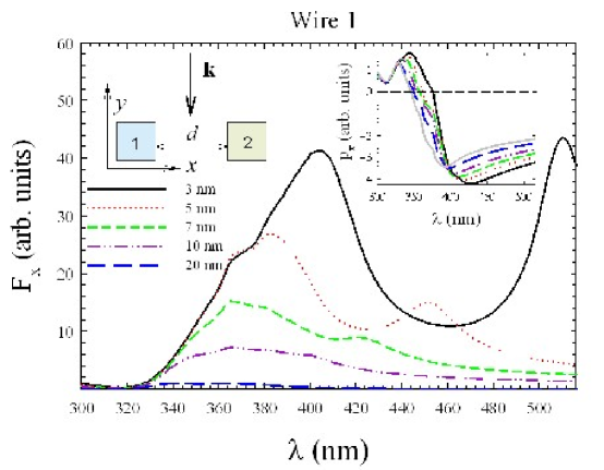
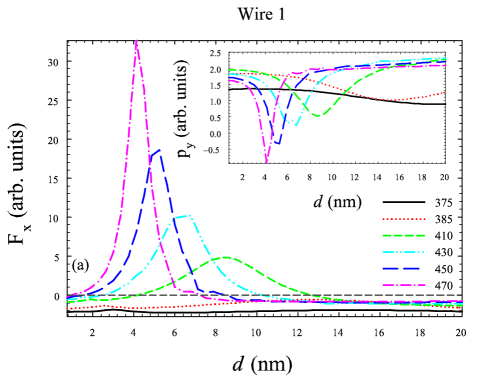
To address this, we begin by examining the forces exerted on the nanowires due directly to the incident wave and the mutual coupling between the wires. The results naturally depend on the propagation direction of the incident field, given by its wavevector . In Fig. 1, we illustrate the -component of the time-averaged force, , on the left wire (wire 1) as a function of the incident field wavelength, , and for various gap distances . The incident electric field vector is polarized along the direction, and the wavevector is directed along . This particular incident field propagation direction yields oppositely directed net forces on each wire that are equal in magnitude. It is evident that is positive for wire 1 over the whole range shown, indicating attraction among the nanowires. It is seen that for much of the range, smaller gaps yield greater maximum values of . All curves show a decrease and blueshift in the peak as increases, except for the nm curve, which shows very little apparent interaction between the wires. This is consistent with a coupled-wire resonance condition that is supported by the inset showing the -component of the dipole moment of wire 1. This quantity is obtained by integrating the appropriate component of the real part of the polarization, , over the cross sectional area of the wire. We show here only since this component of the dipole moment encapsulates the relevant charge distribution involved in interwire coupling. In the inset the solid gray curve shows for reference, for a single isolated wire. Note that the nm curve for is very similar to the solid gray curve, further indicating very little mutual interaction between the wires. For nm, has negative slope and becomes more negative quite rapidly with wavelength. This is approximately the region over which the curves reach their primary peak. It is also interesting that for larger wavelengths, there is another set of peaks that are visible in the , , and nm curves. These peaks become washed out at larger , and approximately correlate with (inset) where the slopes are positive.
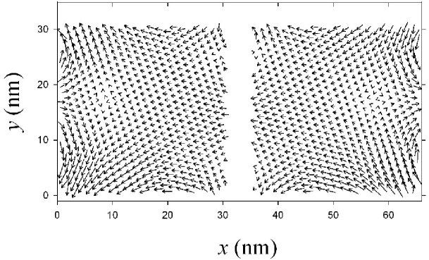
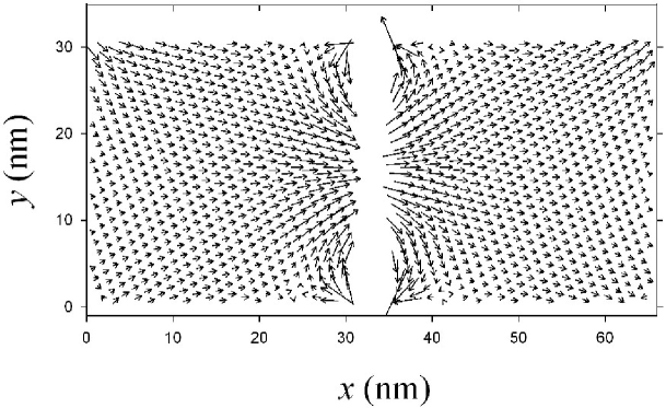
The sign change in the dipole moment exhibited in Fig. 1 is easily visualized by means of vector plots. To this end we show in Fig. 2 the electric field vector distribution within the nanowires. The wires are separated by nm and the top and bottom panels correspond to incident field wavelengths of nm and nm respectively. In the top nm panel, the corner dipole fields are most intense on the outer left and right sides. There is a subsequent nonuniform, strongly position dependent field orientation within the nanowires. The field on the sides nearest the gap region is relatively small compared to the corner fields. In the bottom nm panel, the situation is markedly different. Here the gap field is dominant and different mode patterns arise. These results are consistent with Fig. 1, where at nm is small compared to nm.
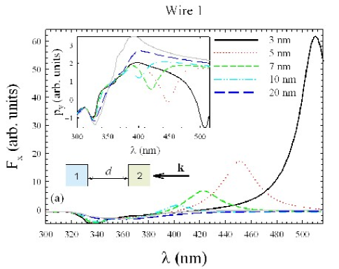
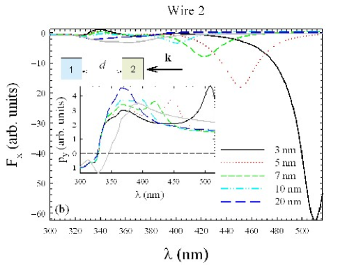
We now vary the incident electric field so that it is now polarized in the direction, and propagates along . We show in Fig. 3, on wire 1 as a function of . Figure 3 depicts the same quantities for wire 2. In general, the net force on each wire is no longer equal in magnitude due to the uneven radiation effects directly from the incident wave. Figure 3 shows that for sufficiently small wire separations ( nm), the force on wire 1 changes sign in a continuous manner as is varied. The force on wire 2 is mainly negative except for a narrow band of in the vicinity of nm (see Figure 3), which correlates to when the force on wire 1 is most negative. Thus the wires experience a repulsion at these wavelengths and separations. For larger separations diminishes and tapers towards zero at higher wavelengths, indicating that electromagnetic coupling between the two wires is negligible. The plasmon resonances within these structures reveal themselves through prominent peaks in the force curves in both figures. The peak positions are strongly dependent on , as they broaden and reduce in magnitude as increases. Comparing the scales in Figs. 1 and 3, we find that the overall resonance effects observed for the forces at small separations is reduced somewhat for this incident field direction. The insets in Fig. 3 show the -component of the electric dipole moment () versus for wires 1 and 2. For wire 1 and nm, Fig. 3 shows that undergoes a minimum at nm and then sharply crosses zero at nm. This trend is similar for the other separations, with only a slight redshifting for larger . For both wire 1 and wire 2 a clear correlation exists between and the associated force; for small enough , the pronounced peaks or depressions in correspond to when is largest. These features therefore become redshifted and spread-out with decreasing separation. As one would expect for nm, the general features of approach that of the limiting case of a single nanowire.
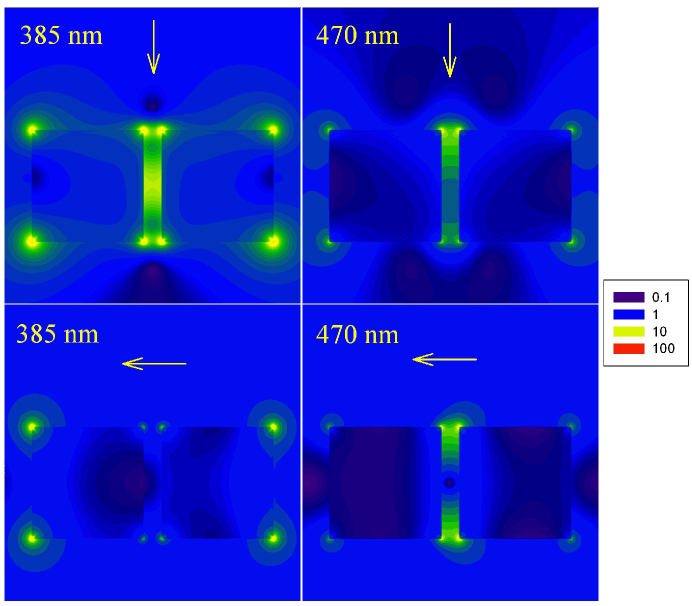
To contrast the near-field electric field patterns for differing incident wave directions, we display in Fig. 4 the electric field amplitudes in the region of the two nanowires. The wires are set at a fixed distance of 5 nm and are illuminated at two different wavelengths. The top two panels correspond to an incident field directed downwards (as shown by the arrows) with nm and nm. The bottom two panels are for an incident electric field traveling towards the left. Beginning with the top left panel, at nm there is a large field enhancement from the corners and within the gap between the wires. This is consistent with Fig. 1, where the force has a maximum at that wavelength. As the wavelength is increased to nm, the system is no longer at resonance and the interaction between the wires has decreased. This follows from Fig. 1, where the force is reduced by nearly a factor of three from its peak value. A different situation is observed in the bottom panels, where at nm the electric field is small between the wires, although the outer corners are still illuminated. At nm, the field amplitude is intensified predominantly within the gap as the nanowires are electrically coupled. There is a clear relationship between the force profiles in Fig. 3 and the field amplitude plots. It is apparent that the incident field “sees” a different geometry based on its orientation relative to the coupled structure; downward propagating waves interact with an effectively larger nanowire in addition to the interwire gap that may support additional modes due to the wire-wire interaction.
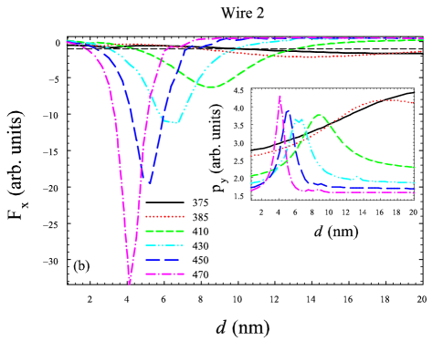
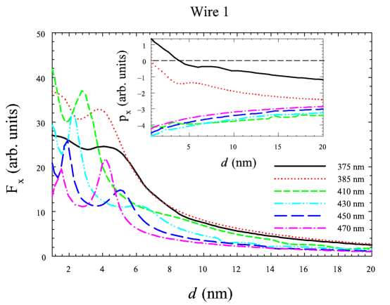
Next, in Fig. 5, the force on each of the two nanowires is shown as a function of the separation distance , and for an incident field directed along . Also shown is the corresponding induced net dipole moment, , for each wire. There are six considered and the variation of with is strongly wavelength dependent. Consider first the longest wavelength, nm where the separation range nm shows a large positive in Fig. 5(a) and a correspondingly large negative in Fig. 5(b). This indicates a resonant condition resulting in a relatively strong attractive force. This is in contrast to the wavelengths, and 385 nm where the curves remain negative and comparatively featureless over the entire range. Clearly no resonant condition occurs for this shorter wavelength as is also evidenced in Fig. 3. These results are consistent with the two lower plots in Fig. 4 that show little gap field enhancement at nm and a large gap field for nm. The inset plots in Fig. 5 are similar in that the maxima in show up as discernible peaks in , reflecting the charge redistribution. In general there is a redshift in the peak values and a sharp decline of as increases, indicating a corresponding shift in the resonance parameters of the mutually interacting wires.
The normalized force, , on the left wire (wire 1) as a function of for an incident field propagating downwards (in the direction) is shown in Figure 6. This figure is analogous to Fig. 5. As in Fig. 1, the force on each wire is equal in magnitude and oppositely directed, yielding an attractive nature over the relatively broad wavelength range studied. The main resonant peaks are present at small separations and then monotonically declines towards zero with increased . The wavelengths that give the largest occur in the range nm. Outside of that range, increasing has the effect of reducing the force and narrowing its peaks. For sufficient separation distances, the force becomes weakly dependent on the wavelength. These characteristics reveal that there are optimal separations and wavelengths to utilize the plasmon driven force enhancement. The inset shows the normalized -component of the dipole moment which is identical in each nanowire. The curves each follow a similar trend, with large separations maintaining a negative dipole moment, while for nm the possibility exists to induce a positive net dipole moment for small separations. Thus for a particular value of it is possible to have a vanishing dipole moment in the wire. This follows from regions within the wire structure that have oppositely oriented polarization vectors that sum to zero.
In conclusion, we have studied the electromagnetic response of two long silver nanowires illuminated by a plane wave with the electric field perpendicular to the axis of the wires. The volume integral approach used here provides accurate solutions to Maxwell’s equations over length scales that are much smaller than the wavelength of the driving field. We found that by varying the wavelength, separation distance, and angle of incidence of the electric field, the collective oscillation of the electrons induced appreciable forces and coupling in the nanowires. The results shown here can play a role in the fabrication and design aspects of optical spectroscopy and waveguiding over nanometer length scales.
Acknowledgements.
This work of K. H. and J.M.E. is funded in part by the Office of Naval Research (ONR) In-House Laboratory Independent Research (ILIR) Program and by a grant of HPC resources from the Arctic Region Supercomputing Center at the University of Alaska Fairbanks as part of the Department of Defense High Performance Computing Modernization Program. S.S. would like to acknowledge support from the ONR/ASEE Summer Faculty Program.References
- (1) R. H. Ritchie, Phys. Rev. 106, 874 (1957).
- (2) J. L. Stanford, J. Opt. Soc. Am. 60, 49 (1970).
- (3) J. P. Kottmann, O. J. F. Martin, D. R. Smith, and S. Schultz, Phys. Rev. B 64 235402 (2001).
- (4) M. Quinten, A. Leitner, J. R. Krenn and F. R. Aussenegg, Opt. Lett. 23 1331 (1998).
- (5) J. C. Weeber, A. Dereux, C. Girard, J. R. Krenn and J. P. Goudonnet, Phys. Rev. B 60 9061 (1999).
- (6) C. Viets and W. Hill, J. Raman Spectroscopy 31 625 (2000).
- (7) R. Elghanian, J. J. Storhoff, R. C. Mucic, R. L. Letsinger and C. A. Mirkin, Science 277 1078 (1997).
- (8) J. P. Kottman and O. J. F. Martin, Opt. Express 8, 655 (2001).
- (9) J. R. Arias-Gonzalez and M. Nieto-Vesperinas, J. Opt. Soc. Am. A 20, 1201 (2003).
- (10) J. J. H. Wang, Generalized Moment Methods in Electrodynamics (Wiley, Toronto, 1991).
- (11) J.D. Jackson, Classical Electrodynamics, 2nd ed. (Wiley, New York, 1975).
- (12) Fletcher, R.,Conjugate Gradient Methods for Indefinite Linear Systems, Lecture Notes in Mathematics 506, (Springer-Verlag Berlin, 1976) pgs. 73-89.
- (13) E. D. Palik, Handbook of Optical Constants of Solids (Academic Press, Washington, D.C., 1985).
- (14) P. Apell and D. R. Penn, Phys. Rev. Lett. 50 1316 (1983).