Anisotropic lattice deformation of InAs self-assembled quantum dots embedded in GaNAs strain compensating layers
Lattice deformations of InAs self-assembled quantum dots, which were grown on (001) GaAs substrates and embedded in GaNAs strain compensating layers (SCLs), were examined with an ion-channeling method in Rutherford backscattering spectrometry. The channeling experiments demonstrated that the increase of the nitrogen concentrations in the GaNAs SCLs caused the indium lattice displacements along the [001] growth direction while those parallel to the (001) crystal plane were kept unchanged It is well-known that InAs self-assembled quantum dots (SAQDs) on (001) GaAs are grown via the lattice mismatch of about 7% between InAs and GaAs. Due to their high crystalline quality of InAs SAQDs, a lot of studies have been performed on their applications to optoelectronic devices[1]–[3]. Especially the applications of SAQDs to optical-fiber communications require SAQDs emission wavelengths at 1.3 m or 1.55 m to fit the minimum optical absorption bands[4]. Although the emission wavelength of 1.3 m has been achieved by a number of groups[5], the wavelength of 1.55 m has been difficult due to the compressive strain induced within InAs SAQDs during the embedding processes with GaAs[6]. This strain issue has been coped with apparently opposite methods. One is to embed InAs SAQDs with InGaAs strain reducing layers (SRLs)[7]-[8], which reduce the interface lattice mismatch between InAs SAQDs and InGaAs SRLs by increasing indium (In) in the SRLs. However the higher In concentrations in the SRLs will accumulate the amount of overall compressive strain in the system, which may degrade the photoluminescence (PL) efficiencies by the possible generations of nonradiative recombination centers due to the excess strain. The other method is to embed InAs SAQDs in tensile-strained GaNAs strain compensating layers (SCLs)[9]. This method may increase the mismatch at the InAs/GaNAs interfaces, but the overall average strain in the system can be minimized by compensating the compressive strain in the InAs SAQDs with the tensile strain in the GaNAs SCLs. Sasikala et al. realized 1.55 m emission from InAs SAQDs embedded in GaNAs SCLs with the nitrogen (N) concentration of 2.7%[10]. Although GaNAs usually shows degraded PL efficiencies with the increase of the N concentrations, the luminescence from the InAs SAQDs embedded in the GaNAs SCLs showed the improved efficiencies up to 5-times with the increase of the N concentrations[10]–[11]. However, the details of the strain distribution within and around the InAs SAQDs are not well understood.
In this letter, the lattice deformations of InAs SAQDs embedded in GaNAs SCLs were examined with ion channeling in Rutherford backscattering spectrometry (RBS). The channeling investigations are highly sensitive to atomic displacements[12]–[13]. Clear dependences of the anisotropic In lattice displacements on the N concentrations in the GaNAs SCLs will be demonstrated, and the strain relation between the InAs SAQDs and the GaNAs SCLs will be discussed.
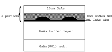
All the InAs SAQDs samples were grown on (001) GaAs substrates by metalorganic molecular-beam epitaxy (MOMBE). The metalorganic precursors used in this study were triethylgalium(TEGa), triethylindium(TEIn) , trisdimethylaminoarsenic(TDMAAs), and monomethylhydrazine(MMHy) for Ga, In, As, and N, respecitvely. A 300-nm-thick GaAs buffer layer was firstly grown at the substrate temperature of . Subsequently the substrate temperature was lowered to and about 2.0 MLs of InAs were grown. A transition from the two-dimensional to three-dimensional growth mode, i.e., the initiation of the Stranski-Krastanow growth mode of the InAs layer was monitored with reflection high- energy electron diffraction by the diffraction pattern change from streaky to spotty ones. A 10-nm-thick GaNAs SCL and a 10-nm-thick GaAs layer were subsequently grown at the same substrate temperature of . Following this sequence, three stacks of the InAs SAQDs layers were grown. Three samples with the N concentrations of 0.7, 1.4, and 2.65% in the GaNAs SCLs were prepared. The schematic of the sample structure is shown in Fig. 1.
A standard experimental arrangement for ion channeling was used with a tandem-type ion accelerator at Kanagawa High-Technology Foundations. The samples were set on a three- axis goniometer. 2.34 MeV ions were used as a probe beam to investigate both [001] and channeling properties. The scattering angle and the beam spot were and 1mm, respectively. To evaluate the lattice deformation, the normalized minimum backscattering yield, , which is defined as the ratio of aligned yields to random ones, was used. Since the relative displacement of In atoms from the GaAs host lattice increases the scattering of the incident ions, the increase of the minimum backscattering yield, , sensitively reflects the lattice distortion due to the strain.
One of the RBS spectra measured under the random, [001] and channeling geometries are shown in Fig. 2. The InAs SAQDs sample shown in Fig. 2 was embedded in the GaNAs SCL with the N concentration of 0.7%. The inset shows In signals detected around the channel number of 430. The filled circles, triangles, and squares indicate the random spectrum, the [001] and spectra, respectively. Due to the channeling effect, drastic decreases of the backscattering yield in the [001] and channeling geometries were clearly observed compared with that in the random one. Usually the channeling in the directions is more enhanced and the backscattering yields in this direction are lower than those in the directions. However the present RBS measurements on the InAs SAQDs embedded in the GaNAs SCLs resulted in the reversed trend, i.e., higher backscattering yields in the channeling direction than those in the [001] direction. This peculiar trend was observed in all the samples measured in this study and this point will be discussed later.
The N concentration dependence of the minimum backscattering yield for In is summarized in Fig. 3. This result reveals a significant difference between [001] and . Although [001] did not change significantly regardless of the N concentration in the GaNAs SCL, showed the drastic increase with the increase of the N concentration in the SCL. Since the backscattering in the channeling direction reflects the In lattice tetragonal deformations, this [001] and dependences demonstrate that the vertical distortion of the In lattices in the InAs SAQDs dominates with the increase of the N concentration in the GaNAs SCLs, while keeping their In lattices in the (001) plane nearly unchanged.
In addition to the examination of the In lattices in the InAs SAQDs, the channeling properties of the Ga and As lattices around the channel number of 400 were studied, where the 10-nm-thick GaNAs SCLs/10-nm-thick GaAs layers burying the InAs SAQDs close to the sample surface mainly contribute. Figure 4 summarizes the N concentration dependence of the measured . Although [001] for the Ga and As lattices remained almost unchanged, showed the clear increase for the higher N concentrations in the GaNAs SCLs. This N concentration dependence is very similar to that observed for In atoms. The RBS measurements shown in Figs. 3 and 4 demonstrate that the deformations of both the In lattices in the InAs SAQDs and the Ga and As lattices in the GaNAs SCLs are mainly in the vertical direction to the (001) plane.
In the present RBS measurements, the reversal of the minimum scattering yields in the [001] and channeling directions was observed compared with unstrained bulk crystal measurements as discussed above on Fig. 2. This reversed trends will be attributed to the strain-induced lattice distortions. The tetragonal lattice distortions suggested by the results shown in Figs. 3 and 4 will more critically influence the channeling direction, which is inclined relative to the (001) surface, compared with the [001] direction normal to the (001) surface. This will make the observed reversal of the values relative to the unstrained lattices probable.
We have previously shown that measured in channeling directions are dependent on the sizes of InAs SAQDs buried near the sample surfaces, i.e., measured from samples with larger-sized dots is larger than those measured from samples with smaller- sized dots[14]. In this regard, the InAs SAQDs in the present study were prepared under the same conditions for all the samples. Although there remains the possibility that the sizes and shapes of InAs SAQDs may change during the embedding processes, the observation of the nearly constant in the [001] direction in this study will exclude such deformation of InAs SAQDs during the embedding processes with the GaNAs SCLs.
The concept of the InGaAs SRLs[7]–[8] is based on the reduced interface mismatch between InAs/(In)GaAs heterointerfaces. The formation of the InAs/GaNAs heterointerfaces in this regard will apparently increase the interface lattice mismatch. The present observations showed that the In lattices in the (001) crystal planes of the InAs SAQDs were not much affected through the embedding processes with the GaNAs SCLs. On open InAs SAQD surfaces, however, surface In atoms experience the stress-free condition and the lattice extensions in both surface normal and lateral directions will take place. Formation of As-Ga bonds on this surface will induce compressive strain in the surface In-As bonds and tensile strain in the adsorbed As-Ga bonds. S. B. Zhang et al discussed the surface-reconstruction-enhanced solubility of N in III-V semiconductors based on a calculation of the substitutional energy of N atoms in binary (001) films[15]. The main mechanism to enhance the N solubility beyond the thermal equilibrium limit in III-V was discussed to be the reduction of the compressive strain underneath the surface anion dimers by the N incorporation in the sub-surface lattice sites. The present situation will be very similar in the sense that the N incorporation in the As sites in the compressively strained surface In-As bonds will reduce the compressive strain underneath the surface-formed As-Ga bonds. This mechanism may help to keep the overall coherent growth condition which keeps the (001) lattice structure unchanged.
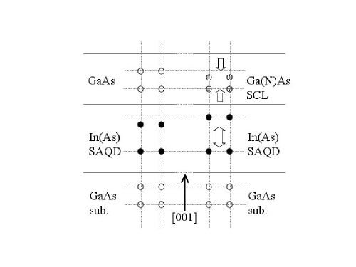
The deformations of the In lattices in the InAs SAQDs and the Ga and As lattices in the GaNAs SCLs in the direction normal to the (001) crystal plane and their deformation enhancements with the increase of the N concentrations in the GaNAs SCLs observed in this work will be schematically represented as shown in Fig. 5. The InAs lattice will experience bi-axial compression and will extend toward the direction normal to the (001) surface. However embedding them with GaAs layer will induce the additional compressive strain normal to the (001) surface. The partial replacement of the GaAs embedding layer with the tensile-strained GaNAs layers will shrink themselves normal to the (001) surface and this allows the InAs lattice to recover the expansion normal to the (001) surface as shown in Fig. 5. This strain release in the InAs SAQDs will explain the observed red-shift up to 1.55m with the GaNAs SCLs reported in Ref.10.
In summary, the lattice deformation of InAs SAQDs was examined with the RBS ion- channeling method. InAs SAQDs embedded in GaNAs SCLs showed the significant increase of the back scattering yields in the channeling direction with the increase of the N concentrations in the GaNAs SCLs, while the backscattering yields in the [001] channeling direction remained nearly the same. These results demonstrated that the lattice distortions caused by the embedding processes of InAs SAQDs with the GaNAs SCLs are dominated in the direction normal to the (001) surfaces.
References
- [1] Y. Arakawa and H. Sasaki, Appl. Phys. Lett. 40, 939 (1982).
- [2] M. Tabuchi, S. Noda and A. Sasaki, Sci. & Tech. Mesoscopic Structures, 379 (1992).
- [3] D. Leonard, M. Krishnamurthy, C. M. Reaves, S. P. Denbaars and P. M. Petroff, Appl. Phys. Lett. 63, 3203(1993).
- [4] N.-T. Yeh, T.-E. Nee J.-I. Chyi, T. M. Hsu and C. C. Huang, Appl. Phys. Lett., 76, 1567(2000).
- [5] For example, K. Mukai and M. Sugawara, Appl. Phys. Lett. 74, 3963(1999).
- [6] H. Saito, K. Nishi and S. Sugou, Appl. Phys. Lett. 73, 2742(1998).
- [7] K. Nishi, H. Saito, and S. Sugou, J.-S. Lee, Appl. Phys. Lett. 74, 1111 (1999).
- [8] J. Tatebayashi, M. Nishioka and Y. Arakawa, Appl. Phys. Lett. 78, 3469(2001).
- [9] X. Q. Zhang, S. Ganapathy, H. Kumano, K. Uesugi and I. Suemune, J. Appl. Phys., 92, 6813(2002).
- [10] S. Ganapathy, X. Q. Zhang, H. Kumano, K. Uesugi and I. Suemune, Jpn. J. Appl. Phys., 42, 5598(2003).
- [11] X. Q. Zhang, S. Ganapathy, I. Suemune, H. Kumano, K. Uesugi, Y. Nabetani, and T. Matsumoto, Appl. Phys. Lett. 83, 4524 (2003).
- [12] T. Haga, T. Kimura, Y. Abe, T. Fukui and H. Saito, Appl. Phys. Lett., 47, 1162(1985).
- [13] L. C. Feldman, J. W. Mayer, and S. T. Picraux: Material Analysis by Ion Channeling (Academic, New York, 1982).
- [14] N. Matsumura, T. Haga, S. Muto, Y. Nakata, and N. Yokoyama, J. Appl. Phys. 89,160(2001).
- [15] S. B. Zhang, and A. Zunger, Appl. Phys. Lett. 71, 677(1997).
Figure captions
-
Figure 1
Schematic of InAs SAQDs sample embedded in GaNAs SCL.
-
Figure 2
Typical RBS/channeling spectra for InAs SAQDs embedded in GaNAs SCL. Inset shows In signals near 430 ch.
-
Figure 3
Normalized minimum backscattering yield () of In atoms as a function of the N concentration in the GaNAs SCL.
-
Figure 4
Normalized minimum backscattering yield () of Ga and As stoms in GaNAs SCL as a function of the N concentration in the GaNAs SCL.
-
Figure 5
Schematic of lattice distortion of InAs SAQDs embedded in GaAs (left) and in GaNAs (right).