Giant Low-temperature Piezoresistance Effect in AlAs Two-dimensional Electrons
Abstract
We present piezoresistance measurements in modulation doped AlAs quantum wells where the two-dimensional electron system occupies two conduction band valleys with elliptical Fermi contours. Our data demonstrate that, at low temperatures, the strain gauge factor (the fractional change in resistance divided by the sample’s fractional length change) in this system exceeds 10,000. Moreover, in the presence of a moderate magnetic field perpendicular to the plane of the two-dimensional system, gauge factors up to 56,000 can be achieved. The piezoresistance data can be explained qualitatively by a simple model that takes into account intervalley charge transfer.
The piezoresistance effect Bridgman (1932) – the change of a device’s electrical resistance as a function of applied stress – is of great technological interest. It is used to make force, displacement, and pressure sensors Belu-Marian et al. (1992) that are ubiquitous in various industries. Even the semiconductor industry is using the piezoresistance effect to improve the performance of field-effect transistors Keyes (2002). Recently, piezoresistivity has found use in measuring sub-nanometer (0.01nm) displacements of tips in atomic force microscopes Tortonese et al. (1993); Harley (2000). With the advancements in science and technology of materials and devices whose size approaches the atomic scale, the interest in sensors that can detect ultra-small forces and distances is likely to grow even higher. Piezoresistance is also useful as a probe of the electronic properties of materials.
There are two main sources of the piezoresistance of a strain gauge. First, applied stress changes the resistance of the gauge by altering the length and the cross sectional area of the gauge. This geometrical distortion is the primary source of piezoresistance in metallic films. The sensor’s gauge factor, defined as the fractional change in the film’s resistance divided by the fractional change in its length, is determined primarily by the solid’s Poisson ratio, and is typically about 2. Second, stress can modify the electronic structure of a solid and lead to large changes in its resistivity. This change can be particularly significant in indirect band gap semiconductors such as Si and Ge (and AlAs), where the conduction electrons occupy multiple minima (valleys) in the conduction band. In this case, uniaxial or shear stress breaks the symmetry of the band structure, lifts the degeneracy of the valley energies, and causes an intervalley charge transfer. Since the valleys often have anisotropic effective masses, such a transfer leads to significant changes in electron mobility, and therefore resistance, along certain crystallographic directions of the solid. This phenomenon is well-known for bulk Si and Ge Smith (1954); Herring (1955) as well as for two-dimensional electron systems (2DESs) in Si-MOSFETs Eisele (1978) where gauge factors as large as have been observed. Here we report a giant low-temperature piezoresistance effect, characterized by gauge factors exceeding 10,000, for 2DESs confined to modulation-doped AlAs quantum wells. Moreover, we show that even much larger gauge factors can be achieved if the sample is placed in a moderate, perpendicular magnetic field.
AlAs is an indirect gap semiconductor with conduction-band valleys at the Brillouin zone X-points. Its constant energy surface consists of three highly anisotropic ellipsoids (six half-ellipsoids) with longitudinal ( and transverse () effective masses and (in units of free electron mass), respectively. We designate these valleys by the direction of their major axes, which point along the 100 directions. In AlAs quantum wells wider than nm grown on GaAs (001) substrates, because of the GaAs-AlAs lattice mismatch strain, only the two valleys with their major axes lying in the plane of the 2DES are occupied Maezawa et al. (1992). While in the absence of an external stress these valleys are energy degenerate, a compression along either 100 or 010 breaks this degeneracy and causes a redistribution of electrons between the valleys. Although the band structure of Si and AlAs are similar, the valleys in Si are centered around the six -line points that are away from the Brillouin zone edge. As a result, there are six valleys in Si, two valleys along each of the 100 directions. An additional difference is that, in the absence of applied stress, in (001) Si-MOSFETs two out-of-plane valleys are occupied, while in a wide (001) AlAs quantum well the 2D electrons occupy two in-plane valleys.
Our samples contain 2D electrons confined to an 11 nm-wide, AlAs quantum well grown on a GaAs (001) substrate by molecular beam epitaxy De Poortere et al. (2002). The quantum well is flanked by Al0.4Ga0.6As barrier layers and is modulation doped with Si. Using a metal electrode (gate) deposited on the top surface, we can vary the 2DES density , between and m-2. To assure a uniform strain in the 2D layer, the substrate thickness is kept below 250 m. The resistance is measured using a lock-in amplifier at 0.3 K on an etched Hall bar mesa aligned with the [100] crystal direction. Piezoresistance measurements were performed on three samples. Here we concentrate on the data from one sample, with other samples corroborating the results.
We strain the sample by gluing it to a commercial piezoelectric stack (piezo) with the [100] crystal direction aligned to the poling direction of the piezo Shayegan et al. (2003). To shield the 2DES from the electric fields in the stack, we evaporated a 120 nm thick Ti/Au gate on the back of the sample’s substrate and kept it under constant bias throughout the measurements. Under a positive bias applied to the piezo, its surface expands along the poling direction and shrinks in the perpendicular direction. This deformation is transmitted to the sample through the glue. Using a calibrated, metal strain gauge glued to the piezo’s opposite side, we monitor the applied strain with a relative accuracy of 5%. Via this technique, we can vary the shear strain (difference in the fractional change of length along the [100] and [010] directions) by . Since the negative of the ratio of the lateral to the longitudinal deformation of the piezo is 0.38 Shayegan et al. (2003), close to the Poisson ratio of AlAs (), the resulting sample stress is almost uniaxial; tensile stresses along [100] and [010] are equal to 73 and 8.3 (in GPa), respectively. All other stress tensor components are zero.
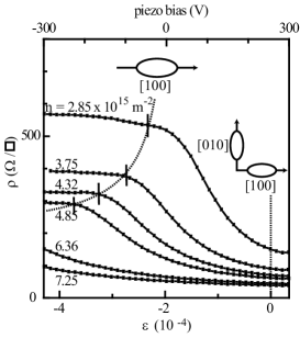
We show the results of our longitudinal piezoresistance measurements in Fig. 1. Each trace corresponds to the resistivity along [100] at a constant 2DES density, with the piezo bias swept from -300V to 300V. As the sample is compressed along the [100] direction, the resistivity of the sample first increases with increasing magnitude of strain, and then saturates. This behavior of the resistivity is consistent with the transfer of electrons out of the [010] valley (with smaller effective mass along [100]) and into the [100] valley (with larger effective mass along [100]). The transfer of charges is corroborated by the change of the frequency composition of the Shubnikov de Haas oscillations. Using these oscillations, we determine and mark two strains for each trace; right dotted line indicates the (zero) strain at which both valleys are equally occupied, while the left dotted line indicates the strain at which the [010] valley depopulates.
Since the resistivity in our sample is a nonlinear function of strain, to quantify the piezoresistance we concentrate on the differential gauge factor . The maximum value varies between 11,700 and 6,200 for the density range m-2. A quantitative fit of the entire piezoresistivity curve requires a detailed knowledge of both intervalley and intravalley scattering mechanisms Keyes (1960). However, we can understand the major features of this curve using a simple model in which we assume that the electron scattering lifetimes in the two valleys are equal, isotropic, and independent of the electron concentration in either valley, and ignore intervalley scattering. We also use eV for the electron shear deformation potential of AlAs Charbonneau et al. (1991). This model predicts that for a strain of , which transfers all the electrons into a single valley, the resistance increase should be . For m-2, the predicted strain, , and the factor of increase in resistance are consistent with the experimentally observed values.
Our maximum strain gauge factor (=11,700 for m-2 is about 8 times larger than previously reported in (001) Si-MOSFETs Eisele (1978), although the deformation potential of Si (8.2 eV) and AlAs are close as are the electron effective masses. A factor of two of this increase can be attributed to the higher density ( m-2) of the Si samples that were studied Eisele (1978) and to the band structure differences between Si and AlAs. We do not know what causes the remaining difference, but speculate that it is the result of the non-monotonic strain dependence of the resistance caused by the strong intervalley scattering in Si samples Dorda et al. (1978).
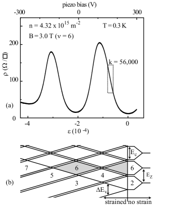
In the presence of a moderate magnetic field perpendicular to the AlAs 2DES plane, the piezoresistivity increases dramatically, with observed strain gauge factors as large as 56,000 [see Fig. 2(a)]. This giant piezoresistance effect results from the change of the 2DES density of states (DOS) in . With a finite , the orbital motion of electrons becomes quantized; the DOS [shown in Fig. 2(b)] is no longer a constant function of energy, and instead has non-zero values only at energies of the Landau levels. If the magnitude of is such that an integer number of Landau levels are filled (integer filling factor ), the system’s Fermi energy falls in an energy gap (DOS gap). This gap inhibits electron scattering at low temperatures, leading to a smaller 2DES resistivity. With applied stress, the Landau levels corresponding to different valleys cross, causing the gap to close and the 2DES resistivity to increase. Since the resistivity depends exponentially on the size of the energy gap, its change can be much larger than the effective mass anisotropy. The gap at vanishes when is equal to the cyclotron energy () of the system. Since (for a large range of ), the Landau level crossings occur at strains smaller than required to depopulate the [010] valley. The greater change in resistivity over a smaller strain change results in strain gauge factors that are much larger than those possible at zero .
Nonlinearity of the piezoresistive response outside a narrow range of strain limits the usefulness of the in-field strain gauge to applications in which only small deformation is present. One can extend the measurable strain range by employing a technique inspired by Michelson interferometry. As seen in Fig. 2(a), the resistance oscillates periodically with strain in a fixed magnetic field (see also Shayegan et al. (2003)). These periodic oscillations, which are easy to detect thanks to the large () ratio of maximum to minimum , allow one to accurately measure very large strains just by counting the number of oscillations.
We have shown that a combination of confinement and magnetic field leads to a giant piezoresistive response in AlAs 2DESs at low temperatures. This effect may find important applications. Indeed, the gauge factor of 56,000 is large enough to detect nanometer elongations of a centimeter-long sample by a simple multimeter. With improved sample quality, the gauge factor can be further increased at both zero and high magnetic fields. At , one can achieve a higher gauge factor by further lowering the density of the 2DES. At high , the 2DES can undergo a strain-induced transition from a quantum Hall state (with nearly zero resistance) to a very high resistance neighboring (insulating) state, with a very high resistance, leading to an even larger piezoresistance effect. One-dimensional confinement, such as in a ballistic quantum point contact van Houten et al. (1988), could also result in large gauge factors; the resistance of the point contact can be extremely sensitive to the number of occupied one-dimensional channels and therefore the valley occupancy.
We thank the ARO, NSF, and the Humboldt Foundation for support, and K. Karrai for illuminating discussions.
References
- Bridgman (1932) P. W. Bridgman, Phys. Rev. 42, 858 (1932).
- Belu-Marian et al. (1992) A. Belu-Marian, E. Candet, and A. Devenyi, Thin film resistive sensors (IOP Publishing, 1992), p. 113.
- Keyes (2002) R. W. Keyes, IEEE Circuits Devices Mag. 18, 36 (2002).
- Tortonese et al. (1993) M. Tortonese, R. Barrett, and C. Quate, Appl. Phys. Lett. 62, 1993 (1993).
- Harley (2000) J. A. Harley, Ph.D. thesis, Stanford University (2000).
- Smith (1954) C. S. Smith, Phys. Rev. 94, 42 (1954).
- Herring (1955) C. Herring, Bell Syst. Tech. J. 34, 237 (1955).
- Eisele (1978) I. Eisele, Surf. Sci. 73, 315 (1978).
- Maezawa et al. (1992) K. Maezawa, T. Mizutani, and S. Yamada, J. Appl. Phys. 71, 296 (1992).
- De Poortere et al. (2002) E. P. De Poortere, Y. P. Shkolnikov, E. Tutuc, S. J. Papadakis, M. Shayegan, E. Palm, and T. Murphy, Appl. Phys. Lett. 80, 1583 (2002).
- Shayegan et al. (2003) M. Shayegan, K. Karrai, Y. P. Shkolnikov, K. Vakili, E. P. De Poortere, and S. Manus, Appl. Phys. Lett. 83, 5235 (2003).
- Keyes (1960) R. W. Keyes, Solid State Phys. 11, 149 (1960).
- Charbonneau et al. (1991) S. Charbonneau, J. F. Young, P. T. Coleridge, and B. Kettles, Phys. Rev. B 44, 8312 (1991).
- Dorda et al. (1978) G. Dorda, I. Eisele, and H. Gesch, Phys. Rev. B 17, 1785 (1978).
- van Houten et al. (1988) H. van Houten, C. W. J. Beenakker, P. H. M. van Loosdrecht, T. J. Thornton, H. Ahmed, M. Pepper, C. T. Foxon, and J. J. Harris, Phys. Rev. B 37, 8534 (1988).