Green’s Function Technique for Studying Electron Flow in 2D Mesoscopic Samples
Abstract
In a recent series of scanning probe experiments, it became possible to visualize local electron flow in a two-dimensional electron gas. In this paper, a Green’s function technique is presented that enables efficient calculation of the quantity measured in such experiments. Efficient means that the computational effort scales like ( is the width of the tight-binding lattice used, and is its length), which is a factor better than the standard recursive technique for the same problem. Moreover, within our numerical framework it is also possible to calculate (with the same computational effort ) the local density of states, the electron density, and the current distribution in the sample, which are not accessible with the standard recursive method. Furthermore, an imaging method is discussed where the scanning tip can be used to measure the local chemical potential. The numerical technique is used to study electron flow through a quantum point contact. All features seen in experiments on this system are reproduced and a new interference effect is observed resulting from the crossing of coherent beams of electron flow.
I Introduction
Electronic transport properties in mesoscopic systems have gained a lot of attention in the last two decades (for a review see e.g. Refs. Datta, ; Ferry, ). A lot of effort already went into the study of global transport quantities (mainly conductance), and a range of interesting phenomena emerged: e.g. quantized conductance in a point contact vanWees , quantum Hall effect vonKlitzing , and universal conductance fluctuations Lee to name a few.
Recently, scanning probe methods have offered the interesting possibility of obtaining local information on electron transport, not accessible with ordinary global measurements. For example, by using the tip of an STM as a localized scatterer of electrons and measuring the conductance change of the sample as a function of tip position, it has been possible to obtain a spatial map of electron flow in a two-dimensional electron gas TopinkaScience ; TopinkaNature ; TopReview . Such visualizations of current flow are interesting both from an experimental and a theoretical point of view.
The results obtained in these experiments were mainly interpreted with the help of electron or flux density calculations. Here, a numerical technique is developed that allows to calculate in an efficient way the quantity that is actually measured, which is a conductance difference as a function of the tip position. The standard recursive Green’s function method used in Ref. HeZhuWang, to obtain the same result is not very efficient because one has to start over the complete conductance calculation for every position of the tip. The numerical effort then scales like in the number of operations, where is the width and is the length of the system (), and one therefore is limited to small systems. On the other hand, our method scales like for the same problem. Moreover, with our method it is straightforward to obtain other relevant information like the local density of states and the electron and current density distributions which can then be compared with the experimental observables. All these quantities can be calculated with the same computational effort scaling like , whereas they are unavailable with the standard technique.
The imaging technique with the tip as a scatterer will not always give the expected results in the regime of high magnetic fields. To obtain more information about electron flow in this high field range, a measuring method is proposed where the STM tip is used as a local voltage probe. This method can also be treated within the proposed numerical framework, with a computational effort scaling again as .
The paper is subdivided as follows. In the next section, the imaging method used in Refs. TopinkaScience, ; TopinkaNature, is briefly reviewed and the voltage probe method is described. In section III, we discuss how the considered systems can be described within a tight-binding model. Subsequently, the numerical method is presented in some detail in section IV and in the appendices. Finally, the method is applied to study electron flow through a quantum point contact.
II Imaging Methods
II.1 Tip as a Local Scatterer
The experiments in Refs. TopinkaScience, ; TopinkaNature, take place as follows: current is passed via two Ohmic contacts through a two-dimensional electron gas, while simultaneously a scanning probe tip is moved across the sample. The local electrostatic potential that results from a negative voltage on the tip can function as a scattering center for electrons in the device. If the tip is placed over a region where a lot of electrons are flowing, the conductance of the sample will decrease considerably because of enhanced backscattering due to the tip, whereas in an area of low electron flow, the conductance decrease will be small. As such, by mapping the conductance decrease of the sample to the tip position, one gets a spatial profile of electron flow.
The relevant quantity for this imaging method is thus the position dependent conductance difference:
| (1) |
where is the conductance with the tip positioned on a point and is the conductance without the tip. Conductances can be calculated within the Landauer-Büttiker formalism, which relates conductance to the electron transmission coefficient between the contacts on opposite sides of the sample:
| (2) |
Please note that since is a two-terminal conductance, it is symmetric with respect to reversal of the direction of an applied magnetic field: Buettiker , and therefore the map of electron flow obtained with this scattering method has the same symmetry.
II.2 Tip as a Voltage Probe
The imaging method in the previous section can give very nice visualizations of the electron flow, as proven by the experimental results of electron transport through a quantum point contact TopinkaScience ; TopinkaNature . One of the interesting subjects to study with this imaging method would be the quantum Hall effect, because even after intensive theoretical and experimental effort since its discovery vonKlitzing , some of the details of electron transport in this regime remain unclear. Unfortunately, the appearance of edge states in the high field regime leads to the suppression of backscattering Butt , so that the method described above will not yield the expected results in the quantum Hall limit.
However, a picture of this edge-state transport can be obtained by investigating the local chemical potential in the sample. This can be done using the STM tip as a voltage probe; the STM tip voltage equilibrates itself to the local chemical potential when electrons are allowed to tunnel into and out of the tip. Experimentally, this technique has already been used to probe the potential distribution at metal-insulator-metal interfaces Muralt and at grain boundaries Kirtley . Gramespacher et al. have studied this measurement mode theoretically, and found Green’s function expressions for the sample-tip transmission coefficients which generalize the Bardeen formulas Gramespacher1 . For weak coupling between the probe and the sample, these transmission coefficients can be expressed in terms of so-called partial densities of states Gramespacher2 .
In the following, we will however start again from the standard Landauer-Büttiker formalism, but now one has three contacts: the left and right contact through which a fixed current is passed, and the STM tip that measures a voltage. For this 3-lead structure at temperature , one obtains the following expression for the voltage measured on the tip Datta :
| (3) |
with the voltage on lead . Our numerical method thus should be able to calculate the transmission coefficients from the left and right contact to the STM tip, as a function of the position of the tip.
It should be indicated that this imaging mode corresponds to making a three-terminal measurement. This means that the spatial map one obtains will not be invariant under the reversal of the direction of an applied magnetic field. The only symmetry relations that hold are: Buettiker . Therefore, it should be clear that the information obtained when the tip is used as a voltage probe is different from that when the tip is used as a local scatterer, and as such both imaging methods will contribute differently to our understanding of electron flow in 2D systems.
II.3 Charge and Current Density
One can (at least in principal) experimentally observe the total current density in the sample, by measuring the magnetic field it induces. Another physically observable quantity is the total charge density, due to the electrostatic field it generates. Both of these quantities can also be calculated within the numerical framework presented in the next sections.
Since we have access to the electron density, it would also be possible to include self-consistently the effect of the applied voltage and the resultant current flow on the transport properties. However, this will not be pursued further in the current paper.
III System Modelling
The system we will consider is a two-dimensional device connected to two semi-infinite leads extending in the x-direction. By discretizing the Schrödinger equation, one obtains the standard nearest neighbor tight-binding model for the system Hamiltonian:
| (4) |
where label the sites on the lattice, and are the on-site energies. Note that the sites are not meant to represent atoms as in the usual tight-binding model; rather they may represent a region containing many atoms, but this region should be small with respect to physically relevant quantities such as the Fermi wavelength. The quantities and in Eq. (4) give the hopping amplitude in the horizontal, respectively vertical direction. A square lattice is assumed, so in the absence of a magnetic field one has:
| (5) |
with the lattice spacing, and the effective mass of the electron.
The leads extend from for the left lead, and for the right one. The device itself is comprised by the other sites. In the leads, only homogeneous fields perpendicular to the 2D device will be considered, while both homogeneous and inhomogeneous fields can be treated in the central device. The fields are described by Peierls substitution Peierls , which changes the hopping parameters as:
| (6) |
where is the integral of the vector potential along the hopping path.
IV Numerical Method
IV.1 Introduction
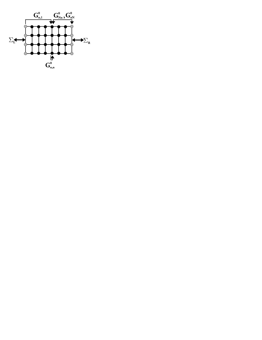
In sections II.1 and II.2, it was shown that the basic quantities that need to be calculated in order to describe the scanning probe experiments are transmission coefficients from one lead to another. In the next sections, it will be shown that these transmission coefficients, and as a matter of fact all other quantities we wish to calculate (density of states, current density distribution,…) can be expressed in terms of the Green’s function matrices , , and (for all possible values of ). These matrices are defined as:
| (7) |
where
| (8) |
is the Green’s function of the device without the influence of the tip. In this expression, is the Hamiltonian of the central device disconnected from the leads, while and are self-energies of the left respectively right lead. The Green’s functions are thus submatrices of connecting points from column to those of column of the lattice (see also Fig. 1).
The method that is used to calculate these Green’s functions will be presented in Appendix A, the main result being that they can be obtained with a number of operations that scales like . As for the self-energies of the leads, they can be calculated in several ways: in the absence of a magnetic field they are known analytically Datta , while in the case of a homogeneous magnetic field one needs to resort to numerical methods, for instance based on the solution of the so-called Harper’s equation Guan . However, we have chosen for another method, originally developed for the calculation of surface electronic structure, that is described in full detail in Refs. LopezSancho, ; Turek, .
IV.2 Local Scatterer Method
In our calculations, the scattering potential created by the STM tip is modelled by a delta function located on a site , so it adds a repulsive contribution to the on-site energies in the Hamiltonian (4). Like explained in section II.1, one has to calculate a conductance difference:
| (9) |
for every tip position in order to obtain the spatial map of electron flow in the sample. The transmittance between the left and right lead can be calculated by Datta :
| (10) |
with related to the retarded self-energies of the left (right) lead as:
| (11) |
and is the Green’s function between columns and . The matrix includes the effect of the STM tip, and is therefore different from , mentioned in the introduction.
In Ref. HeZhuWang, , one uses the standard recursive Green’s function method for calculating : first, the system is divided into its separate columns (by making the hopping matrices between them zero), and the repulsive potential is added on a certain site. Subsequently the columns are attached one by one making use of Dyson’s equation. For this attachment procedure, inversions of an matrix are needed to obtain for a single tip position. Since this procedure has to be started over and over again for every single position of the tip, the total number of inversions needed to calculate for all positions scales as (in the limit of large N), which translates into a total computational effort scaling like (computational effort to invert an matrix scales as ).
However, supposed that we have access to the Green’s functions , and (see Appendix A), we are able to do things more efficient, by including the effect of the tip with Dyson’s equation:
| (12) |
where is the potential introduced by the tip, . Projecting (12) between columns and , one obtains (it is assumed that the tip is located at lattice site ):
| (13) |
Since has only one non-zero element, the inversion will boil down to the inversion of a scalar. This means that no extra matrix inversions are needed to find for an arbitrary lattice position of the tip, once we have the , and for all ! In Appendix A, we will show a way of calculating these functions with a number of matrix inversions that scales linear with , so that the computational effort for calculating for all tip locations scales as .
At first sight, it might seem that this efficiency is decreased for the complete calculation because one has to evaluate the trace in Eq. (10) for every tip position, which involves products of matrices. The computational effort for doing such a product scales like , and since there are lattice sites, the total effort would scale as . However, we have a better way of evaluating this trace, scaling as , so that we do not loose our efficiency. Technical details will be described in Appendix B.
It now is clear that our method, scaling like , is more efficient than the standard recursive technique, which scales like for the same problem.
IV.3 Voltage Probe Method
In this case, the STM tip will be modelled by a one-dimensional semi-infinite lead, attached to the central device at position (the lead can be thought to extend in a direction perpendicular to the 2D sample). The voltage on the tip can be written as a function of the transmission coefficients and between the STM tip and the left and right leads (Eq. (3)). These transmittances, with the tip positioned over site , can be expressed as:
| (14a) | |||||
| (14b) | |||||
where . Since the lead modelling the tip is one-dimensional, one does not have to take care of magnetic field effects in this lead, and the self-energy of the tip is known analytically Datta :
| (15) |
The standard recursive Green’s function technique only gives access to , so it cannot be used to obtain the Green’s functions and in expression (14). But once again, we can use Dyson’s equation (12) to relate these Green’s functions to Green’s functions of the device without the tip (calculated in Appendix A):
| (16a) | |||||
| (16b) | |||||
where the tip influence leads to an imaginary potential .
Again, the inversion will reduce to the inversion of a scalar, because has only one non-zero element. In this case, calculation of the traces in Eqs. (14) is also not computationally expensive since has only one non-zero element. Therefore the total computational effort scales like , needed for the calculation of the Green’s functions without the influence of the tip (see Appendix A).
IV.4 LDOS - Electron Density
In order to compare the visualizations of electron flow obtained by the two imaging methods above with the theory of electron transport, it can be useful to calculate the local density of states (LDOS) and the electron density distribution in the sample, of course without any STM tip over the sample. For the LDOS, the standard expression is Datta :
| (17) |
Having calculated the linear density of states, it is also easy to obtain the electron density in the sample by integrating over energy.
IV.5 Current Density Distribution
When a magnetic field is present, persistent currents are flowing through the device, even in the absence of an applied bias. In a recent paper by Cresti et al. Cresti , an expression for this equilibrium current is derived from the Keldysh formalism. Adapted to our notation, the expression for the particle current at temperature flowing from one node to a neighboring node reads (remember that labels the rows of the lattice, the columns):
| (18a) | |||||
| (18b) | |||||
Here, is the Fermi energy of the device, and is the negative electronic charge. We have also introduced:
| (19) |
where describes the hopping between columns and , and the Green’s functions are defined in Fig. 8 of Appendix A.
It is clear, by taking the trace over the row indices , that the total current flowing through every single column is equal to zero, so as expected in equilibrium there will be no net current through the leads. Also, when no magnetic field is present, all Green’s functions in the Eqs. (18) are symmetric so that the equilibrium current density in this case vanishes like it should.
In the non-equilibrium situation, there are two contributions to the current density. A magnetic field gives rise to persistent currents, while the applied bias leads to a transport current. Since the persistent currents are anti-symmetric with respect to the direction of the field, we can define a transport current as the symmetric part of the total current density distribution. This transport current is gauge invariant, and corresponds to a physically relevant (and measurable) quantity. In the linear response regime, it is given by (see also Ref. Cresti, ):
| (20a) | |||||
| (20b) | |||||
where is the potential difference between the leads, and:
| (21a) | |||||
| (21b) | |||||
| (21c) | |||||
The Green’s functions in these expressions are defined in Fig. 8 of Appendix A.
V Applications
In the previous sections, we have obtained quite a lot of quantities that can give relevant information about the flow of electrons in a two-dimensional electron gas. To show the power of our method, we discuss two physical systems in this section.
V.1 Single Quantum Point Contact
The first system that we consider is the one that is used in the experiment of Topinka et al. TopinkaNature . It consists of a 2DEG with a quantum point contact in the middle. The point contact is modelled by a potential of the form:
| (22) |
We have taken a lattice of 1001 by 351 sites, with a lattice parameter of , which corresponds to a hopping parameter (the effective mass of the electron is taken to be that for electrons in GaAs: ). The parameters of the potential are chosen as: and . The Fermi energy is put equal to (corresponding to a wavelength ), which is on the first conductance plateau of the point contact. For the calculations where the tip functions as a local scatterer, the strength of the scattering potential is chosen to be . Disorder in the system is modelled by a plane of impurities above the 2DEG, where the repulsive potential from a single impurity is taken to vary with distance as , which is characteristic for the screened potential in a 2DEG from a point charge Davies . The concentration of impurities is fixed at 1% of the total number of lattice sites. The impurity lattice is located at a distance above the 2DEG. Within the Born approximation, the mean free path of the potential we use is estimated to have a value of which is much longer than the system size so that we are in the ballistic regime. The mobility corresponding to these parameters is of the order .
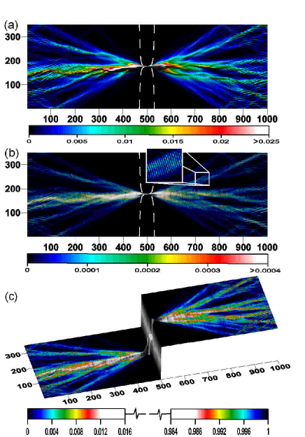
In Fig. 2a, the calculated current density is seen to exhibit a branching behavior that was also apparent in the experiment in Ref. TopinkaNature, . The branched flow is also present in the map of the conductance difference versus the tip position, when the tip is used as a local scatterer (Fig. 2b). It is clear that there is a direct correspondence between the current density calculation and the conductance map. Therefore one can conclude that the experiment in Refs. TopinkaScience, ; TopinkaNature, really probes the current distribution in the sample. Also visible in the conductance difference map are the interference fringes spaced by half the Fermi wavelength (see the inset in Fig. 2b), which were explained as resulting from scattering between the point contact and the STM tip TopinkaScience . The map of the local chemical potential, as measured by the STM voltage probe (Fig. 2c) in this case gives similar information as the previous plots: on the left the current flow appears as regions with increased voltage compared to that of the left lead ( is put equal to zero). This corresponds to a decreased chemical potential due to a deficit of electrons resulting from the non-equilibrium transport process. On the right, the current flow appears as regions with a decreased voltage compared to the right lead. This corresponds to an increased chemical potential (excess electrons due to the transport process).
Small oscillations of the chemical potential with a wavelength on the order of are apparent in Fig. 2c. They result from interference between paths which emerge from the leads and directly enter the probe, and paths which first pass the probe, are reflected from the QPC and only then enter the probe. This effect was already described in Ref. Buttiker2, : the voltage measurement we make is phase sensitive.
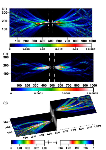
In Fig. 3, the quantities are calculated for the same system as before, but now a magnetic field is included. The field is characterized by a magnetic length of , and a cyclotron radius . From the non-equilibrium transport current density plot (which is symmetric in the magnetic field by its definition in Eqs. 20), it is clear that the branches of electron flow start bending. The radius of curvature has the same order of magnitude as the cyclotron radius, so we are seeing here the onset of the skipping orbit movement of the electrons. The branches are reflected on the upper and lower edges of the sample, a proof that one is still in the ballistic regime.
The conductance difference map (Fig. 3b) is quite unclear. This can be explained as resulting from the reduction of backscattering in the presence of a magnetic field Butt . But nevertheless the tendency of the branches to curve can be observed.
In this regime, the voltage probe method gives better results. The curved branches are clearly visible in Fig. 3c. Please keep in mind that the voltage method is not symmetric under reversal of the field, which results in the asymmetry of the voltage map. This asymmetry will be explained in more detail with the help of Fig. 4c.
In Fig. 4, results are shown for a high magnetic field (magnetic length , cyclotron radius ). In a plot of the transport current density the electrons are seen to describe skipping orbits along the edges of the sample; we are in the quantum Hall regime. In this regime the original tip scattering method fails because of a lack of backscattering Butt . This is visible in Fig. 4b: only in the middle of the quantum point contact there is some conductance decrease because in this region waves travelling in opposite directions are “forced” to overlap. The map of the local chemical potential (Fig. 4c) gives better results: the skipping orbits are clearly visible.
The asymmetry of this plot was already pointed out above, and can be understood as follows: the voltage on the right lead is chosen to be higher than that on the left lead, so electrons are flowing from the left to the right. The magnetic field for this plot is pointing out of the plane of the paper, so electrons emerging from the left lead flow along the upper left edge of the sample, and this edge is in equilibrium with the left lead (no skipping orbits are seen on this edge, only a uniform potential distribution). Some of these electrons are transmitted through the point contact, which results in a higher chemical potential (so lower voltage!) than at the upper right edge of the sample. The electrons reflected from the contact (continuing their path on the lower edge) give rise to a chemical potential that is lower (= voltage that is higher) than () on the lower left edge.
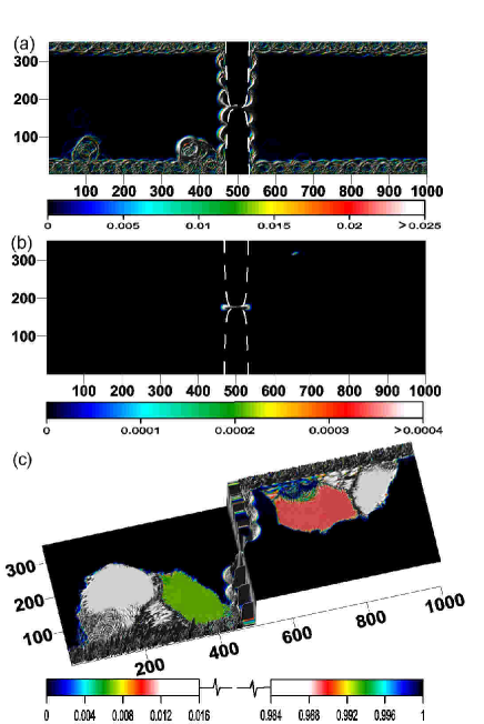
V.2 Two Quantum Point Contacts
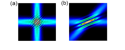
Looking back at the Figs. 2 and 3, another interesting interference effect is taking place, which has not been observed in the experiment. When the branches of electron flow hit the upper and lower border of the sample (in the regions from to and from to on both figures), there are clear interference fringes visible, perpendicular to the border. The wavelength of these fringes is larger than that of the fringes observed in the scatterer experiment (which resulted from back- and forth scattering between the tip and the QPC). This interference pattern can be explained as a crossing of two or more coherent electron beams (branches). In Fig. 5, a simulation is shown where the current density due to two crossing gaussian beams with wavevectors and is calculated. A clear interference pattern is visible, extending in the direction . From comparison between Figs. 5a and 5b, it is clear that the wavelength of the fringes depends on the angle between the two beams. It can be shown that this wavelength is given by:
| (23) |
with , and the angle between the beams.
The different periodicities in the different flow maps can be made more visible by doing a Fourier transformation. In Fig. 6, this is done for columns 1 to 400 of the flow maps in Fig. 2 without a magnetic field. In both maps where an STM is used, a circle with radius centered on can be seen. This circle corresponds to the interference pattern resulting from a superposition of paths between the STM tip and the quantum point contact, which creates the fringes spaced at half the Fermi wavelength. In the current density distribution (Fig. 6c), this circle is of course absent.
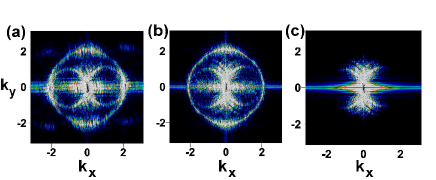
Another feature in Fig. 6 is the presence of two smaller circles centered on the X-axis. They result from the interference effect between crossing beams explained above. Using that the interference pattern of two coherent beams is directed along , together with Eq. 23, these circles can indeed be reproduced by having interference between a main beam directed along the X-axis and others crossing it. While this effect has nothing to do with scattering off the STM tip, these circles are visible in Fourier transforms of all flow maps, including that of the current density distribution.
Now, at crossings between two incoherent beams, an interference pattern like in Fig. 5 will not occur. If one looks at the plot of the transport current with a magnetic field (Fig. 3), one can see that some branches bend upwards, while other bend downwards under influence of the magnetic field. This can be interpreted as follows. In the device, the chemical potential will be somewhere between that of the left and the right lead. If one assumes that the chemical potential on the left lead is larger than that on the right, we have an excess of electrons flowing from left to right. On the other hand we have a deficit of electrons (“holes”) flowing the other way. These electrons and holes bend in opposite ways under influence of a magnetic field, because they fill different scattering states. It is clear then that electrons and holes, and thus branches curving upwards and downwards, are emerging from different reservoirs and are thus phase incoherent. As a result, one does not expect to see interference between beams with different chirality.
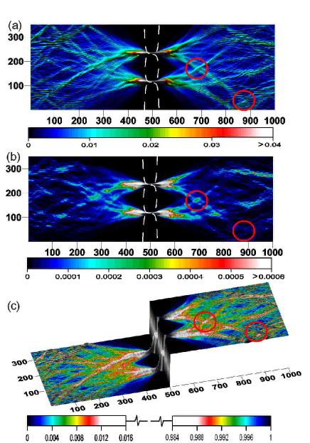
In order to test this statement, we have made some calculations for a system of two QPC’s placed above each other. The potential of both QPC’s has the same form as in Eq. 22, and all parameters are chosen as in Fig. 3. The results are shown in Fig. 7. Under influence of the magnetic field, the branches are curved. One can clearly see the interference between beams with the same chirality, but there is no interference at the crossing of two beams with opposite chirality, like we expected. This distinction becomes clear when comparing the crossings that are encircled in Fig. 7. To make things more clear, we have smoothed out the interference fringes in Fig. 7b) resulting from scattering between tip and QPC which had a wavelength of . In Fig. 7c, we symmetrized the voltage probe plot with respect to the direction of the magnetic field. Also in this plot, the behavior for coherent beams crossing is different from that for incoherent branches. This proves that the effect could be studied experimentally.
VI Conclusion
We have established an efficient tight-binding method to numerically calculate spatial maps of electron flow as obtained in a recent series of scanning probe experiments where an STM tip is used as a local scatterer for electrons TopinkaScience . The computational effort of our numerical approach scales like (in the limit ), where is the width of the lattice and is the length. It is in this way more efficient than the standard recursive Green’s function method which scales like for the same problem.
We have also shown expressions for the local density of states, the electron density and the current density distribution. These quantities cannot be calculated within the standard recursive approach, but within our scheme they can be expressed in terms of the same Green’s functions already known from the numerical simulation of the scanning probe experiment. The computational effort for these quantities also scales as .
When a magnetic field is applied, backscattering of electrons will be strongly reduced because of the presence of edge states so that the original STM method does not give the desired results. Therefore, a probe method was proposed where the tip is used to measure the local chemical potential. For this problem again, the numerical effort scales like . The image one obtains from such a method is not always directly related to the current pattern in the sample, but one can expect to obtain relevant information about transport in the sample.
The power of the method was proven in example calculations, where a tight-binding lattice with more than sites has been used. Moreover, by direct comparison between a numerical simulation of the experiment and a calculation of the exact current density distribution, it became clear that the original scanning probe technique of Topinka et al. TopinkaScience is really imaging current flow. Furthermore, a new interference phenomenon has been observed which resulted from the crossing of phase coherent branches, and a new setup with two QPC’s has been discussed to distinguish between crossings of coherent branches and incoherent ones. This distinction is visible both when the tip is used as a scatterer, and when it is used as a voltage probe, so that an experimental investigation of the effect should be possible.
It should be clear that the method proposed is very general, and the information obtained by the different imaging tools very broad, so that it can be used to study electron flow in a variety of systems ranging from e.g. the quantum Hall effect to quantum chaos in electron billiards Marcus . Moreover, including the spin degrees of freedom proves to be rather easy; every matrix element should be replaced by a spinor. As such, an even broader range of phenomena could be studied, ultimately also those including spin-orbit coupling (e.g. the spin Hall effect Hirsch ; Sinova ).
Appendix A Calculation of Green’s Functions relevant to our Problem
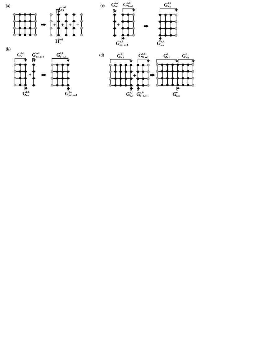
In the paper, it became clear that indeed all quantities we need can be expressed in terms of a small subset of Green’s functions , , and (see Fig. 1). In this appendix, we will treat in detail how to obtain these functions with a numerical effort that scales like .
The first step is to divide the central device into its separate columns, and to put the hopping matrices between them equal to zero so that the columns become isolated, as depicted in Fig 8a. Next, one calculates the Green’s function for every isolated column , which amounts to doing a single matrix inversion. This first step thus needs a total of inversions.
The next step is to attach the isolated columns one by one to each other by including the hopping matrices between them using Dyson’s equation (this is like in the standard recursive technique, see e.g. Ref. Ferry, ). As such, one calculates the Green’s functions and (see Fig. 8b). Please note that since not all columns are attached to each other in and (only those to the left of column ), these Green’s functions are not equal to the Green’s functions and we are trying to obtain (an exception of course is which in fact is equal to ). The superscript L is added to make this distinction clear.
Attachment of a single isolated column costs one inversion of an matrix, so a total of matrix inversions are necessary to calculate the and for all , starting from the .
For the third step, we start over from the isolated Green’s functions already calculated in step 1, and glue them together like we did in the previous step on the basis of a Dyson’s equation, but now beginning from the right, like depicted in Fig. 8c. The Green’s functions we calculate with every step are , and . Again, a single matrix inversion is needed for the attachment of a single column, so a total of inversions for the completion of the third step.
The final step is to get the , , and we are looking for by attaching the previously calculated Green’s functions in pairs, like illustrated in Fig. 8d. One takes a section of connected columns to (with known Green’s functions and ), and attaches it to the section of connected columns to (with Green’s functions and ). Please note that a single inversion is necessary for each pairwise addition, which gives a total of inversions for the final step.
From the previous discussion, it becomes clear that we need inversions for calculating , , and for all . So our method scales indeed linear with in the number of inversions.
Appendix B Evaluation of the Trace
For the scatterer method, it is necessary to calculate the conductance difference in Eq. 9. For this, it seems that we have to evaluate the trace in Eq. 10 for all tip positions. This trace contains products of matrices, so the numerical effort for this step would scale like . As such one would loose a factor of in efficiency compared to the rest of the calculation. However, there is a better way to evaluate the conductance difference in Eq. 9.
We write (see Eq. (13)):
| (24) |
with the matrix:
| (25) |
It is important now to make it clear that since has only one non-zero element, namely on position , one can write as a product of a column matrix and a row matrix:
| (26) |
with the scalar given by ( is the magnitude of the repulsive tip potential):
| (27) |
By substituting Eq. (24) into Eq. (10), one obtains:
| (28) |
So in order to evaluate the conductance difference , we need to evaluate only the last two terms in Eq. (28). The last term only involves products of an matrix with row or column matrices because of the special form of . The computational effort for this term scales thus as , which corresponds to a total effort of for all tip locations. Now, since is independent of the tip position, it has to be calculated only once (with an effort ). When this matrix is known, the trace in the second term also contains only products of an matrix with a row or column matrix, so the computational effort then scales like , and as a result the effort for all tip positions scales like in the limit of large . As such, we do not loose our efficiency.
References
- (1) S. Datta, Electronic Transport in Mesoscopic Systems, (Cambridge University Press, England, 1995).
- (2) D. K. Ferry and S. M. Goodnick, Transport in Nanostructures, (Cambridge University Press, England, 1997).
-
(3)
B. J. van Wees, H. van Houten, C. W. J. Beenakker,
J. G. Williamson, L. P. Kouwenhoven , D. van der Marel, and
C. T. Foxon, Phys. Rev. Lett. 60, 848 (1988).
D. A. Wharam, T. J. Thornton, R. Newbury, M. Pepper, H. Ahmed, J. E. F Frost, D. G. Hasko, D. C. Peacock, D. A. Ritchie, and G. A. C. Jones, J. Phys. C 21, L209 (1988). - (4) K. von Klitzing, G. Dorda, and M. Pepper, Phys. Rev. Lett. 45, 494 (1980).
- (5) P. A. Lee, A. D. Stone, and H. Fukuyama, Phys. Rev. B, 35, 1039 (1987).
- (6) M. A. Topinka, B. J. LeRoy, S. E. J. Shaw, E. J. Heller, R. M. Westervelt, K. D. Maranowski, and A. C. Gossard, Science 289, 2323 (2000).
- (7) M. A. Topinka, B. J. LeRoy, R. M. Westervelt, S. E. J. Shaw, R. Fleischmann, E. J. Heller, K. D. Maranowski, and A. C. Gossard, Nature 410, 183 (2001).
- (8) B. J. LeRoy, J. Phys.: Condens. Matter 15, R1835 (2003).
- (9) G.-P. He, S.-L. Zhu, and Z. D. Wang, Phys. Rev. B 65, 205321 (2002).
- (10) M. Büttiker, Phys. Rev. Lett. 57, 1761 (1986).
- (11) M. Büttiker, Phys. Rev. B 38, 9375 (1988).
- (12) P. Muralt and D. W. Pohl, Appl. Phys. Lett. 48, 514 (1986).
- (13) J. R. Kirtley, S. Washburn, and M. J. Brady, Phys. Rev. Lett. 60, 1546 (1988).
- (14) T. Gramespacher, M. Büttiker, Phys. Rev. B 56, 13026 (1997).
- (15) T. Gramespacher, M. Büttiker, Phys. Rev. B 60, 2375 (1999).
- (16) R. E. Peierls, Z. Phys. 80, 763 (1933).
- (17) D. Guan, U. Ravaioli, R. W. Giannetta, M. Hannan, I. Adesida, and M. R. Melloch, Phys. Rev. B 67, 205328 (2003).
- (18) M. P. Lopéz Sancho, J. M. Lopéz Sancho, and J. Rubio, J. Phys. F 15, 851 (1985).
- (19) I. Turek, V. Drchal, J. Kudrnovský, M. S̆ob, and P. Weinberger, Electronic structure of disordered alloys, surfaces and interfaces, (Kluwer, Boston, 1997).
- (20) A. Cresti, R. Farchioni, G. Grosso, and G. P. Parravicini, Phys. Rev. B 68, 075306 (2003).
- (21) J. H. Davies, The physics of low-dimensional semiconductors : an introduction, (Cambridge University Press, Cambridge, 1998).
- (22) M. Büttiker, Phys. Rev. B 40, R3409 (1989).
- (23) C. M. Marcus, A. J. Rimberg, R. M. Westervelt, P. F. Hopkins, and A. C. Gossard, Phys. Rev. Lett. 69, 506 (1992).
- (24) J. E. Hirsch, Phys. Rev. Lett. 83, 1834 (1999).
- (25) J. Sinova, D. Culcer, Q. Niu, N. A. Sinitsyn, T. Jungwirth, and A. H. MacDonald, Phys. Rev. Lett. 92, 126603 (2004).