Long-range ordering of III-V semiconductor nanostructures by shallowly buried dislocation networks
Abstract
We account for lateral orderings of III-V nanostructures resulting from a GaAs/InAs/InGaAs/GaAs sequence grown on GaAs by metalorganic vapour phase epitaxy at two different temperatures. For both samples, the ordering is induced by the stress field of a periodic dislocation network (DN) shallowly buried and parallel to the surface. This DN is a grain boundary (GB) that forms, between a thin GaAs layer (on which growth was performed) and a GaAs substrate joined together by wafer bonding, in order to accommodate a tilt and a twist between these two crystals; both these misorientations are imposed in a controlled manner. This GB is composed of a one-dimensional network of mixed dislocations and of a one dimensional network of screw dislocations. For both sample, the nanostructures observed by transmission electron microscopy (TEM) and atomic force microscopy are ordered by the underlying DN observed by TEM since they have same dimensions and orientations as the cells of the DN.
pacs:
61.72.Lk 61.72.Mm 68.37.Lp 68.65.-k1 Introduction
The control on a wide surface of the size, position and density of self-assembled quantum dots (QDs) is a requirement for the increase of the performances of numerous optoelectronic devices, such as semiconductor lasers, or for the realization of new devices, such as a single photon source for quantum information based on an isolated QD. One way to achieve this control is to use the periodic stress field induced at the surface of a specimen by a periodic dislocation network (DN) shallowly buried and parallel to the surface, which generates preferential nucleation sites for the QDs [1, 2]. So, by choosing an adequate periodicity, it should be possible to organize laterally QDs with identical sizes. Here we study two samples for each of which a shallowly buried DN accommodates crystallographic misorientations imposed in a controlled manner between two GaAs crystals (a substrate and a thin layer) joined by wafer bonding. This method has the outstanding property of no leading to the formation of any threading dislocation which could affect the optical properties of the subsequently grown layers [5]. Moreover, since the charge carriers are strongly confined in QDs, the optical sensitivity of the latter to the presence of defects (such as the dislocations of an underlying DN) should be weak [6]. Till now, lateral ordering of nanostructures mediated by an underlying DN has been reported for metals [3] and for Germanium on Silicon [4] but not for III-V materials. Here, we report a major step towards the long-range lateral organization of III-V self-assembled QDs, namely long-range lateral organizations of III-V nanostructures induced by the buried DNs previously reported. Growth was performed at different temperatures on two samples, for which, the periodicities of the DNs are also different.
2 Experimental procedure
At the interface between two crystals, a grain boundary (GB) forms. This GB is constituted of a periodic DN that accommodates the crystalline discontinuity. Thus, to obtain a shallowly buried DN, we transfer by wafer bonding a thin crystalline GaAs layer on a host GaAs substrate, between which we impose controlled misalignments of their reticular planes (to be detailed below). We called the resulting structure a ‘composite substrate’.
First the thin layer (approximately 20 nm thick) is grown by metalorganic vapour phase epitaxy (MOVPE) on a sacrificial GaAs substrate. Two Al0.9Ga0.1As etch-stop layers separated by a GaAs buffer layer are also grown between the thin GaAs layer and the sacrificial substrate in order to allow the removal of the latter (as well as the AlGaAs layers) by wet selective chemical etching after the bonding. We use two etch-stop layers rather than only one to better control the removal of the sacrificial substrate and obtain a surface as smooth as possible.
After cleaning and deoxidizing, this structure and the host substrate are superposed with controlled crystalline misalignments imposed between them. These misalignments are a twist (i.e. a rotation around an axis orthogonal to the interface) and a tilt (i.e. a rotation around an axis lying in the interface). The tilt is established by using commercial vicinal wafers: their surfaces are disoriented by , around an in plane direction, with respect to the (001) plane. On the other hand, to control the twist, we first cut with a saw square pieces of a wafer to obtain sides having the desired disorientation with respect to the 110 cleavage directions. We then put in contact and align the sides of a sawn square and of a square simply cleaved along the 110 directions – these two squares are the crystals that will be bonded. This method allows twist control to within . Considered independently, a twist between two crystals is accommodated by a square two-dimensional (2D) network of screw dislocations, while a tilt is accommodated by a one-dimensional (1D) network of mixed dislocations oriented along the tilt axis (the line orthogonal to the maximum slope of the interface). The two crystals were superposed so that the maximum slope of their surfaces are orthogonal and thus the resulting maximum slope of the interface is along a direction. For these two DNs, the periodicity is:
| (1) |
where is the modulus of the Burgers’ vector component allowing the accommodation of the misorientation considered and is the misorientation angle. In III-V materials, for screw dislocations, is the entire modulus of the Burgers vector, equal to (where is the lattice parameter of the material), while for mixed dislocations it is the Burger’s vector component normal to the boundary plane: .
Afterwards, this stack is annealed during one hour, at 600∘C, under nitrogen flow. During this heating, a mechanical pressure (between 10 and 100 kg/cm2) is applied on the stack in order to maintain the surfaces of the two crystals in contact. Indeed, contrary to Si/Si bonding for example, deoxidized and flat GaAs surfaces do not bond at room temperature when they are simply put in contact. On the other hand, the difficulty to impose a homogeneous pressure on a wide surface limits the dimensions of our composite substrates. However, we succeeded to increase their surface area from 1 cm2 to 4 cm2. During the annealing, covalent bonds form at the bonding interface, while a DN forms to accommodate the misalignments.
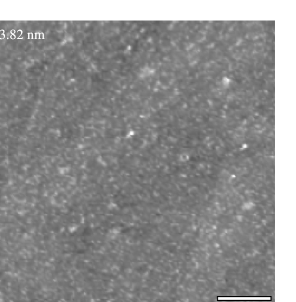
After, the sacrificial GaAs substrate is mechanically thinned and then etched by a stirred citric acid solution obtained by dissolving 50 g of citric acid in 50 cm3 of deionized water and adding 20 cm3 of 30% H2O2. On the other hand, the AlGaAs layers are eliminated with a 5% hydrofluoric solution, to leave only the thin GaAs layer bonded to the host substrate. Figure 1 illustrates the typical resulting surface. It is very flat: the root mean square (RMS) roughness of 0.28 nm is similar to that of regular GaAs substrates. Notice that for the chemical etchings to be selective it is important that the etched materials be undoped.
Finally, on two such composite substrates, after a 9 min annealing at 650∘C which purpose was to evaporate the surface oxide, we deposited by MOVPE a III-V multilayer that gives rise on regular substrate to the formation of QDs [7], in order to observe the effect, on this growth, of the strain field of the buried DN. The growth sequence was GaAs/InAs/In0.15Ga0.85As/GaAs. It was performed at 470 ∘C (sample A) or 450∘C (sample B).
3 Results and discussion
Cross-section transmission electronic microscope (TEM) observations of the structures showed that they are different from those obtained on regular substrates (the phenomenon is illustrated in figure 2 for sample A).
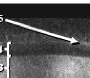
Starting from the bottom, we find the host GaAs substrate (#1) and the bonded GaAs layer (#2). Their interface is the GB, where the large dark spots are due to the strain fields around the dislocations and the small ones to cavities (resulting from the non planarity of the surfaces put in contact) or to segregated impurities. As expected, the dislocations remain confined to the GB and do not propagate in the surrounding layers. The grown layers are above layer #2. No QD is observed in this sample. Nevertheless, both the GaAs buffer layer (#3) and the InGaAs alloy layer (#4; which results from the intermixing between the InAs and In0.15Ga0.85As deposited layers) exhibit thickness modulations, to be discussed below. Finally, a thin GaAs layer (#5) covers the entire structure (the weak contrast above the latter is due to glue). The presence of a dark line at the #2/#3 GaAs/GaAs homointerface might seem surprising. However, the top of layer #2, on which growth is started, is obtained by chemical etching and cannot have the quality of standard ‘epi-ready’ wafers. Moreover, secondary ion mass spectroscopy shows that impurity levels as low as 1018 cm-3 suffice to produce such features. Finally, from the image intensity ratio between the InxGa1-xAs and the GaAs in figure 2, and using our previous work [10], we determined the average indium composition of layer #4: x=0.310.02.
From such images, it appears readily that the thickness modulations, which affect both the GaAs buffer and the InGaAs layer, are not randomly distributed: for instance, thicker InGaAs grows in the valleys of the GaAs layer. Since moreover their dimensions, modulation periods and modulation amplitudes are of the order of between 1 and 100 nm, these features truly constitute III-V semiconductor nanostructures. These nanostructures are clearly the direct effect of the underlying dislocations during growth, and are not mediated by a possible undulation of the initial growth surface, namely the top of layer #2; indeed, as was shown in figure 1, the latter exhibits a negligible non-ordered corrugation. However, cross-sections such as figure 2 allow a detailed study neither of their organization nor of the relationship between the underlying dislocations and the nanostructures.
Figure 3 is a TEM plan-view of sample A, obtained with diffraction vector g along a direction. Such imaging condition reveals chiefly the high strain field localized close to the dislocation cores for which g.b is not zero and not the more diffuse strain field associated with the thickness modulations of the GaAs and InGaAs layers. The interface cavities are also imaged; though many of them seem to deviate and pin the dislocations, their distribution is random and homogenous (in particular, it is not related to the periodicities of the dislocations). On the other hand, weak beam images formed with the orthogonal reflection seem to show only the same dislocations. TEM plan-views taken with the same imaging conditions on sample B reveal a similar grain boundary, with slightly different periodicities (to be detailed below).
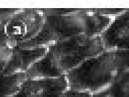
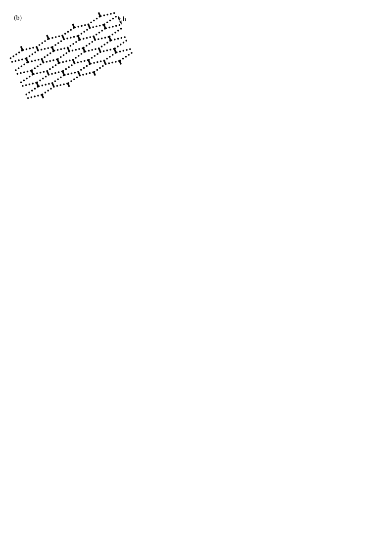
From detailed observations on similar DNs samples (to be reported elsewhere), we could identify the DNs of the present GBs. They are constituted of a 1D network of screw dislocations shifted, perpendicularly to their line direction, by approximately half a period each time it crosses a dislocation of the orthogonal 1D network of mixed dislocations (a schematic representation of figure 3 is shown in figure 3). For sample A, the period of the screw DN is nm, corresponding to a twist of , and that of the mixed DN is nm, corresponding to a tilt of . For sample B, the period of the screw DN is nm, corresponding to a twist of , and that of the mixed DN is nm, corresponding to a tilt of . All these experimental values are in agreement with the expected ones. The shifts of the screw dislocations, as well as the saw-tooth aspect of the mixed dislocations, arise from energy minimizing interactions [8, 9]. The resulting dislocations cells are roughly hexagonal. The long dimension of these cells is exactly the period of the screw DN and the short dimension is (figure 3): for sample A and nm for sample B.
So, whereas we expected for both samples a 2D network of screw dislocations allowing to accommodate the twist, here we only observe a 1D DN. From the detailed studies of our other DNs that allowed us to identify the dislocations of the present samples, we could prove that when the mixed dislocations are approximately oriented along a 110 direction (like the screw dislocations), they accommodate part of the twist by means of their Burgers vector screw components (that will be detailed elsewhere). For both samples, we observed such mixed dislocations. Moreover, since for both cases the mixed dislocations are more than two times more numerous than the screw dislocations and though they are two times less efficient than the latter to accommodate a twist (their Burgers vector screw components are two times lower than those of the latter), it is possible that they ‘replace’ the missing 1D screw DN and accommodate the entire remaining twist. With respect to interface energy, it seems highly favorable to eliminate totally one half of the standard 2D screw DN.
Whereas AFM images of composite substrates before growth reveal only a flat non-ordered surface (figure 1), AFM observations on samples A and B after growth (figure 4) reveal the presence of nanostructures.
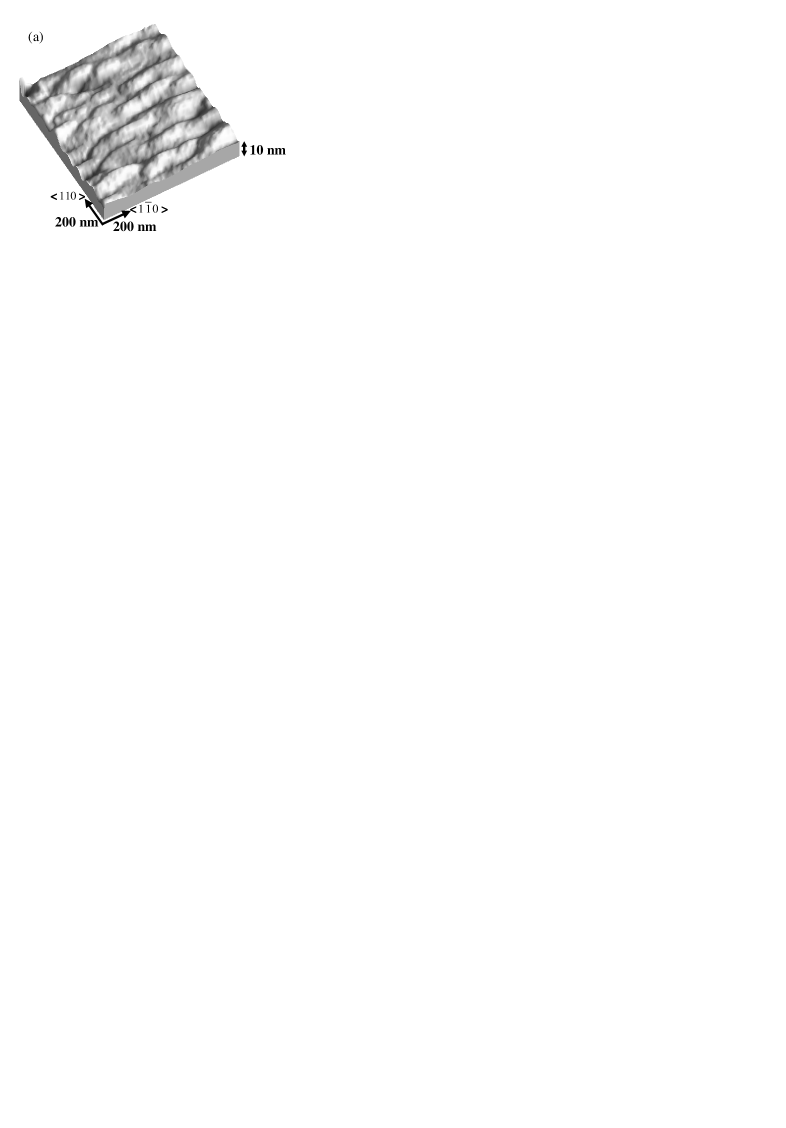
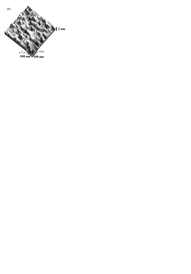
These nanostructures result from the superposition of the GaAs and InGaAs nanostructures observed in the cross-section. However since the GaAs nanostructures are higher than the InGaAs ones, the nanostructures observed in figure 4 are certainly mostly due to the former. These surface nanostructures are elongated along a 110 direction like the cells of the underlying DNs. Moreover, for both samples, their lateral dimensions, measured by height profiles taken along the 110 directions, are identical to those of the DN cells (to within experimental uncertainties). So, for both samples, though the periodicities of their DNs and the growth temperatures are different, the nanostructures are ordered by these shallowly buried DNs.
By comparing the two images of figure 4 and though they have different scales (adapted to the different dimensions of the nanostructures), we notice that the surface nanostructures of sample A seem flatter than those of sample B. We expected such a difference; indeed, for the latter sample, the growth temperature was lowered by 20∘C in order to diminish the diffusion length of atoms and favour the formation of less flat nanostructures, our aim being to approach the aspect of conventional QDs. However, the mean height of these nanostructures is lower than for sample A: 1 nm, against 2 nm for the latter. This lower value for sample B is not surprising and results from the lower period of the DN: when dislocations approach each other, i.e. when the DN period is reduced, the stress induced at the surface is reduced because of a screening effect [1]. In order to determine with certainty which of the samples really has flatter surface nanostructures, we assimilated the nanostructures bases to ellipses and calculated the ratios between their heights and their bases areas. For sample A, the average of these ratios is nm-1 while for sample B it is nm-1, that is 1.6 times higher than for sample A. So the surface nanostructures of sample B are indeed less flat than those of sample A.
4 Conclusion
We managed to order III-V nanostructures with the stress field of periodic shallowly buried DNs. These nanostructures consist of modulations of GaAs and InGaAs layers due to the stress field of the dislocations. Moreover, we demonstrated that by modifying the growth conditions (namely, by reducing the growth temperature), we can obtain less flat nanostructures. It is a very encouraging result in the perspective of ordering QDs for applications to optical emitters. Such ordered QDs should be formed by further reducing the size of the DN cells, which should lead to the reduction of the lateral dimensions of the nanostructures.
References
References
- [1] Bourret A 1999 Surf. Sci. 432 37
- [2] Romanov A E, Petroff P M and Speck J S 1999 Appl. Phys. Lett. 74 2280
- [3] Brune H, Giovannini M, Bromann K and Kern K 1998 Nature 394 451
- [4] Leroy F, Eymery J and Gentile P 2002 Appl. Phys. Lett. 80, 3078
- [5] Liau Z L and Mull D E Appl. Phys. Lett. 56, 737 (1990).
- [6] Gérard J M, Cabrol O and Sermage B 1996 Appl. Phys. Lett. 68, 3123
- [7] Saint-Girons G, Patriarche G, Largeau L, Coelho J, Mereuta A, Gérard J M and Sagnes I 2002 J. Cryst. Growth 235, 89
- [8] Hirth J P and Lothe J 1982 Theory of Dislocations 2nd edition (New York: Wiley) p 660
- [9] Benamara M, Rocher A, Laporte A, Sarrabayrousse G, Lescouzères L, PeyreLavigne A, Fnaeich M and Claverie 1995 A Matter. Res. Soc. Symp. Proc. 378, 863
- [10] Patriarche G, Largeau L, Harmand J C and Gollub D Appl. Phys. Lett. 84, 203 (2004).