Modeling of Inelastic Transport in One-dimensional Metallic Atomic Wires
Journal of Computational Electronics X:YYY-ZZZ,200?
©Kluwer Academic Publishers Manufactured in The Netherlands
Modeling of Inelastic Transport in One-dimensional Metallic Atomic Wires
THOMAS FREDERIKSEN, MADS BRANDBYGE, ANTTI–PEKKA JAUHO
MIC –
Department of Micro and Nanotechnology, Technical University of Denmark,
Ørsteds Plads, Bldg. 345E, DK-2800 Lyngby, Denmark
thf@mic.dtu.dk
NICOLÁS LORENTE
Laboratorie Collisions, Agrégats,
Réactivité, IRSAMC, Université Paul Sabatier,
118 Route de Narbonne, F-31062 Toulouse, France
Abstract. Inelastic effects in electron transport through nano-sized devices are addressed with a method based on nonequilibrium Green’s functions (NEGF) and perturbation theory to infinite order in the electron-vibration coupling. We discuss the numerical implementation which involves an iterative scheme to solve a set of coupled non-linear equations for the electronic Green’s functions and the self-energies due to vibrations. To illustrate our method, we apply it to a one-dimensional single-orbital tight-binding description of the conducting electrons in atomic gold wires, and show that this simple model is able to capture most of the essential physics.
Keywords: Inelastic transport, nonequilibrium Green’s functions, self-consistent Born approximation.
1. Introduction
Atomic-size conductors represent the ultimate limit of miniaturization, and understanding their properties is an important problem in the fields of nanoelectronics and molecular electronics. Quantum effects become important which leads to a physical behavior fundamentally different from macroscopic devices. One such effect is the inelastic scattering of electrons against lattice vibrations, an issue which is intimately related to the important aspects of device heating and stability.
In this paper we describe a method to calculate the inelastic transport properties of such quantum systems connected between metallic leads. As a specific example, we here apply it to a simple model for atomic Au wires, for which such inelastic signals have recently been revealed experimentally [1].
2. Inelastic transport formalism
Our starting point is a formal partitioning of the system into a left () and a right () lead, and a central device region (), in such a way that the direct coupling between the leads is negligible. Hence we write the electronic Hamiltonian as
| (1) |
where is a one-electron description of lead and the coupling between and . The central part is also a one-electron description but depends explicitly on a displacement vector corresponding to mechanical degrees of freedom of the underlying atomic structure in this region (within the Born-Oppenheimer approximation we assume instantaneous response of the electrons). We are here concerned with the electronic interaction with (quantized) oscillatory motion of the ions. For small vibrational amplitudes the -dependence can be expanded to first order along the normal modes of the structure, i.e.
| (2) | |||||
| (3) | |||||
| (4) |
where () is the single-electron creation (annihilation) operator and () the boson creation (annihilation) operator. The ionic Hamiltonian is just the corresponding ensemble of harmonic oscillators
| (5) |
where is the energy quantum associated with .
The transport calculation is based on NEGF techniques [2]. For steady state the electrical current and the power transfer (per spin) to the device from lead is given by [3]
| (6) | |||||
| (7) | |||||
| (8) |
where is the electronic number operator of lead . Above we have introduced Green’s functions in the device region and the lead self-energies (scattering in/out rates) due to lead . For a shorthand notation these are written as matrices in the -basis. For example, the elements in are the Fourier transforms of . In the limit of zero coupling , we can solve exactly for the lead self-energies and the device Green’s functions (since this is a single-electron problem).
Complications arise with a finite coupling, where the vibrations mediate an effective electron-electron interaction. To use Eq. (6) and (7) we need the “full” Green’s functions . Our approach is the so-called self-consistent Born Approximation (SCBA), in which the electronic self-energies due to the phonons are taken to lowest order in the couplings [2]. For a system lacking translational invariance [3]
| (9) | |||||
| (10) | |||||
In the above, the phonon Green’s functions are approximated by the noninteracting ones [2]. Finally, are related to , , and via the Dyson and Keldysh equations [2]
| (11) | |||||
| (12) |
The coupled non-linear equations (9)–(12) have to be solved iteratively subject to some constraints on the mode population (appearing in ). We identify two regimes: (i) the externally damped limit where the populations are fixed according to the Bose distribution , and (ii) the externally undamped limit where the populations vary with bias such that no power is dissipated in the device, i.e. . To solve the above we have developed an implementation in Python, in which the Green’s functions and self-energies are sampled on a finite energy grid.
3. Simple model
As a simple illustration of our method, let us consider an infinite one-dimensional single-orbital tight-binding chain. We define the central region to be a piece of it with sites to represent the conducting electrons in a finite metallic atomic wire. The two semi-infinite pieces which surround can now be considered as left and right leads. Ignoring on-site energy and hopping beyond nearest neighbors we simply have for
| (13) |
The hopping amplitudes explicitly depend on the displacement vector where the coordinate describes the displacement of ion from its equilibrium position. As a specific model for the hopping modulation by displacement we use the so-called Su-Schrieffer-Heeger (SSH) model [4] in which the hopping parameter is expanded to first order in the intersite distance
| (14) |
where and are site-independent parameters. To describe the ions (in a uniform chain where the end sites are fixed in space, ) we include only nearest neighbor springs and write
| (15) |
where is the ionic mass and the effective spring constant between two neighboring sites.
Imposing quantization via , we can formulate the linearized electron-vibration interaction in terms of the normal mode operators and ,
| (16) |
and relate the coupling elements to components of the normal mode vectors (normalized ) as [3]
| (17) |
It is well established that atomic Au wires have one almost perfectly transmitting eigenchannel at the Fermi energy (e.g. [1] and references herein). To avoid reflection in our model we describe the leads with the same electronic parameters as for the wire, leading to semi-elliptic band structures of the leads with widths . With one electron per site the band is half filled and the Fermi energy becomes . Further, we take the lead states to be occupied according to Fermi distributions where the chemical potentials vary as and . With this information we essentially have [3]. The setup and the set of normal modes for a particular atomic wire are shown in Fig. 3..

4. Numerical results
Let us now discuss our numerical results for the differential conductance calculated with Eq. (6) for different lengths and spring constants . We use the parameter values stated in Tab. 4. which qualitatively yields reasonable agreement with the experimental measurements on atomic Au wires [1].
| Physical quantity | Symbol | Value |
|---|---|---|
| Bare hopping | 1.0 eV | |
| Hopping modulation | 0.6 eV/Å | |
| Fermi energy | 0.0 eV | |
| Atomic mass | 197 a.m.u. | |
| Spring constant | 2.0-8.0 eV/ | |
| Temperature | 4.2 |
The linear energy grid in principle has to cover the full bandwidth (FBW) while at the same time it must have a resolution fine enough to sample and well. For this model, to resolve the fastest variations (caused by the Fermi function) the grid point separation should be around meV or better at a temperature of . We find that calculations carried out on an interval converge quickly with to those of the FBW. As we show below for a few representative cases, complete agreement is found when eV (which hence are used in the calculations presented here). Over this narrow range we can further apply the wide band limit (WBL) . These simplifications reduce the computational load significantly.
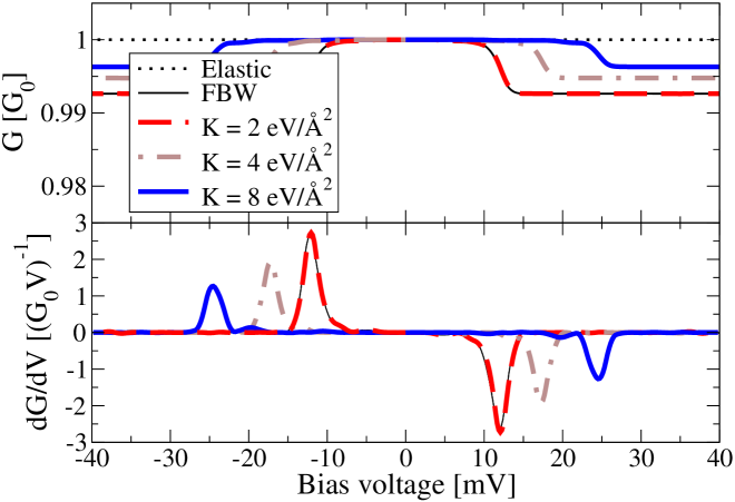
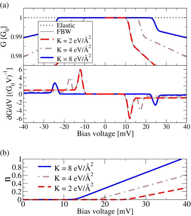
The nonlinear conductance versus applied bias across a 6-atom wire is shown (i) for the externally damped limit in Fig. 4. and (ii) for the externally undamped limit in Fig. 4.. It is seen from Fig. 4. that the conductance drop essentially happens at one particular threshold energy. This energy is found to coincide with that of the mode with highest vibrational energy, i.e. the mode with alternating bond length (ABL) character, which can also be designated as the dominating one. This mode is further studied in the externally undamped limit, Fig. 4., in which a finite slope is observed beyond the threshold as well as a linear increase in the mode population with bias (heating). Generally, both figures show that the conductance drop increases while the phonon threshold decreases when the spring constant is lowered. This can be interpreted as an effect of straining the wire which cause the bonds to weaken. Notice also the agreement in both figures between the FBW and the WBL calculations, shown for the case eV/.
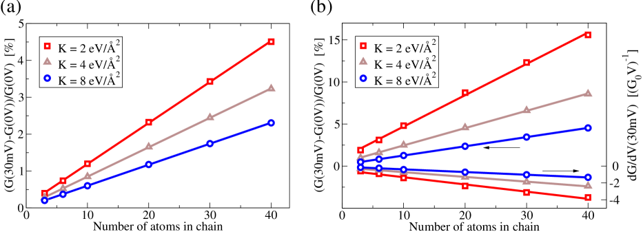
With our simple model we can easily handle longer wires. In Fig. 4. we show a compilation of the conductance drops and the conductance slopes for wires with length up to . The individual conductance plots all look quantitatively much like those of Fig. 4. and 4.. The important result is that these quantities scale linearly with . If one plots the conductance drop against the inverse of mode energy (say, of the dominating mode) it is found that the conductance drop also scales with as (for fixed ), as one could speculate from Eq. (17).
5. Conclusions
In conclusion, we have described a method to calculate inelastic transport properties of an atomic-sized device connected between metallic leads, based on NEGF techniques and SCBA for the electron-vibration coupling. As a numerical example, we studied a simple model for the transport through atomic Au wires. With a single-orbital tight-binding description we illustrated the significance of ABL mode character, and were able to explore even very long wires. We further discussed the approximations related to a representation on a finite energy grid.
As a final remark, and as we show elsewhere [5], the described method is also well suited for a combination with full ab initio calculations. The authors thank M. Paulsson for many fruitful discussions.
References
- [1] N. Agraït, C. Untiedt, G. Rubio-Bollinger, and S. Vieira, “Onset of Energy Dissipation in Ballistic Atomic Wires,” Phys. Rev. Lett. 88, 216803 (2002).
- [2] H. Haug and A.–P. Jauho, “Quantum Kinetics in Transport and Optics of Semiconductors,” Springer (1996).
- [3] T. Frederiksen, “Inelastic electron transport in nanosystems,” Master’s thesis, Technical University of Denmark (2004).
- [4] W. P. Su, J. R. Schrieffer, and A. J. Heeger, “Solitons in Polyacetylene,” Phys. Rev. Lett. 42, 1698 (1979).
- [5] T. Frederiksen, M. Brandbyge, N. Lorente, and A.–P. Jauho, “Inelastic scattering and local heating in atomic gold wires,” submitted for publication, cond-mat/0410700.