Microscopic Model for a Strongly Correlated Superconducting Single-Electron-Transistor
Abstract
We model a Superconducting Single-Electron Transistor operating by repulsive interactions. The device consists of a ring of Hubbard clusters, placed between electrodes and capacitively coupled to a gate potential. In each cluster, a pair of electrons at appropriate filling feels a weak effective interaction which leads to pairing in part of the parameter space. Thus, the system can host many bound pairs, with correlation induced binding. When the charging energy exceeds the pairing energy, single-electron tunneling prevails; in the opposite regime, we predict the Coulomb blockade pattern of two-electron tunneling. This suggests that in tunneling experiments repulsion-induced pairs may behave in a similar way as phonon-induced ones.
pacs:
73.23.-b, 73.40.Gk, 81.07.NbI Introduction
In recent years, a variety of transport experiments have been reported in molecular size systems, such as quantum dots and nanotubes, as a contribution to the current boost towards of the progress in nanoscale technology. From the theoretical side, circuits of several kinds have been modeledaligia , and in applied electronics the Single-Electron-Transistorsrevmodphys are among the most important devices. These are realized by connecting a nanoscopic conducting island to metallic leads and to a gate voltage. The energy gaps existing between states with different number of particles allow to fix the number of electrons in the island very sharply; as a consequence single electrons can tunnel to or from the conductor. Even more appealing situations arise when the above scenario is complicated by electron-electron interactions, as in the case of a Superconducting-Single Electron Transistor (S-SET).
A S-SET is a mesoscopic device obtained by linking capacitively a superconducting grain to two normal leads and to a gate electrode as welldefinizione . The latter allows one to control the number of electrons on the grain by tuning the gate voltage . Such a system has been studied both experimentallydevoret and theoreticallyaverin hekking hanke in great detail during the past years. In a normal island the parity of oscillates between even and odd values, by varying ; conversely in a superconducting island is always even because of the paired nature of the ground state. Therefore the S-SET transport properties in the linear regime are governed by Andreev reflection under the critical temperature of the central island, while above single electron tunneling prevails. This leads to well pronounced Coulomb blockade peaks of the conductance as a function of the gate voltage. In particular the parity-controlled tunneling produces periodic peaks in the pair-tunneling regime, in contrast with the periodicity of the normal system (here is the capacity of the gate electrode). This behavior is well reproduced by models averin hekking hanke using a gate controlled BCS Hamiltonian ; the connection to free electron leads employs a tunneling Hamiltonian, usually treated by second-order perturbation theory.
In the present article we propose a model for a S-SET with a strongly correlated, repulsive Hubbard-like model instead of as the “superconducting” grain Hamiltonian. That is, we look for a superconducting response entirely driven by the electronic correlations rather than by the phonon-mediated effective attraction. The occurrence of two-electron tunneling in non BCS systems was observed by Ashoori et al.ashoori in a m GaAs tunnel capacitor. Purely electronic mechanisms were proposed to explain this behavior and the GaAs quantum dot models ranged from a semiclassical descriptionRaikh to a Hubbard model frameworkcanali . Unlike the systems considered by Refs.Raikh canali , in our gedankenexperiment , like in a S-SET, the tunneling current is due to many bound pairs hosted by the device in a wide range of gate potentials.
The plane of the paper is the following. In the next Section we introduce the microscopic model that we are going to study. Section III is devoted to determine some important properties of the strongly correlated central island. We show that the electronic correlations provide a non-trivial characteristic energy which can be compared with the electrostatic charging energy in order to distinguish between a normal regime and a superconducting one. In particular in these two regimes the parity of the number of particles in the ground state oscillates exactly like in a S-SET. In Section IV we explicitly calculate the conductance as a function of the gate voltage by using a master equation approachbeenakker . It is found that the linear response of our strongly correlated device shows Coulomb blockade pattern. A normal behavior is observed in the non-correlated and in the very strongly correlated regimes; while in the intermediate case, the spacing between the conductance peaks doubles. Finally the conclusions are drawn in Section V.
II The Model
Let us consider the grand-canonical Hamiltonian
| (1) |
Here is an extended Hubbard model of the central island coupled capacitively to a gate voltage ; describes the left and right reservoirs, supposed to be identical free electron gases for simplicity; is the tunneling Hamiltonian, that connects the central device to the leads; is the chemical potential and is the total number of particles operator. The carriers are electrons, of charge . Let us examine these three terms in detail.
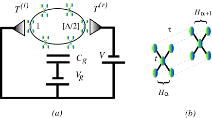
As in previous workPRB2003 , the central island consists in a ring of identical 5-site centered-square Hubbard clusters, denoted by the index , see Figs.1. Each cluster is described by the Hamiltonian
| (2) |
with the creation operators on the -th cluster for the central site, and , for the remaining 4 sites; , and is a spin index.
In the device, each cluster is linked to the two nearest neighbors ones (denoted by and ) by the hopping Hamiltonian (see Fig.1) whereby a particle in the -th site of the -th cluster can hop towards the -th site of the -th clusters:
| (3) |
also contains an electrostatic charging energy term due to an effective capacitance of the central island. Finally the island is connected capacitively to the gate which is at a potential (see Fig.1). Therefore we have
| (4) |
where is total number of particles operator in the central device. We remark that the capacitive term is essentially long-ranged and accounts for the monopole contribution to the charging energy, while the terms depend on the way the charges are distributed in the island. In all electrostatic terms should be referred to an average population corresponding to a neutral situation; but, actually, any shift would produce a constant and a linear term in that just modifies .
Both leads are free electron gases with chemical potentials , ; hence
| (5) |
with nota where is the bias.
Finally the tunneling Hamiltonian is taken to be
| (6) | |||||
where the are eigen-operators of the noninteracting term of : . We observe that the tunnel junctions connect two opposite clusters to the leads; namely the cluster is linked to the left electrode and the cluster to the right lead (here means the integer part of ), see Fig.1. Note also that is independent of , in other terms we are using ”white” wires, that is, leads that do not filter electrons according to the square symmetry of electronic states in each cluster. This is a simple way to ensure the 3D nature of the leads, which is essential to allow Andreev reflection.
In the next Section we draw some relevant properties of which mimic the behavior of despite the presence of strong electronic correlations.
III Properties of the Central Island
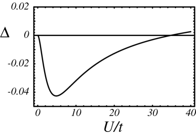
In order to understand the physics of the device that we propose, it is useful to foucus first on properties of , referred to a single 5-site cluster. The Hamiltonian is a prototype example of electronic pairing from repulsion; this is signaled by the property , where and is the ground state energy with electrons. There is pairing at for , the minimum value is meV at eV and eV and the binding energy is (see Fig.2). The mechanism has been investigated elsewherePRB1997 EPJB1999 , and need not concern us here; we just say that broadly speaking it is a lattice counterpart of the Kohn-Luttinger mechanismkohn .
When a negative occurs, its competition with determines the parity of the number of electrons in the ground state of for small values of the inter-cluster hopping .
Here we are interested in the behavior of the device at low temperatures Up to and corrections, the ground state energy of the central device with fixed even or odd number of particles is
| (7) |
where . Since one bound pair exists at electrons in the 5-site cluster, the first bound pair in the -cluster system appears at electrons. From Eq.(7), it follows that in the range is always even if the pair binding energy overcomes the charging energy. We call the situation when the superconducting regime. Otherwise the system is normal and any is lowest in a range of .
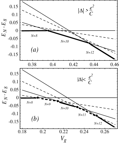
In Fig.3 we plot the ground state energy of as a function of in both regimes, for . It also relevant to focus on the critical values of where ground states of different cross. We define the spacing between the critical values in the normal regime and such a spacing in the superconducting regime; it holds
| (8) |
The charge fluctuations in the superconducting regime as a function of the gate voltage are about double spaced with respect to the normal regime, that is the typical condition experimentally realized in a S-SETdevoret .
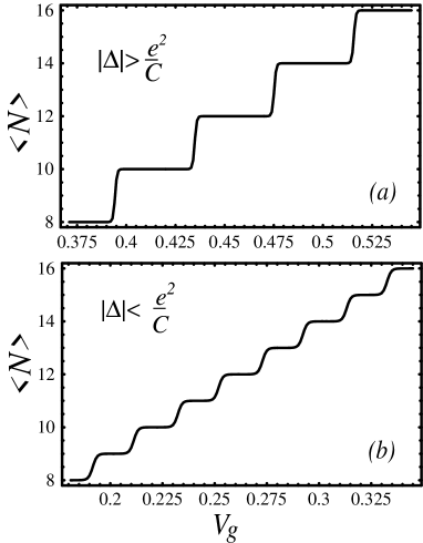
We can also visualize the previous results by plotting the gran-canonical average of the number of particles in the isolated central device as function of . We use the standard definition
| (9) |
where ; is dominated by the low energy states of with . In Fig.4 one can observe the so called Cooper staircase, characteristic of the superconducting regime.
Below, for computational convenience, we assume and deal with perturbativelyPRB2003 . So, the critical values of where level crossing occur, are spread into intervals of width in the normal regime and in the superconducting regime. Anyway the qualitative behavior is still close to Figs.3,4.
IV Calculation of the Linear Conductance
Next, we consider the effects of small bias voltage applied between leads, i.e. the linear conductance for , versus the gate voltage . In the present article, we follow the approach proposed by Beenakkerbeenakker and get the formula for the conductance from a master equation. We take in order to provide that the parity of the ground state is stable with respect to thermal effects, the elementary tunnel processes between the leads and the central devices involve few particles at a time and the broadening of the levels of due to the presence of the leads is smaller than the thermal one. As discussed by Beenakkerbeenakker , these limitations characterize the Coulomb blockade regime.
In the normal regime single-electron tunneling dominates. The theory works very much like in Ref.beenakker and we calculate the first-order transmission rates
| (10) |
from the -th state of the central device with particles (denoted ) to the -th state of the central device with particles ( ) via tunneling to the left () or rigth () lead. Remember that for and for . In the actual calculations below, we obtain in second-order perturbation theory in ; we mix the degenerate ground-state multiplets of energy of , which determine the low-energy properties of the system. By first-order perturbation theory in , one gets the familiar formula:
| (11) | |||||
Here, is the Boltzmann equilibrium probability for occupying the eigenstate with energy ; is the Fermi distribution function, and is the density of states at the Fermi level in both leads. Each term in Eq.(11) depends on through the statistical factor and produces the well known Coulomb blockade behaviorbeenakker zhiming . The linear conductance is highly suppressed unless the gate voltage is fine tuned at , where sharp peaks of occur. The second-order contribution in depends on rates which are negligible with respect to the coefficients; therefore we can safely avoid working out the second-order current in this regime.
When , only even have an important weight in the appropriate range of (see Fig.3 ); therefore the resonance condition never holds and the first-order conductance is highly suppressed for any value of . In this pair tunneling regime, accordingly, we must go on calculating the conductance up to second-order in averin hekking hanke . Three-body, four-body transitions and so on can be disregarded, however, as and are both small compared to the charging energy. Since electrons can get paired in the device but not in the leads, we may think of the second-order processes in terms of Andreev reflections. First one of the two electrons tunnels from one lead to the device (which is in the state) and forms a virtual excited state. Then the second one tunnels into the device and form a bound pair ( state).
In principle in second-order, one should also take into account the cotunneling processesaverin2 , which leave the population of the central island unchanged. Such processes provide a current away from the resonances. Anyway, as long as our device is in small bias and low temperature regime, the cotunneling current is found to be negligible, as in the case of Ref.hekking . Therefore the sequential tunneling is the major transport mechanism, and it is possible only at the two-electron degeneracy points.
The full derivation of the solution of the detailed balance equationsbeenakker will be presented elsewhere. Setting
| (12) |
one gets for the conductance
| (13) |
The amplitude
takes into account the second-order process governing the Andreev reflection. Eq.(IV) predicts Coulomb blockade peaks for every such that , while the conductance is strongly suppressed elsewhere. Each peak has a correlation weight due to the coefficient , containing all the microscopic information on the correlated ground states of the central device.
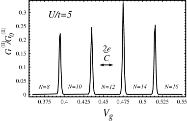
For illustration, we numerically computed the conductance for a central device with In the superconducting regime, as a function of the gate voltage is shown in Fig.5 for eV, eV, eV, eV, e/. Note that eV, and eV. shows neat peaks, with spacing V.
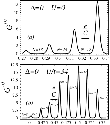
This superconductor-like behavior depends on the existence of pairing. As a countercheck, we calculate the linear conductance in the normal regime, when . We can obtain this condition in two ways, namely in the non-interacting case when and in the very strongly correlated regime, when eV, the other parameters remaining the same as in Fig.5. is plotted in Fig.6; since we are mainly interested in the period of the resonances, we use constant ’s and plot the results in arbitrary units. Indeed, for the period of the resonant peaks is V, i.e. a half of the period in the superconducting case.
V Summary and Conclusions
We have shown that the Hamiltonian models a S-SET in the linear regime. We pointed out that the repulsion-induced pairing occurring in fixes a characteristic energy which competes with the electrostatic charging energy . As in any S-SET, there is a normal regime, where and a superconducting regime, where . In the first case the parity of the electron number in the ground state oscillates between even and odd values and the transport properties are governed by single-electron tunneling. Conversely in the superconducting regime the parity is always even and the major transport mechanism is sequential tunneling of pairs. The explicit calculations have been performed for a ring of four 5-site clusters, but a general expression for the linear conductance is also derived.
Our results suggest a systematic way to produce a well controlled periodic two-electron pattern, even without any conventional superconductivity; an array of quantum dots similar to the one in Ref. ashoori could be designed to this purpose.
Finally we underline that the model we propose is very flexible with respect to the size and the shape of the Hubbard clusters, to the topology of the cluster array forming the central device. Indeed a wide variety of Hubbard clusters show the property at proper fillings, which is actually the key feature at the basis of our device; we could construct many alternative devices, based on graphs with different topologies, also in view of possible single-electronics applications to more complex circuits than a transistor.
References
- (1) See for example A.A.Aligia, K.Halberg, B. Normand and A.P. Kampf, Phys. Rev. Lett 93, 076801-1 (2004) and references therein.
- (2) M. A. Kastner, Rev. Mod. Phys 64, 849 (1992).
- (3) In this case the device is usually denoted by NSN-SET, in order to distinguish it from SSS-SET, where the superconducting island is connected to superconducting leads; anyway in this article we use S-SET for short.
- (4) T. M. Eiles, J. M. Martinis, and M. H. Devoret, Phys. Rev. Lett 70, 1862 (1993).
- (5) D. V. Averin, and Yu. V. Nazarov, Phys. Rev. Lett 69, 1993 (1992).
- (6) F. W. J. Hekking, L. I. Glazman, K.A. Matveev, and R. I. Shekhter, Phys. Rev. Lett 70, 4138 (1993).
- (7) U. Hanke, Y. Galperin, K. A. Chao, M. Gisselfält, M. Jonson, and R. I. Shekhter, Phys. Rev. B 51, 9084 (1995).
- (8) R.C. Ashoori, H.L. Stormer,J.C. Weiner, L.N. Pfeiffer, S.J. Pearton, K.W. Baldwin, and K.W. West, Phys. Rev. Lett 68, 3088 (1992).
- (9) M.E. Raikh, L.I. Glazman, and Zhukov, Phys. Rev. Lett 77, 1354 (1996).
- (10) C.M. Canali, Phys. Rev. Lett 84, 3934 (2000).
- (11) C. W. J. Beenakker, Phys. Rev. B 44, 1646 (1991).
- (12) Agnese Callegari, Michele Cini, Enrico Perfetto and Gianluca Stefanucci, Eur. Phys. J. B 34, 455, (2003); Phys. Rev. B 68, 153103, (2003).
- (13) M. Cini and A. Balzarotti, Phys. Rev. B 56, 14711 (1997).
- (14) Michele Cini, Gianluca Stefanucci and Adalberto Balzarotti, Eur. Phys. J. B10, 293 (1999).
- (15) W. Kohn and J. M. Luttinger, Phys. Rev. Lett. 15, 524 (1965).
- (16) With reference to Eq.(1), the total number of particles is .
- (17) Zhiming Yu, Thomas Heinzel, and A. T. Johnson, Phys. Rev. B 55, 13697, (1997).
- (18) D. V. Averin, and Yu. V. Nazarov Phys. Rev. Lett 65, 2446 (1990)