Metallic behaviour of carrier-polarized C60 molecular layers: Experiment and Theory
Abstract
Although C60 is a molecular crystal with a bandgap of eV, we show that is strongly affected by injected charge. In sharp contrast to the Coulomb blockade typical of quantum dots, is reduced by the Coulomb effects. The conductance of a thin C60 layer sandwiched between metal (Al, Ag, Au, Mg and Pt) contacts is investigated. Excellent Ohmic conductance is observed for Al electrodes protected with ultra-thin LiF layers. First-principles calculations, Hubbard models etc., show that the energy gap of C60 is dramatically reduced when electrons hop from C to C60.
pacs:
PACS Numbers: 05.30.Fk, 71.10.+x, 71.45.GmThe Fullerene C60 solid is a molecular crystalsawatsky with a bandgap of eV. Alkali-metal doping makes it a conductor or a superconductorgunnerson . Other methods of converting C60 into a conductor involve exotic chemical routes where, e.g., C60 molecules are joined by metal-ligand structuresjacs . Such efforts focus on improving the conductance of the molecular layer itself. Another important factor is the electrical contact between the molecular layer and the metal surface. The practical realization of molecular electronics depends crucially on this molecule/metal contact. In many situations, such contacts involve chemical processes that lead to fragmentation of the molecules themselvescritique ; turak .
Fullerenes, e.g., C60 are popular candidates for molecular electronics. Unlike quantum dots and related nanostructures, molecules come in identical copies and have energy levels which are robust at room temperature. Many studies on moleculer-C60 devices have emphasized negative-differential resistance (NDR)ndr , or the control of conductance using scanning-tunnelling probes, electromechanical and other gatesguo . In the simulation by Taylor et alguo , a single C60 molecule is positioned between two Al leads. In their ideal device, metallic conductance occurs when the triad of degenerate LUMO (lowest-unoccupied molecular orbital) acquires three electrons forming a half-filled band. Hubbard-like effects are assumed negligible in their calculations; the LUMO is 1.8 eV above the HOMO (highest occupied molecular orbital) in the local-density approximation (LDA).
Given that single-molecule current () and voltage () data are still controversialcritique , we turn to the the data for C60 films sandwiched between two metal electrodes. Usually the top electrode is formed by depositing hot metal onto the organic film already deposited on a cold, crystallographically uncontrolled metal surface.
Studies of C60 layers deposited on crystallographically controlled surfaces of Al, Ag, Au, Mg, etc.c60al ; auag , show that charge transfer, electronic and bonding modifications occur within the first monolayer of molecules, but the second monolayer usually remains unaffectedauc60layer1 ; agbell , except for weaker physical effects. More than one C60 monolayer may be affected if the surface is polycrystalline. We call this physico-chemically modified interface-layer the metal-fulleride layer. The metal-fulleride formation for C60 deposition on Al, as well as for Al deposition on C60 has been studied by, e.g., Owens et al.c60al . The interaction is more complex than resulting from image-charge effects or simple charge transfer, as may perhaps be the case for Ag. The situation is even more complicated for Pt and Ni surfaces which form strong bonds with C60 and catalyse the decomposition of the organic molecule at sufficiently elevated temperaturesPtNi . If the “bulk” C60 material is clean and undoped, very few carriers are available for producing “band-bending” effects of dipole layers etc., as found at doped inorganic semi-conductor interfaces. This implies that, except for the fulleride layer next to the electrode, the molecules in the “bulk” are unaffected by the presence of the metal contacts. This picture assumes that hot-metal atoms were not bombarded into the organic filmc60al ; agbell , or that the metal was not presented as a paste or other preparation where metal diffusion into the C60 could occurohmic1 .
Most reportskatz ; sarici of behaviour on such metal/C60/metal sandwich structures suggest semiconducting, rectifying or insulating behaviour. In a previous paperapl1 we showed how an ultra-thin layer of LiF dramatically modifies the characteristics of a molecular film by (i) protecting the organic molecules from reactions with the metal, (ii) creating a sharp electrode density of states (DOS) and favouring carrier injection. Similar important effects of ionic epilayers on metals are not uncommonag_mgo . Here we study C60 molecular films and show that the charge injection dramatically changes the “insulating” or semi-conducting character of C60 films. Metallic conductance is achieved for M = Al and Mg. That is, the current depends linearly on the applied bias , for both forward and reverse bias. When M=Pt, the conductance is very small, non-linear and there is strong asymmetry on reversing the bias. We note that the work functions for polycrystalline Mg, Ag, Al, Au and Pt are 3.7, 4.3, 4.3, 5.1 and 5.7 eV respectivelyworkfunc . Although there is some correlation with the work function, the situation is more complex since carrier hopping is subject to Coulomb interactions as well.
Even if the C60 monolayer (fulleride layer) just next to the metal electrode acquires electrons due to interactions with the metalagbell , conduction cannot occur unless there is a mechanism for further charge transfer from molecule to moleculehopping in undoped C60. We clarify the observed metallic behaviour using detailed electronic structure calculations. The energy gap of the “bulk” C60 molecules dynamically collapses as the carrier electrons hop from molecule to molecule. That is, an inverse Coulomb blockade occurs, where charge transfer between the highly polarizable C60 molecule is enhanced. In metals like Pt where fulleride formation via metal -orbitals is likely, charge injection is negligible under low bias; here strongly non-linear is observed. Thus while neutral C60 behaves as a molecular crystal in photoemission experimentssawatsky , our experiments and calculations suggest that C60 may behave as a metal in the presence of polarizing carriers.
Experimental.– Details of sample fabrication etc., are given in Lu et al.apl1 . The devices were made on 2 in2 in Si(100) wafers with 2000 nm furnace oxides on top. The first metal (Al, Mg, Ag, Au, Pt) electrode (1 mm wide, 50 mm long, and 60 nm thick) was deposited through a shadow mask, and is referred to as the “bottom” electrode. C60 films (210 nm thick) were then deposited over the bottom electrode. A second metal (Al) electrode (1 mm wide, 50mm long and 100 nm thick), referred to as the “top electrode”, was deposited over the C60 films. An ultra-thin layer ( 1 nm) of LiF was deposited on the C60 film prior to the deposition of the top electrode. The top electrode lines were orthogonal to the bottom electrode lines so that each intersection of these two lines produces one metal/C60/metal device. There are 20 to 100 devices on each wafer. A final silicon oxide film of 300 nm was used to encapsulate the device. This final encapsulation is essential to produce consistent and reproducible results. Such protection is important since contamination with air has a drastic effectair on the electrical properties of C60. All devices were made using a K.J. Lesker 4 in x 4 in Cluster Tool having several process chambers inter-linked through a central distribution chamber. All metals were deposited in the metallization chamber having a base pressure of 10-7 Torr. The C60 molecules were deposited in the organic chamber having a base pressure of Torr. The transfer of samples between chambers was via a central chamber, with a base pressure of Torr. The measurements were in a dark, ambient environment, using an HP4140B meter with a Materials Development probe station.
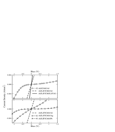
Figure. 1, top panel shows the data for samples which differ in the presence or absence of LiF interlayers. In samples with bare-Al electrodes , i.e., Al//C60//Al the left-hand Al (the “top” electrode) was deposited hot on C60, while the right-hand Al electrode (“bottom” electrode) was cold during C60 deposition. In such systems the fulleride interlayers are uncontrolled and they are denoted by, //, a double bar. In devices with LiF at the top electrode, i.e, Al/LiF/C60//Al, the C60 is protected from the hot deposition of the “top” Al electrode.
The device with bare Al electrodes produces a typical diode-like behaviour (see Fig. 1, top panel) with negligible current flow at low bias. The reverse-bias current flow “takes off” more rapidly, as seen in the figure. The use of a LiF interlayer at the top electrode (the “hot-deposited” electrode) is enough to create a linear relationship with zero threshold for current flow. This is typical of metallic conductors. When a LiF interlayer is included at the bottom electrode as well, the conductance () improves only slightly, showing that the bottom electrode, where C60 was deposited in the cold, required no LiF protection. The behaviour is completely metallic, with no discontinuity in the gradient on changing the sign of . This was confirmed for C60 layer varying from 100 nm to 250 nm in thickness. It is clear that Al3+ migration into the C60 layer cannot be the cause of the conductance (as was the case in Ref. ohmic1 ), since such migration is obstructed by the LiF layer. Photoemission experiments suggest that only the first few monolayers of C60 near the metal are affected by the presence of the metalauag . The data show that fulleride formation at the cold-deposited C60 on the Al interface is not critical to electron transport, while the prevention of fulleride formation at the hot-deposited Al on C60 is absolutely important. The improved conductance of the sample with the Al electrodes protected with LiF confirms the protective role of LiF. This also suggests that the resistance of the device is determined by that of the fullaride layer which plays the role of the least conducting link.
Figure 1, bottom panel shows typical results for Al, Ag and Pt. Both Al and Mg (not shown) show metallic behaviour. However, surprisingly, Ag shows some slight non-linearity in its , revealing some interface reactivityauag . Results for Au (not shown) tend to be significantly more non-linear than for Ag. The Pt/C60 interface is clearly very unfavourable for Ohmic .
Theory.– We have studied the HOMO-LUMO energy gap as well as the electronic density of states (DOS) for the C60 molecule, for CLiF, CC60, CC and CC structures, where the short bar stands for all the interactions between the two moities. These electronic-structure details are obtained from density functional calculations using the Gaussian-98 codeG98 at the BP86/6-31G* levelacro ; G98 . The calculations included geometry optimization via total energy minimization using gradient corrected exchange-correlation functionals. The modifications in the DOS of some of the C60 structures are shown in Fig. 2, and in table I. In the upper panel we compare our isolated-molecule DOS with the experimental resultsauag for multilayers of C60 on Ag obtained using direct and inverse photoemission (UPS and IPS). Thus the HOMO part of the experimental curve is from UPS (energy resolution eV), and the LUMO part of the curve is from IPS (energy resolution eV). We have positioned these experimental curves so that our calculated HOMO (H) and LUMO (L) peaks align with the experimental H and L peaks. The general agreement clearly confirms that the molecules in a C60 multilayer deposited on Ag are essentially like isolated molecules. This also serves to confirm the validity of our theoretical calculations.
The presence of LiF itself produces a decrease in the C60 energy gap. Here the distance between the LiF and the C60 center, as well as other inter-nuclear distances have been energy optimized, and hence this is the upper-bound to the gap reduction that may arise from LiF.
The energetics of the C60 interactions is given in Table LABEL:energies. The energy gaps given in the Table improve on the gaps calculated using the local-density approximation (LDA). Thus the LDA gap for C60 is only eV, and differs from the experimental solid-state gap of eV. Our spin density-functional calculations show a spin-polarized energy-level structure for the anion. The electrons of the C60 system form a low-density quasi-2D electron fluid. Such systems have spin dependent ground states under suitable conditionspd2d . This may be of importance in spin transport applications using suitable C60 based systemspasupathy , although here the spin splitting is only about eV.
| system | a.u. | a.u. | eV. |
|---|---|---|---|
| C60 | -0.22003 | -0.11854 | 2.8 |
| CLiF | -0.18993 | -0.16157 | 0.8 |
| CC | -0.11880 | -0.06443 | 1.48 |
| CC | -0.11736 | -0.06213 | 1.50 |
| CC | -0.28683 | -0.23093 | 1.52 |
| CC | -0.28485 | -0.22942 | 1.51 |
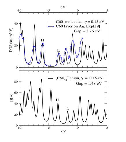
Photoemission experimentsc60al ; auag clearly establish the metallization of the first layer on metals like Ag and Al, with as much as 1.8 electrons transferredsawat4 to the LUMO in the case of Ag. That this is close to 2 electrons per molecule suggests that the Hubbard like on-site repulsion has been reduced from that of the isolated molecule. An electron transferred to a C60 molecule, and subject to the applied bias, hops to an adjacent C60 when carrier transport occurs. The final state of such a hop is given in our calculations for the (CC60)- anion, and shows a reduced gap. This is due to (a) splitting of the five-fold HOMO and the three-fold LUMO multiplets by the electric field of the in-coming charge, (b) polarization and distortion of the of the molecules which persist under stationary state conditions, (c) resulting modification of the on-site Coulomb interactions. Many of these issues have been examined using Hubbard type modelssawatPol , or with microscopic approaches. Hesper et al.hesper used an image-charge model for C60 on Ag to obtain a gap reduction of eV. They even mention the possibility of ”driving the insulator into the metallic state”. Our explicite calculations (Table I) can be used to parametrize the Hubbard models. However, even the Hubbard-model conductance has not been evaluated, except in special cases (e.g, infinite-dimensional Hubbard models).
In the usual picture of electron transport across molecular devices like: A/Molecular-layer/B, it is assumed that an electron is injected from the source electrode A into the LUMO of the nearest molecule, converting it to a transient, excited anion. This involves Coulomb blockade, rearrangement of bond lengths, bond angles etc., to give the actual anion. At this point the carrier may become localized on the molecular site as a poloron. Then no conduction occurs until a suitably high bias is applied. Or, if the energy offsets are favourable, the carriers may hop to neighbouring molecules and successively move towards the drain electrode. In the devices discussed here, the fulleride layers for Al, Mg and Ag are already populated at the LUMO with up to 1.8 electrons. Thus the 1st layer of C60, i.e., the metal-fulleride layer contains charge which polarizes the second layer and enables the hopping of electrons under the applied bias. The usual van der Waals crystal now behaves as a conductor. The conductance is determined by the weakest factor, viz., the transmission coefficient for the process, metal-fulleride C60 bulk-like layer. An evaluation of is postponed till a detailed fulleride-C60 calculation becomes available.
Our geometry optimizied calculations (Table I) includes the electron-phonon interaction to all orders. The importance of these effects is recognized, especially within the alkali-doped fullerides like K4C60 which is an insulator due to bond-distortion effects. Also, K6C60 is a band insulator since the 6 electrons per molecule completely fill the three-fold LUMO. In our system, the LUMO of the fulleride layer is only occupied to 1.8 electronssawat4 per C60 molecule.
In conclusion, we have shown, experimentally and theoretically, that characteristics similar to a metal can be obtained using LiF protected low-workfunction electrodes connected to C60 layers.
acknowledgements- We thank George Sawatzky (UBC) for his valuable comments.
References
- (1) R. W. Lof et al, Phys. Rev. Lett. 68, 3924 (1992)
- (2) O. Gunnerson, Rev. Mod. Phys. 69, 575 (1997)
- (3) Kwanggyeao Lee et al, J. Am. Chem. Soc. 124, 2873 (2002)
- (4) see R. F. Service, Science, 302, 556 (2003)
- (5) A. Turak et al., Appl. Phys. Lett. 81, 766 (2002).
- (6) C. Zeng et al, Appl. Phys. Lett. 77, 3595 (2000)
- (7) J. Taylor et al, Phys. Rev. B 61 121104 (2001)
- (8) D. W. Owens et al., Phys. Rev B 51 17068 (1995)
- (9) D. Purdie et al., Surface Science, 364, 279 (1996)
- (10) A. J. Maxwell et al., Phys. Rev. B 49,10717 (1994).
- (11) G. K. Wertheim et al, Phys. Rev. B 50, 11070 (1994)
- (12) C. Cepek et al, Phys. Rev. B 53, 7466 (1996)
- (13) L. Firlej et al, Phys. Rev. B 59, 16028 (1999)
- (14) A. Hamed, Phys. Rev. B 47, 10873 (1992)
- (15) E. A. Katz et al, Electronic Properties of Novel materials: XII, AIP, pp 527 (1998)
- (16) N. S. Sariciftici et al, Appl. Phys. Lett. 62, 585 (1993)
- (17) Z. H. Lu, R. S. Khangura, M. W. C. Dharma-wardana, M. Z. Zgierski, and D. Ritchie, App. Phys. Lett. 85, 325, (2004)
- (18) S. Altieri et al., Phys. Rev. B 59, R2517 (1999). M. Kiguchi et al., Phys. Rev. Lett, 90, 196803 (2003).
- (19) H. B. Michaelson, J. Appl. Phys. 48, 4729 (1977)
- (20) P. A. Brŭhwiler et al., Phys. Rev. Lett. 71, 3721 (1993); 73 2938 (1994) and M. B. J. Meinders et al., 73, 2937 (1994)
- (21) Gaussian 98, Revision A.9, M. J. Frisch et al, Gaussian Inc., Pittsburgh, PA (1998).
- (22) For the acronyms, basis sets, etc., see: A.D. Becke, J. Chem. Phys., 98, 5648 (1993); C. Lee, W. Yang and R.G. Parr, Phys. Rev. B, 37,785 (1988).
- (23) M. W. C. Dharma-wardana and F. Perrot, Phys. Rev. Lett. 90, 136601 (2003)
- (24) A. N. Pasupathy et al., Science 306, 86 (2004)
- (25) J. van den Brink et al., Phys. Rev. Lett. 75, 4658 (1995)
- (26) R. Hesper et al., Europhys. Lett., 40, 177 (1997)
- (27) B. W. Hoogenboom et al., Phys. Rev. Lett. 57, 11939 (1998)