Kondo Effect in Electromigrated Gold Break Junctions
Abstract
We present gate-dependent transport measurements of Kondo impurities in bare gold break junctions, generated with high yield using an electromigration process that is actively controlled. Thirty percent of measured devices show zero-bias conductance peaks. Temperature dependence suggests Kondo temperatures . The peak splitting in magnetic field is consistent with theoretical predictions for g=2, though in many devices the splitting is offset from by a fixed energy. The Kondo resonances observed here may be due to atomic-scale metallic grains formed during electromigration.
The physics of many-particle entangled spin states has attracted recent interest in a variety of systems. The correlation that may form at low temperature between a localized electron spin and a surrounding Fermi sea is one of the most carefully studied of these states. This correlation gives rise to the Kondo effect, originally observed in the 1930’s as an enhanced low-temperature resistance in magnetically-doped metalsMeissner and Voigt (1930). Several decades later a new manifestation of the same physics was discovered in systems where a charge trap is positioned between two electrical leadsAppelbaum (1967); Shen and Rowell (1968); Bermon et al. (1978); Gregory (1992); Ralph and Buhrman (1994).
During transport, electrons tunnel from one lead onto the trap and off to the other lead. In general, transport is allowed only when two charge states are degenerate, an effect known as Coulomb blockade. If the trap binds an unpaired electron, high-order tunneling processes may give rise to an enhanced conductance at zero-bias in spite of Coulomb blockade. Metal tunnel junctions containing paramagnetic impurities were the first systems to show the narrow zero-bias peak characteristic of this effectAppelbaum (1967); Shen and Rowell (1968); Bermon et al. (1978); Gregory (1992); Ralph and Buhrman (1994). The peak splits in magnetic field, and is suppressed above the Kondo temperature, .
The Kondo temperature corresponds to the energy of formation of the many-body spin state; it depends exponentially on the binding energy of the trap, , and the coupling to the leads, : Ralph and Buhrman (1994). An electrostatic gate can be used to control by tuning , and can even turn off the Kondo resonance by changing the number of bound electrons. A gateable Kondo effect was first observed in lithographically-defined quantum dotsGoldhaber-Gordon et al. (1998a); Cronenwett et al. (1998), where the primary difficulty was achieving a Kondo temperature high enough to be experimentally accessible.
Larger Kondo temperatures can be found in much smaller systems consisting of an atomic-scale charge trap between two metallic leads. However, fabrication of such leads in a gateable geometry is a formidable lithographic challenge. One successful approach is to break a single wire into an electrode pair using electromigrationPark et al. (1999), the process by which an electric current causes the atoms in a conductor to moveHo and Kwok (1989). Both Coulomb blockade and the Kondo effect have been observed in electromigrated gold junctions with organic molecules deposited on the surface as charge trapsPark et al. (2002); Liang et al. (2002); Yu and Natelson (2004a).
In this Letter we show that localized states giving rise to the Kondo effect may be found even in the gated gold junction itself. Active control over the electromigration process gives a high yield (up to ) of devices showing zero-bias peaks that are suppressed at finite temperature and split with magnetic field. For most devices, fell in the range . Above the splitting was linear in field with slope g=2, but the absolute magnitude of the splitting varied from device to device for reasons that are not yet understood. We discuss possible sources of the Kondo resonance in bare junctions, focusing on atomic-scale metallic grains. Grains consisting of atoms, formed in electromigrated junctions, have been shown to possess novel optical propertiesGonzalez et al. (2004); the transport properties presented here offer a further glimpse of the rich physics in this system.
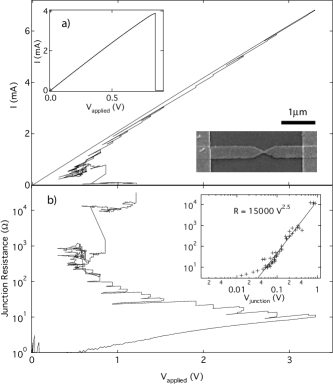
The devices (Fig. 1a inset) are patterned on a GaAs substrate using a combination of optical and electron beam lithography and a resist/liftoff process. A thick aluminum back gate is deposited by evaporation with the substrate held at . The surface is oxidized for ten minutes in ozone under a UV lamp. Gold wires ( thick) are deposited on the gate at room temperature; each tapers to a constriction. A gold layer connects the narrow wires to optical lithography. The pressure during evaporation was . The devices are cleaned with acetone and methanol, followed by oxygen plasma to remove any residual organic materials. Electromigration is performed in a refrigerator containing of exchange gas. The sample is then cooled immediately and measured.
An active control algorithm differentiates the electromigration performed here from previous work. When junctions are created without using feedback, the yield showing even weak tunneling is low () and there is little control over final resistance. For better control we monitor the resistance of the entire electromigration circuit and adjust the voltage to maintain a constant break rate, measured as , where is the resistance of the circuit after subtracting a lead resistance. Break rate is extracted from resistance measurements at fixed voltage, taken over .
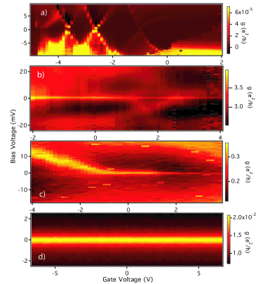
Figure 1 shows the two stages of a typical break. In the first (A to B), the break rate is negligible as the voltage is ramped up. Once the break rate exceeds a target (), the voltage is actively adjusted to maintain that rate (B to C). When the resistance exceeds , the voltage is reduced to zero at . There is remarkable consistency from device to device; extracted power laws indicate that constant power is dissipated in the break region for the B-C stage (see Fig. 1b inset).
We present results for electromigration of wires, of which broke to a room-temperature resistance between and . We cooled of these to and measured differential conductance as a function of gate voltage and DC biaswhy . No conductance, or only weakly nonlinear conductance, was visible in devices. Three showed a gate-independent conductance dip at zero bias suggesting transport through metallic grains in good contact with the leadsAnaya et al. (2003).
The remaining 38 showed transport through charge traps: Coulomb blockade or a Kondo resonance (see Fig. 2). The binding energy of these traps is primarily determined by the energy, , needed to add or remove an electron from a trap. No device that showed a Kondo resonance also showed two charge degeneracy points, necessary for accurate measurement of ; in many the conductance was featureless up to hundreds of . However, multiple Coulomb diamonds were occasionally observed in devices without Kondo resonances, giving values as low as in these (e.g. Fig. 2a).
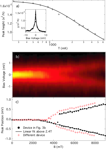
A zero-bias conductance peak was observed in devices. One signature of the Kondo effect is a suppression of the peak conductance with temperature: , where s = 0.22 for spin-1/2 impuritiesCosti et al. (1994); Goldhaber-Gordon et al. (1998b). We measured temperature dependence in peaks; all showed a good fit to this functional form, see e.g. Fig. 3a. The possibility of conductance pathways in parallel with the Kondo resonance (Fig. 2b) prevents reliable determination of from temperature dependence alone, so the width of the zero bias peak was used as confirmation. In most devices the peak width (defined as full width half maximum) was cos . We consider to be well-determined only in these devices. For most, ; none showed , and only one .
Gate dependence of the Kondo resonance was evident in of the devices, but charge degeneracy points, identifiable by a Coulomb diamond and representing a change in the number of bound electrons, were accessible in only three. In one, the zero-bias peak appears on only one side of the degeneracy point in gate voltage, as expected (see Fig. 2c). In the other two devices, however, the zero-bias peaks continue through the edge of the diamonds (Fig. 2b), leading us to suspect two parallel but independent conduction pathways.
Another identifying characteristic of the Kondo effect is the splitting of the zero-bias peak by in magnetic fieldAppelbaum (1967). Field dependence was measured in devices, and this signature was observed in allexp . The splitting was visible only above a device-dependent critical field, . Where was well-determined, , consistent with theoretical predictionsCosti (2000).
Above the splitting was linear; typical data are shown in Fig. 3. In 8 devices the slope of the splitting was consistent with . The other four showed g-factors up to 4.5; these anomalously large values are not yet understood. In contrast, theoretical work predicts a suppression of the g factor, to between 1.3 and 1.7, for up to several times Moore and Wen (2000); cos .
The measurements in this paper cover the regime , where exact theoretical predictions for conductance have not been worked out. We find for the splitting of the zero bias peak a surprisingly simple functional form: , where is device dependent. Even devices with the same factor and Kondo temperature show different values for (see e. g. Fig. 3c). A negative value, , was observed in one device, reminiscent of a recent observation in GaAs quantum dotsKogan et al. (2004).
A structure that consists simply of two gold electrodes above an electrostatic gate would not be expected to show either Coulomb blockade or the Kondo effect. The system must also contain one or more charge traps. While there are many candidates for charge traps in an electromigrated junction, the trends observed here may identify this additional component. Changes in the details of the electromigration procedure dramatically affect the yield of devices with zero-bias peaks, suggesting a strong dependence on the morphology of the gold. However, the range of is surprisingly narrow given the inherent randomness of electromigration and the sensitivity of to microscopic device parametersRalph and Buhrman (1994).
Defects in the gate oxide are an unlikely candidate for the Kondo resonance here, though they have been shown to give rise to the Kondo effect in other systemsAppelbaum (1967); Shen and Rowell (1968); Bermon et al. (1978); Gregory (1992); Ralph and Buhrman (1994). Some devices were gate independent, suggesting that the Kondo impurities can be in a location screened by the gold leads. In addition, the location of defect sites relative to the leads would vary from device to device, giving a wide range of .
Atomic or molecular adsorbates on the surface of the goldYu and Natelson (2004b) are a more plausible, but still unlikely, source of Kondo impurities. The coupling between an adsorbed molecule and a lead would depend only weakly on junction geometry, consistent with our results. Oxygen has been cited as a source of Kondo impurities in metallic tunnel junctionsBermon and So (1978). This possibility, however, does not explain the observed sensitivity to electromigration parameters. In addition, we performed the same process on a small number of devices in ultra-high vacuum (with the walls of the vacuum chamber held at ) and found similar device characteristics.
Isolated metal grains created during electromigration are the final possible Kondo impurity that we consider. Coulomb blockade in grains of size has been studied extensivelyRalph et al. (1995), and observed occasionally in bare electromigrated junctionsYu and Natelson (2004a). However, even over a wide range of lead-grain couplingsana , no observation of the Kondo effect has been reported.
In principle a metal grain, if well-connected to the leads, could show a Kondo temperature as high as those reported here. However, even in the limit of nearly perfect lead-grain contact, one expects for a grain with quantum level spacing Glazman et al. (1999). A rough geometric argument for a grain of radius then gives Ralph et al. (1995); even a modest range of sizes would result in a large range of , in contrast with our observations. In addition, gold grains larger than a few would exhibit a factor much less than 2 due to spin-orbit interactionsPetta and Ralph (2001).
A more likely candidate for the Kondo impurity in these devices is an atomic-scale gold nanocluster of the type reported in Ref. Gonzalez et al. (2004). Those nanoclusters, formed during electromigration, contained atomsGonzalez et al. (2004); Lee et al. (2002). This narrow range of sizes could explain the Kondo temperatures observed here, and the formation of these structures would depend strongly on the electromigration procedure. Atomic-scale nanoclusters are in many ways more similar to molecules than to larger gold grains, and could display many of the physical effects expected in single-molecule transport. The electronic measurements of many-body spin correlations presented here, together with the recent demonstration of single photon generation in these nanoclustersGonzalez et al. (2004), show the promise that this system may hold for coherent electronics in the solid state.
Electromigrated gold junctions have been used by many groups to measure transport through single organic molecules. Control experiments on bare gold wires were used to distinguish between transport features due to the molecules and those native to the electrode system. The sensitivity of our results to the details of electromigration demonstrates the difficulty in interpreting these control experiments, as simply the presence of molecules deposited on the surface may change the morphology of the gold. This sensitivity can also be an advantage: we find that the yield of Kondo resonances in bare junctions can be dramatically reduced by briefly applying a large voltage () across the junctions at room temperature. This large voltage is a natural result of more common electromigration procedures.
In summary, we have observed the Kondo effect in bare electromigrated gold junctions. The mere presence of Kondo resonances in this system is surprising and warrants further study. Careful analysis of the splitting at magnetic fields comparable to the Kondo temperature reveals a simple but unexpected functional form. Experiments are underway to better understand this behavior. The electromigration procedure outlined in this paper can also be extended to superconducting materials, and offers an experimental platform to test emerging theoretical models of the interplay between the Kondo effect and superconductivity.
Acknowledgements: This work is funded by an HP-MIT alliance through the Quantum Science Research Group, AFOSR MURI Award no. F49620-03-1-0420, and the NSF Center for Bits and Atoms. The authors thank T. Costi, D. Davidovic, G. Fiete, L. Glazman, D. Goldhaber-Gordon, H. Heersche, W. Hoftstetter, M. Kastner, C. Marcus, J. Moore, D. Natelson, A. Pasupathy, D. Stewart and S. Williams for valuable discussions and advice. AAH acknowledges support from the Hertz Foundation. JAF acknowledges support through a Pappalardo Postdoctoral Fellowship.
References
- Meissner and Voigt (1930) W. Meissner and G. Voigt, Ann. Physik 7, 892 (1930).
- Appelbaum (1967) J. A. Appelbaum, Phys. Rev. 154, 633 (1967).
- Shen and Rowell (1968) L. Y. L. Shen and J. M. Rowell, Phys. Rev. 165, 566 (1968).
- Bermon et al. (1978) S. Bermon, D. E. Paraskevopoulos, and P. M. Tedrow, Phys. Rev. B 17, 2110 (1978).
- Gregory (1992) S. Gregory, Phys. Rev. Lett. 68, 2070 (1992).
- Ralph and Buhrman (1994) D. C. Ralph and R. A. Buhrman, Phys. Rev. Lett 72, 3401 (1994).
- Goldhaber-Gordon et al. (1998a) D. Goldhaber-Gordon, H. Shtrikman, D. Mahalu, D. Abusch-Magder, U. Meirav, and M. A. Kastner, Nature 391, 156 (1998a).
- Cronenwett et al. (1998) S. M. Cronenwett, T. H. Oosterkamp, and L. P. Kouwenhoven, Science 281, 540 (1998).
- Park et al. (1999) H. Park, A. K. L. Lim, J. Park, A. P. Alivisatos, and P. L. McEuen, Appl. Phys. Lett. 75, 301 (1999).
- Ho and Kwok (1989) P. S. Ho and T. Kwok, Rep. Prog. Phys. 52, 301 (1989).
- Park et al. (2002) J. Park, A. N. Pasupathy, J. I. Goldsmith, A. V. Soldatov, C. Chang, Y. Yaish, J. P. Sethna, H. D. Abru, D. C. Ralph, and P. L. McEuen, Nature 417, 722 (2002).
- Liang et al. (2002) W. Liang, M. P. Shores, M. Bockrath, J. R. Long, and H. Park, Nature 417, 725 (2002).
- Yu and Natelson (2004a) L. H. Yu and D. Natelson, Nano Lett. 4, 79 (2004a).
- Gonzalez et al. (2004) J. I. Gonzalez, T.-H. Lee, M. D. Barnes, Y. Antoku, and R. M. Dickson, Phys. Rev. Lett 93, 147402 (2004).
- (15) Devices not cooled were used to test breaking procedure.
- Anaya et al. (2003) A. Anaya, A. L. Korotkov, M. Bowman, J. Waddell, and D. Davidovic, J. Appl. Phys. 93, 3501 (2003).
- Costi et al. (1994) T. A. Costi, A. C. Hewson, and V. Zlatic, J. Phys. Cond. Matt. 6, 2519 (1994).
- Goldhaber-Gordon et al. (1998b) D. Goldhaber-Gordon, J. Gores, M. A. Kastner, H. Shtrikman, D. Mahalu, and U. Meirav, Phys. Rev. Lett. 81, 5225 (1998b).
- (19) T. A. Costi, condmat/0212651.
- (20) Field dependence in a total of 15 devices was measured, but two were too noisy to extract a reliable splitting and one had too high a Kondo temperature: .
- Costi (2000) T. A. Costi, Phys. Rev. Lett. 85, 1504 (2000).
- Moore and Wen (2000) J. E. Moore and X.-G. Wen, Phys. Rev. Lett. 85, 1722 (2000).
- Kogan et al. (2004) A. Kogan, S. Amasha, D. Goldhaber-Gordon, G. Granger, M. A. Kastner, and H. Shtrikman, Phys. Rev. Lett. 93, 166602 (2004).
- Yu and Natelson (2004b) L. H. Yu and D. Natelson, Nanotechnology 15, S517 (2004b).
- Bermon and So (1978) S. Bermon and C. K. So, Solid State Comm. 27, 723 (1978).
- Ralph et al. (1995) D. C. Ralph, C. T. Black, and M. Tinkham, Phys. Rev. Lett. 74, 3241 (1995).
- (27) A. Anaya and M. Bowman and D. Davidovic, cond-mat/0402054.
- Glazman et al. (1999) L. I. Glazman, F. W. J. Hekking, and A. I. Larkin, Phys. Rev. Lett 83, 1830 (1999).
- Petta and Ralph (2001) J. R. Petta and D. C. Ralph, Phys. Rev. Lett 87, 266801 (2001).
- Lee et al. (2002) T.-H. Lee, J. I. Gonzalez, and R. M. Dickson, Proc. Natl. Acad. Sci. USA 99, 10272 (2002).