Threshold Voltage Shift in Organic Field Effect Transistors by
Dipole-Monolayers on the Gate Insulator
Abstract
We demonstrate controllable shift of the threshold voltage and the turn-on voltage in pentacene thin film transistors and rubrene single crystal field effect transistors (FET) by the use of nine organosilanes with different functional groups. Prior to depositing the organic semiconductors, the organosilanes were applied to the SiO2 gate insulator from solution and form a self assembled monolayer (SAM). The observed shift of the transfer characteristics range from -2 to 50 V and can be related to the surface potential of the layer next to the transistor channel. Concomitantly the mobile charge carrier concentration at zero gate bias reaches up to /cm2. In the single crystal FETs the measured transfer characteristics are also shifted, while essentially maintaining the high quality of the subthreshold swing. The shift of the transfer characteristics is governed by the built-in electric field of the SAM and can be explained using a simple energy level diagram. In the thin film devices, the subthreshold region is broadened, indicating that the SAM creates additional trap states, whose density is estimated to be of order /cm2.
pacs:
73.61.Ph 73.20.At 68.55.Jk 68.37.Yz 68.37.PsI Introduction
Organic semiconducting materials are used to fabricate transistors with electronic properties comparable to a-Si:H Klauk et al. (2002)Kelley et al. (2003), a material often used for back panel circuits of active matrix displays. These comparable electronic characteristics together with the promising low-cost fabrication Moore (2002) makes organic materials attractive candidates for use in commercial products. However, to manufacture integrated circuits with organic transistors the precise control of all electrical properties is required. In addition to the charge carrier mobility, the threshold voltage () is an important parameter that needs to be controlled to ensure proper operation of the circuits. The threshold voltage can depend on the time a gate voltage has been applied (bias stress) Knipp et al. (2003)Salleo and Street (2003)Street et al. (2003)Northrup and Chabinyc (2003)Gomes et al. (2004), on the exposure of the device to light V lkel et al. (2002) or it can be shifted using a polarizable gate insulator Katz et al. (2002). Furthermore, a dependence on the work function of the gate electrode Li et al. (2002) and the thickness of the active layer material Schroeder et al. (2003) has been reported. As we will show in this article, the threshold voltage additionally depends strongly on the preparation of the surface on which the organic material is deposited.
We present an experimental method to systematically study the influence of the surface treatment of the gate insulator on the threshold voltage and other electrical properties of pentacene thin film transistors (TFTs) and rubrene single crystal FETs. Top contact pentacene TFTs were fabricated on heavily doped and oxidized silicon wafers. Prior to the pentacene deposition the silicon dioxide gate insulator was treated with solutions of a variety of organosilanes with different degrees of electron acceptance properties. The organosilanes form self assembled monolayers on the SiO2 gate insulator and can advantageously modify the electronic properties of thin film transistors Lin et al. (1997a)Salleo et al. (2002). The single crystal FETs were fabricated by placing freshly grown crystals onto prepatterned wafers covered with various SAMs. The SAMs have a built-in dipole field depending on the molecule’s functional group and modify the (mobile) charge carrier density. This SAM-induced modification of the charge carrier density in the transistor channel is similar to applying a gate voltage. Both, the threshold voltage and the turn-on voltage are governed by the built-in electric field of the SAM. Similar results for bottom contact transistors have been reported recently by Kobayashi et al. Kobayashi et al. (2004).
The transfer characteristics of the single crystal devices are shifted by a certain gate voltage depending on the SAM, while maintaining a steep subthreshold swing. The thin film devices however, show a pronounced broadening of the subthreshold region. From this broadening an increased trap density is extracted that can partly be explained by a poor film morphology as observed with X-Ray diffraction (XRD) and atomic force microscopy (AFM) measurements, and partly by additional trap states.
II Experimental
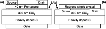
Figure 1 shows a schematic device cross section for thin film transistors (panel a) and single crystal FETs (panel b). Heavily doped silicon wafers with a 300 nm thick silicon dioxide insulating layer were used as substrates. The wafers were successively cleaned in hot acetone and hot isopropanol for three minutes in an ultrasonic bath, then with a piranha solution (70 vol% : 30 vol% ) for approx. 20 minutes, and were finally thoroughly rinsed in ultrapure water. The substrates were treated in a glove box with a relative humidity near 3 %. The treatment process was optimized for octadecyltrichlorosilane (OTS) and was applied in the same way for the other organosilanes.

To form the SAM, the wafers were immersed for 3 h in a 3 mM solution of the organosilane in anhydrous toluene McGovern et al. (1994). Fig. 2 shows the molecular structures of the studied organosilanes. After removing the samples from the solution they were cleaned in fresh toluene for 2 minutes in an ultrasonic bath to remove any excessive layers Tillman et al. (1988). We found this step to be crucial for good monolayer formation. The monolayers were then baked on a hot plate for 1 h at 150 ∘C Angst and Simmons (1991) in the same glove box to enhance cross-linking of the organosilane molecules and covalent bond formation to the silica surface.
To fabricate TFTs, the samples were transferred into the deposition chamber where pentacene was deposited at a rate of 0.3 0.1 Å/sec, by thermally evaporating pentacene powder that had previously been purified twice by temperature gradient vacuum sublimation. The nominal thickness of the organic layer was 40 nm and the base pressure of the system was near mbar. Unless otherwise noted, the substrate temperature during deposition was kept at 50 ∘C. In every deposition batch we deposited pentacene onto eight wafers at a time. Two of those wafers were treated with OTS to check the quality of the fabrication process and the rest were treated with three other organosilanes.
Gold source and drain contacts were deposited through shadow masks at a rate near 1 Å/sec. The channel width W was 600 m for all devices while the gate length L varied from 30 m to 150 m. With this configuration we could fabricate six transistors on every wafer. The electrical properties were measured with a HP 4155A semiconductor parameter analyzer, with the samples kept in an argon glove box ( ppm H2O, O2).
For the single crystal experiments, 20 nm thick gold source and drain contacts were evaporated after cleaning the wafers, forming bottom contacts. After finishing the treatment process, rubrene single crystals grown as described in Goldmann et al. (2004) were carefully placed on the prepatterned structures completing the transistors. The measurement procedure was the same as for the thin film transistors.
III Results and Discussion
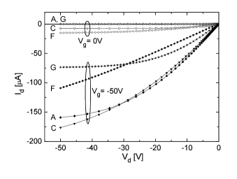
The output characteristics of TFTs with four different surface treatments are shown in Fig. 3. A non-zero drain current at zero gate bias is measured for transistors (C) and (F) while it is zero on a linear scale for the OTS treated transistor (A) and transistor (G). This indicates the presence of mobile charge carriers at zero gate bias. The drain current at negative gate bias saturates in transistors with treatments (A) and (G), following the standard MOSFET behavior Sze (1988). For transistor (C) this saturation is not as pronounced and for transistor (F) no saturation is observed, indicating a large positive threshold voltage (Vt) so that the device is still operating in the linear regime ().
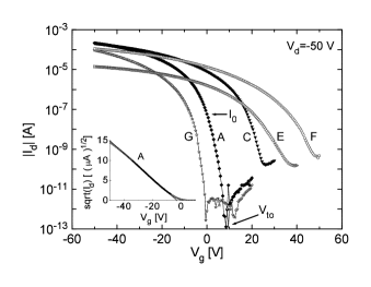
To illustrate the presence of mobile charge carriers at zero gate bias we show in Fig. 4 the transfer characteristics as log versus for the same transistors as in Fig. 3 and the transistor with treatment (E). The magnitude of the drain current at V shows a dependence on the SAM and is marked in Fig. 4 for the OTS (A) treated transistor. In addition to the increase of , an increased off-current is observed for treatments (C)(E) and (F).
To quantify the measurements we use the turn-on voltage , which is the gate voltage where the drain current starts to increase exponentially. For polymer devices a switch-on voltage was defined in a similar way Meijer et al. (2002) and marks the flat band condition. The turn-on voltage is marked in Fig. 4 for transistor (A). It is slightly positive for (A) V which is commonly observed for OTS treated devices, and it increases significantly for treatment (C) V, (E) V and (F) V. The only treatment with negative turn-on voltage is the phenyl treatment (G) V, meaning that the transistor is completely switched off at zero gate bias and the transistor is operating entirely as an enhancement mode device, which can be desirable for designing circuits.
| [∘] | [cm2/Vs] | [V] | [V] | [V/dec.] | [A] | |
|---|---|---|---|---|---|---|
| (A) Octadecyltrichlorosilane | 95 | |||||
| (B) Butyltrichlorosilane | 93 | |||||
| (C) 3-Chloropropyltrichlorosilane | 75 | |||||
| (D) 3-Bromopropyltrichlorosilane | 80 | |||||
| (E) Trichloro(3,3,3-trifluoropropyl)silane | 91 | |||||
| (F) 1H,1H,2H,2H-Perfluorooctyl-trichlorosilane | 105 | |||||
| (G) Phenethyltrichlorosilane | 92 | |||||
| (H) 4-(Chloromethyl)phenyltrichlorosilane | 88 | |||||
| (I) 2-(4-Chlorosulfonylphenyl)ethyltrichlorosilane | 90 |
Table 1 summarizes the results for , , , subthreshold swing S (for the 300 nm thick SiO2 gate insulator) and calculated mobility for the nine treatments, together with the water contact angle of the treated surface. The threshold voltage was defined as the intercept of a linear least square fit to versus as illustrated in the inset to Fig. 4. The range between 20% and 80% of was taken for this fit, and the mobility was calculated from the slope. The subthreshold swing was extracted from the logarithmic plot of the transfer characteristics shown in Fig. 4. The values in Tab. 1 represent the average values and the standard deviation measured on typically nine transistors fabricated on two different wafers in the same batch.
We will discuss two mechanisms possibly involved in the shift of the threshold voltage and the turn-on voltage: the influence of the film morphology and the effect of the built-in electric field of the SAM (”SAM-induced charge”).
III.1 Influence of the Film Morphology
| T [∘C] | [cm2/Vs] | [V] | [V] | [/cm2] | |
|---|---|---|---|---|---|
| 30 | 0.4(1) | -8(3) | 2(5) | 0.7(6) | |
| (A) | 50 | 0.9(1) | -4(1) | 4(2) | 0.6(2) |
| 70 | 1.3(2) | -10(2) | 0(3) | 0.7(4) | |
| 30 | 0.6(1) | -11(1) | -1(1) | 0.9(1) | |
| (B) | 50 | 0.7(1) | -4(0.5) | 5(2) | 0.6(2) |
| 70 | 0.9(1) | -11(1) | 0(0.5) | 0.8(1) | |
| 30 | 0.4(.05) | 24(6) | 45(8) | 1.5(1.0) | |
| (I) | 50 | 0.4(.05) | 25(3) | 48(2) | 1.6(4) |
| 70 | 0.3(.02) | 26(2) | 50(1) | 1.7(2) |
The film morphology has been shown to influence the charge carrier mobility Knipp et al. (2003)Lin et al. (1997a)Shtein et al. (2002)Gundlach et al. (2004). Especially the morphology of the first few monolayers where charge transport occurs V lkel et al. (2002)Tanase et al. (2003) is expected to strongly influence the mobility Gundlach et al. (2004)Dinelli et al. (2004). To investigate the influence of the film morphology on the threshold and the turn-on voltage, we fabricated transistors with treatments (A), (B) and (I) where the pentacene had been deposited at 30, 50 and 70 ∘C. Only a weak dependence and no general trend was observed between the film morphology as characterized by AFM measurements and X-Ray diffraction (XRD) and the threshold and turn-on voltage. Listed in Tab. 2 are the mobility, threshold voltage and turn-on voltage for those transistors, as well as an estimated trap density which is discussed below.
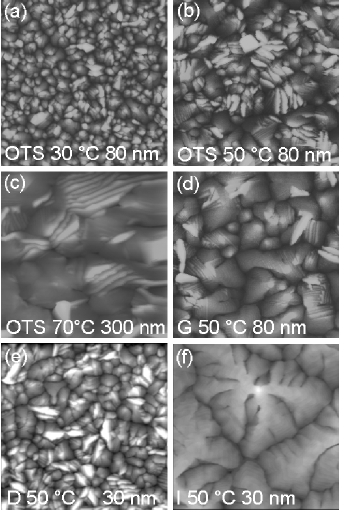
Pentacene films deposited at higher substrate temperature often consist of large grains Hajlaoui et al. (2002). The larger grain size forming at higher temperatures on OTS treated substrates is shown in the topography images in Fig. 5(a)-(c). The images show evidence of lamellar growth and the brightest spots mark grains with a height well above the average film thickness. Those grains consist presumably of flat lying pentacene molecules Shtein et al. (2002)Gundlach et al. (2004). The height of those grains increases with increasing deposition temperature, indicating a rapid growth of grains in the a-b plane. A typical image of a film deposited onto a phenyl treated (G) substrate is shown in Fig. 5(d) and reveals larger grains than obtained for films on OTS treated substrates held at the same deposition temperature (cf. Fig. 5(b)). Additionally, the density of edge oriented grains (resulting from flat lying molecules) is smaller for films deposited onto substrates treated with (G). In Fig. 5(e) and 5(f) topography images of films deposited onto substrates treated with (D) and (I) show an opposite relationship between the mobility and the grain size: although the grain size of film (D) is smaller compared to (I), the transistors on (D) show a larger mobility than the one on (I) (cf. Tab. 1). It is worthwhile emphasizing that the film morphology as observed with AFM does not necessarily reflect the microstructure of the first few monolayers of pentacene that forms the electrically active channel.


The XRD patterns in Fig. 6 reveal the over-all
difference in film morphology: pentacene films generally show two
distinct crystalline phases with different d-spacings, a ”thin
film phase” with 15.4 Å (00) and a ”single crystal
phase” with 14.4 Å (00)
Dimitrakopoulos
et al. (1996)Bouchoms et al. (1999)Mattheus et al. (2003). The
films deposited at 30 ∘C crystallize in the ”thin film
phase” only, while the ”single crystal phase” is more prevalent in
the films deposited at higher substrate temperatures Lin et al. (1997b)
(cf. Fig. 6(a)). For the OTS devices, the hole
mobility is slightly higher in the latter as can be seen from Tab.
2. This is in agreement with results reported in
e.g. Knipp et al. (2003), and is presumably due to better overlap of
the -orbitals Brédas et al. (2002) of the pentacene molecules. In
Fig. 6(b) the mixture of the ”thin film phase” and the
”single crystal phase” is shown for treatments (B), (C), (E) and
(H). Here the pentacene films have been deposited on substrates
held at 50 ∘C and interestingly, a different trend is
observed for treatments (C) and (B): TFTs on SAM (B) show a lower
mobility although the single crystal phase is more dominant. From
a comparison of the results in Tab. 2 we
conclude that the variations of the TFT characteristics (, ) are dominated by the particular
organosilanes forming the SAM and not by the over-all film
morphology as probed by XRD and AFM. This conclusion is supported
by the single crystal experiments described later.
III.2 Effect of the SAM’s dipole field
The observed shifts in the electrical characteristics correspond to the electron acceptance properties of the organosilane molecule’s end group. For treatment (C) with the CH2Cl end group for instance, this means that electrons from the pentacene film are attracted by the SAM leaving behind mobile holes in the channel. Thus a more positive gate bias is needed to switch off the device, i.e. shifts towards more positive values.
The electronegativity of the molecule’s functional group influences the charge distribution within the molecule and can lead to the formation of an electric dipole. Campbell et al. Campbell et al. (1996) calculated the charge distribution within similar molecules using an ab initio scheme and found a dipole moment whose strength depends on the functional group of the investigated molecule. When such molecules form a SAM the molecular dipoles gives rise to a net polarization of the SAM that changes the surface potential Ishii et al. (1999) as verified with Kelvin-probe measurements in Campbell et al. (1996) and by Kelvin-probe force microscopy in Sugimura et al. (2002). In Sugimura et al. (2002) the authors calculated dipole moments of 0.5 and -1 Debye for isolated molecules similar to (A) and (F), and measured a surface potential difference of approximately 0.2 V between the corresponding SAMs formed on SiO2. Assuming the thickness of the SAMs to be 2 nm, this corresponds to an electric field of 1 MV/cm. To produce the same field by applying a voltage across the 300 nm thick SiO2 gate insulator a gate voltage of 30 V is necessary, which corresponds well with the shifts in transfer characteristics we measure in our devices (cf. Tab. 1).
In the presented situation the charge density respectively the energy levels need to be considered in a self-consistent way, resulting from the properties of the individual molecule in the SAM attached to silica, and the adjacent pentacene molecules. This is important because it has been shown in e.g. Vager and Naaman (2002) that the electronic properties of a close-packed organized organic monolayer can differ from the properties of the isolated molecule. Additionally our samples were exposed to ambient air where water can adsorb on the surface which might affect the effective dipole strength of the SAM.

The change in surface potential modifies the interface properties
as illustrated in the schematic band diagram shown in Fig.
7. When pentacene is deposited onto SiO2 under
UHV conditions, the vacuum levels are aligned and no bending of
the highest occupied molecular orbital (HOMO) and lowest
unoccupied molecular orbital (LUMO) level occurs Watkins and Gao (2003)
as illustrated in Fig. 7(a). For simplicity, only
the gate electrode’s Fermi level is shown. When a negative gate
voltage is applied the Fermi level of the gate electrode shifts
towards higher (electron) energies. Part of the applied gate
voltage is dropped across the gate insulator, and since the band
alignment of the HOMO and LUMO level is fixed with respect to the
vacuum level, the remaining gate voltage bends the HOMO and the
LUMO levels. Therefore mobile charge carriers can accumulate and
form the conducting channel. For a SAM with a permanent electric
dipole field inserted between the gate insulator and the
pentacene, the situation is as illustrated in Fig.
7(b): the dipole field of the SAM modifies the
surface potential which has the same effect as applying a
(negative) gate voltage. The solid curves in Fig.
7(b) appear to be valid for all treatments except
the phenyl treatment (G). For this treatment the situation may be
depicted with the dotted curves where the majority carriers are
depleted. Fig. 7(c, d) depict the situation where a
negative gate voltage is applied to devices with (Fig.
7(d)) and without (Fig. 7(c)) a SAM:
the gate voltage rises the vacuum level of the gate insulator and
additionally it is raised by the permanent dipole field of the
SAM, resulting in an increased band bending and therefore in an
increased hole density in the channel. As a consequence, the
turn-on and the threshold voltage are determined by the surface
potential of the layer next to the transistor channel. We
emphasize that any surface charge present at the gate insulator
due to a contact potential Tsividis (1999) or imperfections such
as oxygen (OH-groups), water moleculesNicollian and Brews (1991) or mobile
ions Rep et al. (2003) also influences the surface potential and
therefore influences the threshold voltage and the turn-on
voltage; especially in devices with untreated oxide
Gundlach et al. (2004). Thus Fig. 7 may capture only part
of the total situation relevant for the device performance.

The mobile charge carrier density induced by the SAM ()
is shown for the various SAMs in Fig. 8. The density
was estimated using , with
nF/cm2 being the measured insulator capacitance
per unit area and the elementary charge. The turn-on voltage
is chosen as it is a measure of the hole concentration in the
channel at zero gate bias: applying the turn-on voltage to the
gate electrode depletes the channel and the bulk pentacene as much
as possible. Using the flat band voltage would give a more
accurate estimate but it is not accessible from our measurements.
Since the pentacene films are assumed to be thinner than the
screening length near flat band condition Greve (1998), we
expect that the turn-on voltage is very close to the flat band
voltage. The maximum carrier concentration corresponds to about
one induced mobile hole per 100 SAM molecules, assuming a surface
density of the SAM molecules of /cm2
Vuillaume et al. (1996).
III.3 Density of States, Threshold Voltage and Additional Trap States
A more microscopic approach taking into account the
imperfections of the semiconductor is desirable. Following
Völkel et al. V lkel et al. (2002) the mobile holes observed at
zero gate bias can be modeled using electron acceptor
states in the band gap close to the HOMO level. Such
acceptor states move the Fermi level closer to the HOMO
level by changing the thermodynamic equilibrium position of
the Fermi level close to the gate insulator. Völkel and
co-workers V lkel et al. (2002) used a one-dimensional
transistor model to study the effects of localized band-gap
states on the electrical characteristics of pentacene TFTs.
The authors introduced acceptor states at the interface
layer next to the gate insulator in order to explain their
observed shifts in turn-on voltage, and donor states to
account for the shifts in threshold voltage. A total trap
density of /cm3 accounts for the
observed shifts. Assuming a channel thickness of 5 nm and a
homogeneous carrier density in the channel, the acceptor
concentration in their model corresponds to a surface
charge density of /cm2, close to our
results given in Fig. 8.
With increasing negative gate voltage, more trap states are filled. If all deep traps are filled and the local Fermi energy in the channel is in the energy range of the transport level (the energy at which thermal activation begins to predominate) Monroe (1985)Arkhipov et al. (2003) the threshold voltage is reached Shur and Hack (1984)Lang et al. (2004). Horowitz and Delannoy expressed this condition as the equilibrium between trapped and mobile carriers Horowitz and Delannoy (1991) (for a refinement see Balakrishnan et al. (2003)). Therefore the threshold voltage is tied to the turn-on voltage via the trap density, and the threshold voltage above turn-on voltage () is an estimate of the trap density in the channel.
Estimating the number of trap states from the threshold voltage above turn-on voltage we find the total trap density using where is again the oxide capacitance per unit area. This results in a trap density of /cm2. Taking into account only transistors with mobilities greater than 0.5 cm2/Vs the trap density in the channel is estimated to be /cm2. The values are in good agreement with values derived from simulations reported in V lkel et al. (2002).
The origin of the increased trap density cannot clearly be
revealed by these experiments. Our control experiments
suggest that the effect of the SAM dominates over the
effect of film morphology. Increased trap densities were
also found in polymer devices with a high-k gate insulator
compared to low-k gate insulators and were ascribed to a
dipolar disorder caused broadening of the Gaussian
distributed transport states Veres et al. (2003). In
Kadashchuk et al. (1993) the authors report on dipole impurities
in anthracene single crystals and suggest that traps are
formed as a result of the interaction of carriers with the
dipole moment of the impurities. Similarly, the
introduction of dipole moments between gate insulator and
pentacene might change the local polarization of individual
pentacene molecules, therefore introducing new trap states
Silinsh and V. Čápek (1994).
III.4 Single Crystal Experiments
To verify that the dipole field of the SAM governs the turn-on voltage, and to test whether or not the strong dipole moment of the SAM molecules can influence the trap distribution of single crystal FETs (SC-FETs) we fabricated SC-FETs using the ”flip-crystal” technique Takeya et al. (2003)R. W. I. de Boer et al. (2003). Rubrene crystals were used because large planar crystals can be grown as described in e.g. Goldmann et al. (2004), and because rubrene shows a very high mobility Williams (1997)Goldmann et al. (2004)Sundar et al. (2004). The wafers were treated with (A) or (E) and the resulting transistors have a on/off ratios and a mobility cm2/Vs, indicating that the presence of the SAM has little or no influence on the effective mobility. It also suggests that the low mobility of TFTs with treatment (E) is probably caused by a poor molecular ordering as revealed by XRD measurements.
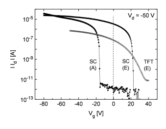
The transfer characteristics of the SC-FETs in Fig. 9 are offset by 39 V while basically maintaining the shape of the subthreshold region. Similar results for SC-FETs have recently been reported by Takeya et al. J. Takeya et al. (2004). Also in Fig. 9, we show the transfer characteristic of a typical thin film device with treatment (E). The curve for the thin film transistor was normalized to account for the different W/L ratios. A detailed analysis of the subthreshold region shows a very steep subthreshold swing of 0.3 V/dec (300 nm SiO2) for the SC-FET treated with (E), and a slightly larger subthreshold swing of 0.5 V/dec for the SC-FET with (A). The significantly steeper subthreshold swing of the single crystal devices compared to that of the thin film devices indicates a significantly lower trap density for single crystal FETs.
The off-current in both single crystal devices is similar, while it is an order of magnitude higher in the thin film device, indicating that the off-current in the TFT could be limited by bulk traps V lkel et al. (2002)D. Oberhoff et al. (2004).
While the behavior of the thin film devices can be modeled using a flexible density of states model as shown in V lkel et al. (2002)D. Oberhoff et al. (2004), modeling the single crystal devices proves difficult. However, shifting the transfer characteristic by V while maintaining a steep subthreshold swing is difficult to achieve in a ”trap-only” model, since the the amount of acceptor states necessary to shift the turn-on voltage also degrades the subthreshold swing. We take this as compelling evidence that the observed shifts of the threshold voltage and the turn-on voltage are caused by the built-in electric field of the self assembled monolayers.
IV Conclusions
We fabricated pentacene thin film transistors and rubrene single crystal FETs incorporating nine organosilanes with different functional groups. The organosilanes form self assembled monolayers on the SiO2 gate insulator and have various dipole moments depending on the electron acceptance properties of their functional group. We find the dipole moment of the SAM modifies the surface potential of the layer next to the transistor channel and induces mobile charge carriers at zero gate bias. This manifests itself in a shift of the transfer characteristics. A simple energy level diagram is used to explain these observations. Similar shifts have been modeled by Völkel et al. V lkel et al. (2002) using appropriate trap state distributions. From the difference between the threshold voltage and the turn-on voltage we estimate the trap density in the thin film FETs to be of order /cm2, while a lower trap density is found for rubrene single crystal FETs. The single crystal experiments clearly show that the built-in electric field of a self assembled monolayer next to the transistor channel acts as a gate bias and modulates the charge carrier density.
Acknowledgements.
The authors would like to thank Kurt Mattenberger and Hans-Peter Staub for technical solutions, Cornelius Krellner for crystal growth and A. Stemmer for providing access to the AFM equipment. Fruitful discussions with Benjamin Rössner, H. Bässler, G. Horowitz, T. N. Jackson, E. J. Meijer, G. Paasch, S. Scheinert and K. Seki are gratefully acknowledged. Further we would like to thank Urs Notter and the other members of the machine shop of the ETH Physics Departement. This study is partly supported by ETH grant 20020-02, by the Swiss National Science Foundation, and by the Swiss BBW as part of the EU-Research program EUROFET (HPRN-CT-2002-00327).References
- Klauk et al. (2002) H. Klauk, M. Halik, U. Zschieschang, G. Schmid, W. Radlik, and W. Weber, J. Appl. Phys. 92, 5259 (2002).
- Kelley et al. (2003) T. W. Kelley, D. V. Muyres, P. F. Baude, T. P. Smith, and T. D. Jones, Mat. Res. Soc. Symp. Proc. 771, L6.5.1 (2003).
- Moore (2002) S. K. Moore, IEEE Spectrum 39, 55 (2002).
- Knipp et al. (2003) D. Knipp, R. A. Street, A. V lkel, and J. Ho, J. Appl. Phys. 93, 347 (2003).
- Salleo and Street (2003) A. Salleo and R. A. Street, J. Appl. Phys. 94, 471 (2003).
- Street et al. (2003) R. A. Street, A. Salleo, and M. L. Chabinyc, Phys. Rev. B 68, 085316 (2003).
- Northrup and Chabinyc (2003) J. E. Northrup and M. L. Chabinyc, Phys. Rev. B 68, 041202 (2003).
- Gomes et al. (2004) H. L. Gomes, P. Stallinga, F. Dinelli, M. Murgia, F. Biscarini, D. M. de Leeuw, T. Muck, J. Geurts, L. W. Molenkanp, and V. Wagner, Appl. Phys. Lett. 84, 3184 (2004).
- V lkel et al. (2002) A. R. V lkel, R. A. Street, and D. Knipp, Phys. Rev. B 66, 195336 (2002).
- Katz et al. (2002) H. E. Katz, X. M. Hong, A. Dodabalapur, and R. Sarpeshkar, J. Appl. Phys. 91, 1572 (2002).
- Li et al. (2002) T. Li, J. W. Balk, P. P. Ruden, I. H. Campbell, and D. L. Smith, J. Appl. Phys. 91, 4312 (2002).
- Schroeder et al. (2003) R. Schroeder, L. A. Majewski, and M. Grell, Appl. Phys. Lett. 83, 3201 (2003).
- Lin et al. (1997a) Y.-Y. Lin, D. J. Gundlach, S. F. Nelson, and T. N. Jackson, IEEE Trans. Electron Dev. 18, 1325 (1997a).
- Salleo et al. (2002) A. Salleo, M. L. Chabinyc, M. S. Yang, and R. A. Street, Appl. Phys. Lett. 81, 4383 (2002).
- Kobayashi et al. (2004) S. Kobayashi, T. Nishikawa, T. Takenobu, S. Mori, T. Shimoda, T. Mitani, H. Shimotani, N. Yoshimoto, S. Ogawa, and Y. Iwasa, Nat. Mater. 3, 317 (2004).
- McGovern et al. (1994) M. E. McGovern, K. M. R. Kallury, and M. Thompson, Langmuir 10, 3607 (1994).
- Tillman et al. (1988) N. Tillman, A. Ulman, J. S. Schildkraut, and T. L. Penner, J. Am. Chem. Soc. 110, 6136 (1988).
- Angst and Simmons (1991) D. L. Angst and G. W. Simmons, Langmuir 7, 2236 (1991).
- Goldmann et al. (2004) C. Goldmann, S. Haas, C. Krellner, K. P. Pernstich, D. J. Gundlach, and B. Batlogg, J. Appl. Phys. 96, 2080 (2004).
- Sze (1988) S. M. Sze, Physics of Semiconductor Devices (Wiley Eastern Limited, 1988).
- Meijer et al. (2002) E. J. Meijer, C. Tanase, P.W. M. Blom, E. van Veenendaal, B.-H. Huisman, D. M. de Leeuw, and T. M. Klapwijk, Appl. Phys. Lett 80, 3838 (2002).
- Shtein et al. (2002) M. Shtein, J. Mapel, J. B. Benziger, and S. R. Forrest, Appl. Phys. Lett. 81, 268 (2002).
- Gundlach et al. (2004) D. J. Gundlach, L. Zhou, J. A. Nichols, C. D. Sheraw, C.-C. S. Kuo, and T. N. Jackson, to be published (2004).
- Tanase et al. (2003) C. Tanase, E. J. Meijer, P. M. Blom, and D. M. de Leeuw, Org. Electron. 4, 33 (2003).
- Dinelli et al. (2004) F. Dinelli, M. Murgia, P. Levy, M. Cavallini, F. Biscarini, and D. M. de Leuw, Phys. Rev. Lett. 92, 116802 (2004).
- Hajlaoui et al. (2002) M. E. Hajlaoui, F. Garnier, L. Hassine, F. Kouki, and H. Bouchriha, Synthetic Met. 129, 215 (2002).
- Dimitrakopoulos et al. (1996) C. D. Dimitrakopoulos, A. R. Brown, and A. Pomp, J. Appl. Phys. 80, 2501 (1996).
- Bouchoms et al. (1999) I. P. M. Bouchoms, W. A. Schoonveld, J. Vrijmoeth, and T. M. Klapwijk, Synthetic Met. 104, 175 (1999).
- Mattheus et al. (2003) C. C. Mattheus, A. B. Dros, J. Baas, G. T. Oostergetel, A. Meetsma, J. L. de Boer, and T. T. M. Palstra, Synthetic Met. 138, 475 (2003).
- Lin et al. (1997b) Y.-Y. Lin, D. J. Gundlach, S. F. Nelson, and T. N. Jackson, IEEE Electr Device L. 18, 606 (1997b).
- Brédas et al. (2002) J. L. Brédas, J. P. Calbert, D. A. da Silva Filho, and J. Cornil, PNAS 99, 5804 (2002).
- Campbell et al. (1996) I. H. Campbell, S. Rubin, T. A. Zawodzinski, J. D. Kress, R. L. Martin, D. L. Smith, N. N. Barashkov, and J. P. Ferraris, Phys. Rev. B 54, 14321 (1996).
- Ishii et al. (1999) H. Ishii, K. Sugiyama, E. Ito, and K. Seki, Adv. Mater. 11, 605 (1999).
- Sugimura et al. (2002) H. Sugimura, K. Hayashi, N. Saito, N. Nakagiri, and O. Takai, Appl. Surf. Sci. 188, 403 (2002).
- Vager and Naaman (2002) Z. Vager and R. Naaman, Chem. Phys. 281, 305 (2002).
- Watkins and Gao (2003) N. J. Watkins and Y. Gao, J. Appl. Phys. 94, 5782 (2003).
- Tsividis (1999) Y. Tsividis, Operation and modeling of the MOS transistor (WCB McGraw-Hill, 1999), 2nd ed.
- Nicollian and Brews (1991) E. H. Nicollian and J. R. Brews, MOS (Metal Oxide Semiconductor) Physics and Technology (John Wiley & Sons, 1991).
- Rep et al. (2003) D. B. A. Rep, A. F. Morpurgo, W. G. Sloof, and T. M. Klapwijk, J. Appl. Phys. 93, 2082 (2003).
- Greve (1998) D. W. Greve, Field effect devices and applications: Devices for portable, low-power, and imaging systems (Prentice Hall Series in Electronics and VLSI, 1998).
- Vuillaume et al. (1996) D. Vuillaume, C. Boulas, J. Collet, J. V. Davidovits, and F. Rondelez, Appl. Phys. Lett. 69, 1646 (1996).
- Monroe (1985) D. Monroe, Phys. Rev. Lett. 54, 146 (1985).
- Arkhipov et al. (2003) V. I. Arkhipov, J. Reynaert, Y. D. Jin, P. Heremans, E. V. Emelianova, G. J. Adriaenssens, and H. B ssler, Synth. Met. 138, 209 (2003).
- Shur and Hack (1984) M. Shur and M. Hack, J. Appl. Phys. 55, 3831 (1984).
- Lang et al. (2004) D. V. Lang, X. Chi, T. Siegrist, A. M. Sergent, and A. P. Ramirez (2004), eprint cond-mat/0312722.
- Horowitz and Delannoy (1991) G. Horowitz and P. Delannoy, J. Appl. Phys. 70, 469 (1991).
- Balakrishnan et al. (2003) R. V. R. Balakrishnan, A. K. Kapoor, V. Kumar, S. C. Jain, R. Mertens, and S. Annapoorni, J. Appl. Phys. 94, 5302 (2003).
- Veres et al. (2003) J. Veres, S. D. Ogier, S. W. Leeming, D. C. Cupertino, and S. M. Khaffaf, Adv. Funct. Mater. 13, 199 (2003).
- Kadashchuk et al. (1993) A. K. Kadashchuk, N. I. Ostapenko, Yu. A. Skryshevskiĭ, V. I. Sugakov, T. O. Susokolova, and M. T. Shpak, Phys. Solid State 35, 840 (1993).
- Silinsh and V. Čápek (1994) E. A. Silinsh and V. Čápek, Organic Molecular Crystals: Interaction, Localization, and Transport Phenomena (AIP Press New York, 1994).
- Takeya et al. (2003) J. Takeya, C. Goldmann, S. Haas, K. P. Pernstich, B. Ketterer, and B. Batlogg, J. Appl. Phys. 94, 5800 (2003).
- R. W. I. de Boer et al. (2003) R. W. I. de Boer, T. M. Klapwijk, and A. F. Morpurgo, Appl. Phys. Lett. 83, 4345 (2003).
- Williams (1997) W. G. Williams, Discuss. Faraday Soc. 51, 61 (1997).
- Sundar et al. (2004) V. C. Sundar, J. Zaumseil, V. Podzorov, E. Menard, R. L. Willett, T. Someya, M. E. Gershenson, and J. A. Rogers, Science 303, 1644 (2004).
- J. Takeya et al. (2004) J. Takeya et al., in press (2004).
- D. Oberhoff et al. (2004) D. Oberhoff et al., to be published (2004).