Radio-frequency operation of a double-island single-electron transistor
Abstract
We present results on a double-island single-electron transistor (DISET) operated at radio-frequency (rf) for fast and highly sensitive detection of charge motion in the solid state. Using an intuitive definition for the charge sensitivity, we compare a DISET to a conventional single-electron transistor (SET). We find that a DISET can be more sensitive than a SET for identical, minimum device resistances in the Coulomb blockade regime. This is of particular importance for rf operation where ideal impedance matching to transmission lines is only possible for a limited range of device resistances. We report a charge sensitivity of for a rf-DISET, together with a demonstration of single-shot detection of small () charge signals on timescales.
I Introduction
With the continued miniaturization of microelectronics facing serious limitations due to quantum effects and heat dissipation, alternative computing paradigms are envisaged. These include solid-state quantum computers Orlov et al. (1997); Shnirman et al. (1997); Kane (1998); Makhlin et al. (1999); Vrijen et al. (2000) and quantum-dot cellular automata (QCA),Lent et al. (1993) which promise a further increase in integration and computing power beyond such limitations. In these new architectures, readout of a computational result often requires detection of charge motion on fast timescales – not only to ensure fast processing speeds, but also to perform a readout operation before the information is lost due to interaction with the environment or relaxation. Towards this goal, the suitability of radio-frequency single-electron transistors (rf-SETs) as fast and sensitive charge detectors has been demonstrated.Schoelkopf et al. (1998); Korotkov and Paalanen (1999); Devoret and Schoelkopf (2000); Aassime et al. (2001)
Recently double-island SETs (DISETs) have been proposed for readout of QCA and qubits.Macucci et al. (2001); Tanamoto and Hu (2004) With such applications in mind, Brenner et al. have shown that in addition to conventional charge sensing (like with the single-island SET), DISETs can also be used to sense rapid transitions between electrostatically degenerate charge states.Brenner et al. (2003a, b) The latter, novel mode of operation suggests that DISETs may be useful for readout of a QCA cell or a qubit in a basis other than the charge position basis. In particular, both types of detection can be achieved in the same device, simply by using different biasing regimes: keeping the DISET at a high transconductance or at a conductance peak (with zero transconductance), respectively. This versatility alone makes DISET detectors an interesting alternative to conventional SET detectors.
In this article we report work on a radio-frequency DISET (rf-DISET), including a measurement of its charge sensitivity and the demonstration of single-shot measurements on timescales. Operation at radio-frequencies increases the sensitivity of charge detectors as -type noise becomes negligible (i.e. less than the detector noise) and also facilitates the study of processes that have short decay or relaxation times, such as qubits. We also present an intuitive model for calculating the charge sensitivity of a DISET, and we find that under certain conditions the charge sensitivity of a DISET is superior to that of a SET. We consider the case where the minimum device resistances and source-drain biases are identical for both devices. This is an important comparison since rf operation imposes restrictions on the minimum device resistance needed to achieve optimum impedance matching with a reasonable quality factor.
II DISET charge sensitivity
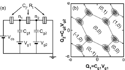
DISETs – originally introduced as single-electron pumps by Pothier et al.Pothier et al. (1992) – consist of two small islands in series, connected by ultra-small tunnel-junctions to each other and to source and drain leads (see circuit diagram in Fig. 1a). Their operation is governed by Coulomb blockade (CB) effects,Grabert and Devoret (1992) allowing voltages applied to capacitively coupled gates to alter the integer number of excess electrons on island 1(2), , in steps of . Figure 1b shows that the stable DISET charge configuration domains exhibit a typical “honeycomb” characteristic as a function of two gate voltages, and . Current can flow through the device at triple-points, where three charge configuration domains adjoin. Current peaks for non-zero temperature are indicated by contours encircling the triple-points in Fig. 1b. We refer the reader to the review by van der Wiel et al. for a more thorough discussion of the operation of DISETs.van der Wiel et al. (2003)
Like in conventional SETs, the DISET conductance is extremely sensitive to small induced charge signals. In the following paragraphs we give a practical, intuitive definition for the DISET charge sensitivity and compare it to that of a SET in order to identify potential advantages of a DISET over a SET. In general, the charge sensitivity of a detector can be defined through its current response to an induced charge signal in the presence of noise, expressed by the current-noise spectral density ,Korotkov (1996)
| (1) |
or, equivalently, by the charge noise level in a measurement bandwidth ,
| (2) |
For a SET, the source-drain current is a periodic function of the induced charge, , where is the number of excess electrons on the SET island. A DISET on the other hand has two islands, which sense an effective charge and , respectively. The DISET current is thus a periodic function of the induced charges on both islands, . In an idealized case, the effective induced charge on one island is proportional to the other, . Two special cases are considered here: (e.g. single gate or chargeable object coupled equally strongly to both islands) and (e.g. polarisable object parallel to the DISET, such as the double-dot in Fig. 3 and Refs. Brenner et al., 2003a, b). The current is then a function of the induced charge on only one of the islands for both values of , , and can be considered the response to a relevant induced charge signal .oth
Based on this definition of the relevant induced charge, we calculate the (normal-state) dc source-drain current and differential current of a DISET and compare them to those of a SET. The dc source-drain currents are obtained from the stationary solutions of the respective master equations in the two-state (SET) or three-state (DISET) approximation.mas Here, the following assumptions are made:
-
•
All tunnel junctions capacitances are identical;
-
•
The minimum device resistances for the SET and the DISET in the CB regime are identical ( is the resistance of a single junction and is the number of junctions in the respective device);
-
•
The absolute induced charges are identical for all islands;
-
•
The temperature is low compared to the charging energy of a single junction: (here );
-
•
The source-drain bias is small – i.e. (linear response) – and identical for both devices; and
-
•
Cotunneling is disregarded.
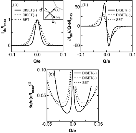
Figure 2a shows the respective centered dc current peaks for a SET and a DISET for and as a function of . The currents are normalized to the maximum peak current . In the case of a DISET, the induced charges on the islands are ; i.e. a triple-point in the honeycomb diagram of the DISET is traversed either from the top-left to the bottom-right () or from the bottom-left to the top-right (), as indicated in the inset. The differential currents (normalized to ) are shown in Fig. 2b, indicating that the maximum value is achieved for a DISET with . Note that the DISET peak for is asymmetric and has a higher transconductance on one side of the peak than on the other. This needs to be taken into consideration measurements that require maximum charge sensitivity.
Ultimately, the noise in single-electron devices is limited by shot noise with the noise-current spectral density
| (3) |
where is the Fano factor accounting for shot noise suppression or enhancement effects. The charge sensitivities as a function of where calculated for . Figure 2c shows that the charge sensitivity of a DISET is better than that of a SET by a factor of up to for identical maximum peak currents and for the assumptions made above. This is of particular interest in light of the restrictions for associated with rf operation. The intuitive picture presented here was used as a basis to determine the charge sensitivity of a rf-DISET for experimentally.
There are two other effects, which are not included in the model presented here and which may also lead to an enhanced sensitivity for the DISET in comparison to single-island devices. Firstly, the different Fano factors for DISETs and SETs may lead to a further reduction of shot noise in the DISET compared to the SET. The shot noise level in DISETs can be suppressed by a factor of up to ,Eto (1996); Korotkov and Likharev (2000); Gattobigio et al. (2002) compared to for SETs.Hanke et al. (1994); Birk et al. (1995) Secondly, additional shot noise due to cotunneling is also suppressed in DISETs (compared to SETs) due to the additional tunnel junction.Averin and Odintsov (1989); Averin and Nazarov (1990) Both of the above effects are strongly dependent on the source-drain bias, the induced charge and the junction parameters.
III rf-DISET setup and operation
Motivated by the possibility of increased sensitivity, we now turn to discuss our experiment on the rf-DISET. The experimental setup employed for this work is schematically shown in Fig. 3, which also shows a scanning electron micrograph of the DISET device (the double-dot adjacent to the DISET was not used in these experiments). The device was fabricated using standard shadow evaporation of aluminum with in-situ oxidation.Fulton and Dolan (1987)
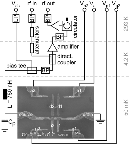
Fast operation is made possible by including the DISET in an impedance-matching LCR tank circuit – a technique pioneered by Schoelkopf et al. for conventional SETs made of aluminum.Schoelkopf et al. (1998) The rf carrier signal and a dc source-drain bias were coupled into an impedance matching LCR tank circuit,Pozar (1998) consisting of commercially available chip inductors (impedance ), a parasitic capacitance to ground () and the total DISET resistance . Using an impedance of , the resonance frequency of the tank circuit was set to within the operating bandwidth of the rf amplifiers. The reflection coefficient for the rf signal reflected from the tank circuit is a function of (as are the quality factor and the bandwidth of the tank circuit). In the case of perfect matching, when the DISET is at a conductance maximum and when it is blockaded. The optimization of the matching and the performance of the detector system as a whole imposes limitations on the choices for the minimum device resistance (here: perfect matching for ). The device presented in this paper had a minimum device resistance of in the CB regime, which resulted in a slightly mismatched tank-circuit.
The reflected rf signal was amplified by a cryogenic, ultra-low-noise rf amplifier ber and a low-noise rf amplifier at room-temperature. A circulator prevented noise at the front-end of the room-temperature amplifier from propagating to the cryogenic amplifier. For time-domain measurements, the signal was demodulated and fed into a multichannel oscilloscope, while for frequency-domain measurements, the reflected signal was fed into a spectrum analyzer. The gates were modulated on fast timescales using a synthesized function generator and/or on slow timescales using digital-to-analog converters. A magnetic field of 0.5 T was applied to suppress superconductivity in the aluminum.
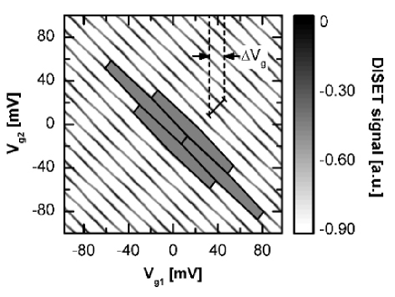
By applying a triangular modulation signal to gate g1 () and stepping on a 1-s timescale, the characteristic honeycomb diagram of the DISET was obtained from the demodulated, reflected rf signal (Fig. 4). The observed non-zero conductance (gray) along the edges of the honeycombs is likely due to cotunneling. This is consistent with relatively low junction resistances of order , estimated from the room-temperature resistance of .
IV Experimental results
To determine the charge sensitivity of the rf-DISET, its response (in terms of the reflected power) to a g-gate signal with amplitudes was measured in both the frequency domain and the time domain. The period of CB oscillations for this case, (indicated in Fig. 4), corresponded to the addition of one electron to each island. Hence, the effective induced charge was given by . Constant offset voltages were applied to the a-gates to bias the DISET to a point of maximum transconductance.
For measurement in the frequency-domain, an equivalent (rms) signal was applied to the g-gates at various modulation frequencies , and using a carrier signal at the resonance frequency of the tank circuit. A spectrum analyzer was used to measure the signal-to-noise ratio (SNR) of the amplitude modulation side-bands. Using
| (4) |
the charge sensitivity was obtained as a function of (Fig. 5). The data shown contains a number of individual data sets, which were recorded at different resolution bandwidths of the spectrum analyzer. Due to uncertainties in the noise level, the worst obtained SNR was considered the most meaningful figure when determining the actual charge sensitivity. For modulation frequencies below , the charge sensitivity was reduced due to -type noise – here, with a dependence of the noise power. Above approximately 50 kHz, amplifier noise dominated, resulting in an estimated charge sensitivity of .
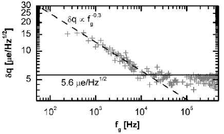
This initial result is comparable to the best charge sensitivities obtained in rf-SET setups to date: The best such sensitivity of was achieved by Aassime et al. in a rf-SET in the superconducting state.Aassime et al. (2001, 2002) Buehler et al. achieved charge sensitivities of and in two simultaneously operated rf-SETs in a twin-rf-SET experiment.Buehler (2003); Buehler et al. (2004); Buehler et al. (2003a) The DISET charge sensitivity reported here is all the more encouraging since the junction parameters were not ideal for optimum device performance. Better impedance matching of the tank circuit also promises further improvement of the DISET charge sensitivity.
In order to demonstrate charge detection on fast timescales, a square wave signal with 50 kHz modulation frequency and equivalent amplitude was applied to the g-gates (Fig. 6a). The demodulated, reflected signal was amplified and low-pass filtered (1 MHz) before being detected by an oscilloscope. Figure 6b shows the response of the DISET in a single-shot measurement for a measurement time of . From the average half-width of the Gaussian distributions fitted to the histogram of the data (Fig. 6c), the charge noise was estimated to . With the measurement bandwidth and Eq. (2), an estimate for the time-domain charge sensitivity of was obtained.
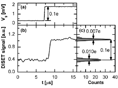
Longer measurement times are required in order to detect smaller charge signals with a minimum error rate. In the presence of type noise, however, the Gaussian distributions increasingly overlap with measurement time, which increases the error probability of a single-shot measurement and in turn imposes limitations on the smallest detectable charge signals for a given, tolerable error probability Buehler (2003); Buehler et al. (2003b). The discrepancy to the frequency-domain charge sensitivity can be attributed to additional noise in the demodulation circuit and the oscilloscope used in time-domain measurements. These noise contributions have to be minimized in order to obtain a time-domain sensitivity similar to the frequency-domain sensitivity. This was achieved to a good degree by Bladh et al. who reported a time-domain sensitivity of approximately , compared to a frequency-domain sensitivity of .Bladh et al. (2003) We also note that the frequency-domain charge sensitivity of the present rf-DISET was not limited by shot noise but rather by amplifier noise and other noise sources in the rf network.
In order to quantify the system noise, the noise temperature was measured according to the method described in Ref. Aassime et al., 2001 and assuming a Fano factor of . We obtain a noise temperature of , which is lower than previously reported noise temperatures of .Aassime et al. (2001); Buehler (2003); Roschier et al. (2004) The individual contributions of components to the noise in the rf network were not explicitly studied in this work. However, the largest contribution stems from the cryogenic amplifier (according to its specifications approximately 1.6 K at 20 K and possibly less at 4.2 K). The remaining contributions are attributed to the imperfectly matched impedance of the tank circuit to the rf network, the room-temperature rf amplifier and losses and reflections elsewhere in the network.
V Conclusion
Motivated by a possible enhancement in charge sensitivity in comparison to conventional SETs, we have presented experimental results on a novel rf-DISET detector. In certain circumstances we find that DISETs can improve the charge sensitivity by a factor of 2.23 without increasing the minimum device resistance required for optimum impedance matching. Our experimental results indicate a charge sensitivity of , and a single-shot time-domain sensitivity of . The noise temp of our entire system was measured to be 2.1 K. The capability of DISETs to detect both well-defined and electrostatically degenerate charge configurations, may make DISETs an interesting alternative to conventional SETs for readout of QCA-type devices and qubits in solid-state quantum computer architectures.
Acknowledgements
The authors would like to thank R. P. Starrett and D. Barber for technical assistance and A. D. Greentree, A. R. Hamilton and A. N. Korotkov for helpful discussions. This work was supported by the Australian Research Council, the Australian government and by the US National Security Agency (NSA), Advanced Research and Development Activity (ARDA) and the Army Research Office (ARO) under contract number DAAD19-01-1-0653.
References
- Orlov et al. (1997) A. O. Orlov, I. Amlani, G. H. Bernstein, C. S. Lent, and G. L. Snider, Science 277, 928 (1997).
- Shnirman et al. (1997) A. Shnirman, G. Schön, and Z. Hermon, Phys. Rev. Lett. 79, 2371 (1997).
- Kane (1998) B. E. Kane, Nature 393, 133 (1998).
- Makhlin et al. (1999) Y. Makhlin, G. Schön, and A. Shnirman, Nature 398, 305 (1999).
- Vrijen et al. (2000) R. Vrijen, E. Yablonovitch, K. Wang, H. W. Jiang, A. Balandin, V. Roychowdhury, T. Mor, and D. DiVincenzo, Phys. Rev. A 62, 012306 (2000).
- Lent et al. (1993) C. S. Lent, P. D. Tougaw, W. Porod, and G. H. Bernstein, Nanotechnology 4, 49 (1993).
- Schoelkopf et al. (1998) R. J. Schoelkopf, P. Wahlgren, A. A. Kozhevnikov, P. Delsing, and D. E. Prober, Science 280, 1238 (1998).
- Korotkov and Paalanen (1999) A. N. Korotkov and M. A. Paalanen, Appl. Phys. Lett. 74, 4052 (1999).
- Devoret and Schoelkopf (2000) M. H. Devoret and R. J. Schoelkopf, Nature 406, 1039 (2000).
- Aassime et al. (2001) A. Aassime, D. Gunnarsson, K. Bladh, P. Delsing, and R. Schoelkopf, Appl. Phys. Lett. 79, 4031 (2001).
- Macucci et al. (2001) M. Macucci, M. Gattobigio, and G. Iannacone, J. Appl. Phys. 90, 6428 (2001).
- Tanamoto and Hu (2004) T. Tanamoto and X. Hu, Phys. Rev. B 69, 115301 (2004), arXiv:cond-mat/0309648.
- Brenner et al. (2003a) R. Brenner, A. R. Hamilton, R. G. Clark, and A. S. Dzurak, Microelectron. Eng. 67-68, 826 (2003a).
- Brenner et al. (2003b) R. Brenner, A. D. Greentree, and A. R. Hamilton, Appl. Phys. Lett. 83, 4640 (2003b).
- Pothier et al. (1992) H. Pothier, P. Lafarge, C. Urbina, D. Esteve, and M. H. Devoret, Europhys. Lett. 17, 249 (1992).
- Grabert and Devoret (1992) H. Grabert and M. H. Devoret, Single charge tunneling - Coulomb blockade phenomena in nanostructures, vol. 294 of NATO Advanced Science Institutes Series B: Physics (Plenum Press, New York (USA), 1992).
- van der Wiel et al. (2003) W. G. van der Wiel, S. De Franceschi, J. M. Elzerman, T. Fujisawa, S. Tarucha, and L. P. Kouwenhoven, Rev. Mod. Phys. 75, 1 (2003).
- Korotkov (1996) A. N. Korotkov, Appl. Phys. Lett. 69, 2893 (1996).
- (19) Alternative definitions of the relevant induced charge result in worse values for the charge sensitivity by at most a factor of 2.
- (20) For a SET, only transitions between SET charge states and were considered. For a DISET, transitions between charge states , and were considered, where the plus and minus cases were treated separately and correspond to two neighbouring triple-points.
- Eto (1996) M. Eto, J. Phys. Soc. Jpn. 65, 1523 (1996).
- Korotkov and Likharev (2000) A. N. Korotkov and K. K. Likharev, Phys. Rev. B 61, 15975 (2000).
- Gattobigio et al. (2002) M. Gattobigio, G. Iannaccone, and M. Macucci, Phys. Rev. B 65, 115337 (2002).
- Hanke et al. (1994) U. Hanke, Y. M. Galperin, and K. A. Chao, Phys. Rev. B 50, 1595 (1994).
- Birk et al. (1995) H. Birk, M. J. M. de Jong, and C. Schönenberger, Phys. Rev. Lett. 75, 1610 (1995).
- Averin and Odintsov (1989) D. V. Averin and A. A. Odintsov, Phys. Lett. A 140, 251 (1989).
- Averin and Nazarov (1990) D. V. Averin and Y. V. Nazarov, Phys. Rev. Lett. 65, 2446 (1990).
- Fulton and Dolan (1987) T. A. Fulton and G. J. Dolan, Phys. Rev. Lett. 59, 109 (1987).
- Pozar (1998) D. M. Pozar, Microwave engineering (John Wiley & Sons, New York (USA), 1998), ed.
- (30) Berkshire Technologies, Inc.; noise temperature of 1.5 K at 350 MHz and 20 K case temperature.
- Aassime et al. (2002) A. Aassime, K. Bladh, T. Claeson, P. Delsing, and D. Gunnarsson, Materials Science and Engineering C 19, 333 (2002).
- Buehler (2003) T. M. Buehler, Ph.D. thesis, School of Physics, The University of New South Wales, Sydney (Australia) (2003).
- Buehler et al. (2004) T. M. Buehler, D. J. Reilly, R. P. Starrett, A. R. Hamilton, A. S. Dzurak, and R. G. Clark, Development and operation of the twin radio frequency single electron transistor for cross-correlated charge detection, arXiv:cond-mat/0302085 (2004), submitted to Appl. Phys. Lett.
- Buehler et al. (2003a) T. M. Buehler, D. J. Reilly, R. P. Starrett, S. Kenyon, A. R. Hamilton, A. S. Dzurak, and R. G. Clark, Microelectron. Eng. 67, 775 (2003a).
- Buehler et al. (2003b) T. M. Buehler, D. J. Reilly, R. P. Starrett, A. D. Greentree, A. R. Hamilton, A. S. Dzurak, and R. G. Clark, Efficient readout with the radio frequency single electron transistor in the presence of charge noise, arXiv:cond-mat/0304384 (2003b), to appear in J. Appl. Phys.
- Bladh et al. (2003) K. Bladh, D. Gunnarsson, A. Aassime, M. Taslakov, R. Schoelkopf, and P. Delsing, Physica E 18, 91 (2003).
- Roschier et al. (2004) L. Roschier, P. Hakonen, K. Bladh, P. Delsing, K. W. Lehnert, L. Spietz, and R. J. Schoelkopf, J. Appl. Phys. 95, 1274 (2004).