Magnetoresistance of a semiconducting magnetic wire with domain wall
Abstract
We investigate theoretically the influence of the spin-orbit interaction of Rashba type on the magnetoresistance of a semiconducting ferromagnetic nanostructure with a laterally constrained domain wall. The domain wall is assumed sharp (on the scale of the Fermi wave length of the charge carriers). It is shown that the magnetoresistance in such a case can be considerably large, which is in a qualitative agreement with recent experimental observations. It is also shown that spin-orbit interaction may result in an increase of the magnetoresistance. The role of localization corrections is also briefly discussed.
pacs:
75.60.Ch,75.70.Cn,75.75.+aI Introduction
Rapid progress in fabrication and measurement techniques of artificially sanitized ferromagnetic nanostructures revealed a variety of new phenomena. For instance, in contrast to the bulk case, it has been found that the magnetoresistance associated with nanosize DWs can be very large.gregg96 ; garcia99 ; ebels00 ; danneau02 ; chopra02 ; ruster03 A notable example are the experiments on Ni microjunctions, which show that constrained DW formed at the contact of ferromagnetic wires results in a large electrical resistance, leading thus to a huge negative magnetoresistance.chopra02 Further insight is provided by recent measurements of the magnetoresistance (found to be ) in semiconducting magnetic nanoconstrictions.ruster03 This latter example is particulary interesting insofar as the extent of DWs (i.e. the width ) formed in magnetic nanoconstrictions can be on the atomic scalebruno99 and considerably smaller than the Fermi wavelength of charge carriers. This situation may have important consequence as far as the the influence of DW on the transport properties is concerned.
On the other hand, theoretical descriptions of the transport properties of DWs are mainly restricted to smooth DWs, typical for bulk or thin film ferromagnetic materials.levy97 ; gorkom99 ; cabrera74 ; brataas99 ; dugaev02 Results of these studies indicate that electron scattering from smooth DWs is rather weak, and the spin of an electron propagating across the wall follows magnetization direction almost adiabatically. The contribution of smooth DWs to electrical resistance can be then calculated within the semiclassical approximation, and has been found to be either positive or negative – but in general it is rather small. We recall, however, that the condition for the applicability of the semiclassical approximation is , where and are the Fermi wavevectors for the majority and minority electrons, respectively. This condition is fulfilled in bulk ferromagnets.
In contrast, for , the semiclassical approximation is no longer valid and the scattering of electrons from the (sharp) DWs has to be considered strong. Therefore, various attempts have been put forward to understand the influence of sharp DWs on transport properties. For instance, Tagirov et altagirov considered DWs in magnetic junctions as a potential barriers independent of the electron spin orientation. They concluded that the presence of DW results in a large magnetoresistance. Furthermore, ballistic electron transport through DWs was investigated numerically.hoof99 ; kudrnovsky00 ; kudrnovsky01 ; yavorsky02 Recently, the ballistic motion through a nanocontact has been studied by Zhuravlev et al,zhuravlev03 who found a large magnetoresistance effect due to the presence of a nonmagnetic region within the constriction considered as a one-channel wire.
The one-dimensional model of a sharp DW has been considered in Ref. [dugaev03, ] in the limit of . It has been shown there that the problem can be viewed as transmission through a spin-dependent barrier. This results in substantial magnetoresistance that increases when the spin polarization of electrons is enhanced. The largest magnetoresistance is thus expected for a fully spin-polarized electron gas. flatte01
A question which is still not yet addressed concerns the role of spin-orbit interaction in the scattering from a sharp DW. An analysis of this aspect is highly desirable in view of the relevance of spin-orbit interaction in spintronic devices, as evidenced by recent measurements.gould Generally, the spin-orbit coupling can mix the spin channels, in addition to the mixing caused by the spin-dependent scattering from the DW. As demonstrated in this work, the presence of the spin-orbit interaction (of the the Rashba type) results in an increase of the magnetoresistance due to DW. In the present work we also address briefly the role of localization corrections.
II Model and scattering states
We consider a ferromagnetic narrow channel with a single magnetic DW. In the continuous model the spin density (magnetization) is a function of the coordinate (along the channel), , where varies continuously from zero to for changing from to . Accordingly, the magnetization is oriented along the axis for , and points in the opposite direction for . In what follows we assume that the DW width is less than the Fermi wave length of the charge carriers. This limiting case is appropriate for DWs formed at constrained magnetic contacts, in particular for low-density magnetic semiconductors, where can be quite large. For the description of the conduction electrons in the semiconductor we assume a parabolic band model. Magnetic polarization of the wire is associated with splitting of the spin-up and spin-down electron bands (we take the quantization axis along ).
Due to the spatial variation of the magnetization , spin-flip scattering of electrons may occur within the domain wall. In addition, for a sharp DW the spin-up electrons propagating along the axis are reflected from the effective potential barrier at . Hence, the strongest effect of DWs on the electronic transport can be expected in the case of a full spin polarization of the electron gas, i.e. when there are no spin-down electrons at , and no spin-up electrons at . This limit is reached when , where is the exchange integral, and is the Fermi energy in the absence of magnetization. We recall that characterizes the total electron density of the semiconducting material, , where is the electron effective mass. Hence, the condition () of full spin polarization becomes particularly satisfied when a depletion region near the DW exists.
As mentioned above, the condition of sharp DW means that the wall width is smaller than the electron Fermi wavelength, i.e. , where is the electron Fermi wavevector. This condition can be easily fulfilled in semiconductors, especially in the case of low electron concentration. In addition, when DW is laterally constrained, the number of quantum transport channels can be reduced substantially. In the extreme case only a single conduction channel can be active. The corresponding condition is , where is the wire width. This condition can be easily obeyed in semiconductors with low density of carriers.
An important element of the model is the presence of spin-orbit interaction. Under the condition of full spin polarization, the spin-flip scattering provides mixing of different spin channels, that is responsible for the transfer of electrons through the domain wall. Thus, one can expect strong influence of spin-orbit interaction on the total resistance. In the following we assume the spin-orbit interaction in the form of Rashba term. Such an interaction is usually associated with the asymmetric form of the confining potential leading to size quantization in quantum wells and wires. The model Hamiltonian we analyze in this work has the form
| (1) |
where is the parameter of spin-orbit interaction, whereas and are the Pauli matrices. We choose the axis to be normal to the wire and assume that the magnetization in the wall rotates in the - plane. The Rashba spin-orbit interaction in Eq. (1) corresponds to the axis perpendicular to the substrate plane. The magnetization vector rotates then in the substrate plane. Although the one-dimensional model describes only a single-channel quantum wire, it is sufficient to account qualitatively for some of the recent observations. In addition, the present model can be generalized straightforwardly to the case of a wire with more conduction channels (large width and/or higher carrier concentration).
Our treatment is based on the scattering states. For electrons incident from left to right, the asymptotic form of such states (taken sufficiently far from DW, ) is
| (6) | |||
| (9) |
| (14) | |||
| (15) |
In Eqs. (2) and (3) and are defined as and , respectively, whereas the other parameters are , , , and . Here, is defined as and denotes the electron energy.
Due to spin-orbit interaction, electron states are superpositions of spin-up and spin-down components. For simplicity, we call them in the following either spin-up or spin-down waves, because they reduce to such waves in the limit of vanishing spin orbit interaction. Thus, the scattering state (2),(3) describes the spin-up wave incident from to the right, which is partially reflected and partially transmitted into the spin-up and spin-down channels. The coefficients and are the transmission amplitudes without and with spin reversal, respectively, whereas and are the corresponding reflection amplitudes. Even though there are no minority carriers far from the domain wall, the corresponding wavefunction components exist in the vicinity of the domain wall and decay exponentially in the bulk. Similar form applies to the scattering states describing electrons incident from the right to the left.
When , the reflection and transmission coefficients can be calculated analytically. Upon integrating the Schrödinger equation (with the Hamiltonian given by Eq. (1)) from to , and assuming , one obtains
| (16) |
for each scattering state (), where
| (17) |
Equation (4) has the form of a spin-dependent condition for electron transmission through a -like potential barrier located at and was obtained assuming . The magnitude of the parameter defined in Eq. (5) can be estimated as .
Using the full set of scattering states, together with the wave function continuity condition, one can find a set of equations for the transmission amplitudes and . Since the wavefunction component corresponding to conserved electron spin decays exponentially away from the wall, only the spin-flip amplitude determines the electric current in the wire. Let us denote the velocity of the incident electrons by , , and by the corresponding quantity for the exponentially decaying wave component, . From the Schrödinger equation two equations are deduced for the transmission amplitudes and , namely
| (18) |
| (19) |
In the absence of spin-orbit interaction, , one finds
| (20) |
In the limit of and (low density of carriers and small spin-orbit interaction) another limiting formula is derived
| (21) |
In general, the coefficient can be found analytically but the corresponding formula is rather cumbersome.
In the limit of (very thin DW), the transmission through the wall vanishes, which corresponds to the complete reflection of electrons from the wall. Thus, at first glance one might expect that a nonzero spin-orbit interaction mixes the spin channels and leads to nonvanishing transmission through the wall, even in the limit of very thin domain wall. This is however not the case since the matching condition for the wave functions at and requires that both incident and transmitted waves are certain superpositions of spin-up and spin-down components. On the other hand, equation (9) indicates that transmission through the wall decreases with increasing strength of the spin-orbit interaction.
III Resistance of the domain wall
To calculate the conductance of the system, we use the Büttiker-Landauer formula, which can be simplified substantially due to the suppression of all channels, but spin-flip through the wall. (The derivation of such a formula for transmission through the wall in the case of all nonvanishing channels has been done in Ref. [dugaev03, ].) Thus, one obtains
| (22) |
Due to the asymptotic current conservation, the conductivity is determined by the propagating (non-decaying) component of the transmitted wave. Using Eq. (8) one finds for vanishing spin-orbit interaction
| (23) |
Here, all the velocities are taken at the Fermi level.
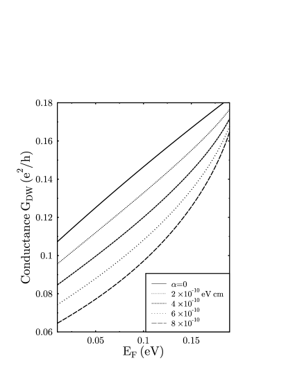
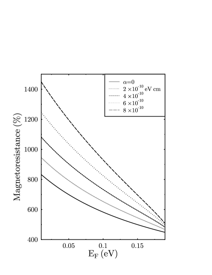
Figure 1 shows the calculated dependence of the electrical conductance on the Fermi-energy in the general case. The calculations were performed assuming the following values of the relevant parameters: (where is the free electron mass), eV, and cm. These parameters correspond to GaMnAs semiconductor, and satisfy the condition for eV.
We can estimate the magnitude of parameter by taking the value of the spin-orbit (SO) splitting , where the momentum is related to the density of carriers as . Assuming meV for cm-2 as a characteristic value for GaAs-GaAlAs heterostructures,pfeffer95 one obtains eVcm.
From Fig. 1 it is clear that the conductance increases monotonically with increasing because the barrier is felt smaller by electrons having higher energy. Furthermore, the conductance of a magnetic wire with DW diminishes with increasing strength of the spin-orbit interaction.
The dependence of the magnetoresistance on the Fermi energy is presented in Fig. 2 for different values of the parameter . The magnetoresistance is calculated with respect to the state without DW, , where is the resistance of the wire with DW and is its resistance in the absence of the wall (only spin-up channel is active). For our choice of parameters, the magnetoresistance is rather high and increases substantially with spin-orbit interaction.
The magnetoresistance measurements on magnetic semiconductors are usually performed at low temperatures because the corresponding Curie temperature is rather low. At such conditions, one can expect a significant contribution of the localization corrections to the conductivity. The role of the localization in the case of smooth DWs (for ) has been studied before, tatara97 ; lyanda98 and it was shown that the localization corrections are suppressed by an effective gauge field of the wall. This means that the contribution of the wall to resistance is negative, and the corresponding magnetoresistance is positive.
We have analyzed the role of localization corrections in the case of sharp DW. Qualitively, it can be described as the DW induced suppression of the quantum interference in triplet Cooperon channel.lee85 The singlet channel in ferromagnets is strongly suppressed by the internal magnetization.dugaev01 The suppression of the interference by DWs is related to dephasing of the wave function of electron transmitted through the barrier.jonkers99 ; tatara01 If the transmission through the wall is small, the corresponding dephasing length roughly equals to the distance of electron moving from a point (within the constriction) to the domain wall position (), and the dephasing time is , where is the diffusion coefficient. After averaging over of the localization correction , we find that the characteristic dephasing length is the constriction length itself, . In the case of sharp DWs, the localization correction diminishes the magnetoresistance due to the reflection from the wall, since it has a different sign.
IV Conclusions
We have presented a theoretical description of the resistance of a semiconducting magnetic nanojunction with a constrained DW in the case of a full spin polarization of electron gas. In the limit of , the electron transport across the wall was treated effectively as electron tunneling through a spin-dependent potential barrier. For such a narrow and constrained DW, the electron spin does not follow adiabatically the magnetization direction, but its orientation is rather fixed. However, DW produces some mixing of the spin channels. The spin-orbit interaction essentially enhances the magnetoresistance, whereas the localization corrections play the opposite role. However, the localization corrections can be totally suppressed by the spin-orbit interaction.dugaev01 This indicates that the spin-orbit interaction can play an important role and can lead to large enhancement of the magnetoresistance effect.
Acknowledgements.
This work is supported by Polish State Committee for Scientific Research under Grants Nos. PBZ/KBN/044/P03/2001 and 2 P03B 053 25, and also by INTAS Grant No. 00-0476.References
- (1) Email address: vdugaev@mpi-halle.de
- (2) A. D. Kent, J. Yu, U. Rüdiger, and S. S. P. Parkin, J. Phys. Cond. Matter 13, R461 (2001).
- (3) K. Hong and N. Giordano, J. Phys. Cond. Matter 13, L401 (1998).
- (4) U. Ruediger, J. Yu, S. Zhang, A. D. Kent, and S. S. P. Parkin, Phys. Rev. Lett. 80, 5639 (1998).
- (5) A. D. Kent, U. Rüdiger, J. Yu, L. Thomas, and S. S. P. Parkin, J. Appl. Phys. 85, 5243 (1999).
- (6) J. F. Gregg, W. Allen, K. Ounadjela, M. Viret, M. Hehn, S. M. Thompson, and J. M. D. Coey, Phys. Rev. Lett. 77, 1580 (1996).
- (7) N. Garcia, M. Muoz, and Y. W. Zhao, Phys. Rev. Lett. 82, 2923 (1999).
- (8) U. Ebels, A. Radulescu, Y. Henry, L. Piraux, and K. Ounadjela, Phys. Rev. Lett. 84, 983 (2000).
- (9) R. Danneau, P. Warin, J.P. Attané, I. Petej, C. Beigné, C. Fermon, O. Klein, A. Marty, F. Ott, Y. Samson, and M. Viret, Phys. Rev. Lett. 88, 157201 (2002).
- (10) H. D. Chopra and S. Z. Hua, Phys. Rev. B 66, 020403(R) (2002).
- (11) C. Rüster, T. Borzenko, C. Gould, G. Schmidt, L. W. Molenkamp, X. Liu, T. J. Wojtowicz, J. K. Furdyna, Z. G. Yu, and M. E. Flatté, Phys. Rev. Lett. 91, 216602 (2003).
- (12) P. Bruno, Phys. Rev. Lett. 83, 2425 (1999).
- (13) P. M. Levy and S. Zhang, Phys. Rev. Lett. 79, 5110 (1997).
- (14) R. P. van Gorkom, A. Brataas, and G. E. W. Bauer, Phys. Rev. Lett. 83, 4401 (1999).
- (15) G. G. Cabrera and L. M. Falicov, Phys. Status Solidi B 61, 539 (1974); 62, 217 (1974).
- (16) A. Brataas, G. Tatara, and G. E. W. Bauer, Phys. Rev. B 60, 3406 (1999).
- (17) V. K. Dugaev, J. Barnaś, A. Łusakowski, and Ł. A. Turski, Phys. Rev. B 65, 224419 (2002).
- (18) L. R. Tagirov, B. P. Vodopyanov, and K. B. Efetov, Phys. Rev. B 65, 214419 (2002); 63, 104428 (2001); L. R. Tagirov, B. P. Vodopyanov, and B. M. Garipov, J. Magn. Magn. Mater. 258-259, 61 (2003).
- (19) J. B. A. N. van Hoof, K. M. Schep, A. Brataas, G. E. W. Bauer, and P. J. Kelly, Phys. Rev. B 59, 138 (1999).
- (20) J. Kudrnovsky, V. Drchal, C. Blaas, P. Weinberger, I. Turek, and P. Bruno, Phys. Rev. B 62, 15084 (2000).
- (21) J. Kudrnovsky, V. Drchal, I. Turek, P. Streda, and P. Bruno, Surf. Sci. 482-485, 1107 (2001).
- (22) B. Yu. Yavorsky, I. Mertig, A. Ya. Perlov, A. N. Yaresko, and V. N. Antonov, Phys. Rev. B 66, 174422 (2002).
- (23) M. Ye. Zhuravlev, E. Y. Tsymbal, S. S. Jaswal, A. V. Vedyayev, and B. Dieni, Appl. Phys. Lett. 83, 3534 (2003).
- (24) V. K. Dugaev, J. Berakdar, and J. Barnaś, Phys. Rev. B 68, 104434 (2003).
- (25) M. E. Flatté and G. Vignale, Appl. Phys. Lett. 78, 1273 (2001).
- (26) C. Gould, C. Rüster, T. Jungwirth, E. Girgis, G. M. Schott, R. Giraud, K. Brunner, G. Schmidt, and L. W. Molenkamp, cond-mat/0407735.
- (27) P. Pfeffer and W. Zawadzki, Phys. Reb. B 52, R14332 (1995).
- (28) G. Tatara and H. Fukuyama, Phys. Rev. Lett. 78, 3773 (1997).
- (29) Y. Lyanda-Geller, I. L. Aleiner, and P. M. Goldbart, Phys. Rev. Lett. 81, 3215 (1998).
- (30) P. A. Lee and T. V. Ramakrishnan, Rev. Mod. Phys. 57, 287 (1985).
- (31) V. K. Dugaev, P. Bruno and J. Barnaś, Phys. Rev. B 64, 144423 (2001).
- (32) P. A. E. Jonkers, S. J. Pickering, H. De Raedt, and G. Tatara, Phys. Rev. B 60, 15970 (1999).
- (33) G. Tatara, Int. J. Mod. Phys. B 15, 321 (2001).