Surface and electronic structure of MOCVD-grown Ga0.92In0.08N investigated by UV and X-ray photoelectron spectroscopies
Abstract
The surface and electronic structure of MOCVD–grown layers of Ga0.92In0.08N have been investigated by means of photoemission. Stability of chemical composition of the surface subjected to Ar+ ion sputtering was proven by means of X-ray photoemission spectroscopy. The analysis of the relative intensities of In 3d, Ga 3p, and N 1s peaks showed that argon ion bombardment does not change significantly the relative contents of the layer constituents. Simultaneous efficient removal of the main contaminants (O and C) was observed during the sputtering procedure, proving that argon sputtering can be used as method for preparation of clean Ga1-xInxN surfaces.
For a clean (0001)-(1x1) surface prepared by repeated cycles of Ar+ ion sputtering and annealing, electronic structure was investigated. The band structure was explored along the -A direction of the Brillouin zone, measuring angle-resolved photoemission spectra along the surface normal. A similar set of data was also acquired for the same surface of GaN layer. Comparison of the collected data revealed an additional feature at the valence band edge, which can be ascribed to the presence of In in the layer.
1Institute of Physics, Polish Academy of Sciences, Aleja Lotników 32/46, PL-02 668 Warsaw, Poland
2Department of Physics, Chalmers University of Technology and Göteborg University, S-412 96 Göteborg, Sweden
3Facultés Universitaires Notre-Dame de la Paix, LISE, 61 rue de Bruxelles, B-5000 Namur, Belgium
4High Pressure Research Center, Polish Academy of Sciences, Sokolowska 29, PL-01 141 Warsaw, Poland
Keywords: Photoelectron spectroscopy (PES), X-ray photoelectron spectroscopy (XPS), Band structure, Nitrides
PACS 73.20.-r, 79.60.-i
1 Introduction
Epilayers of Ga1-xInxN are indispensable elements of optoelectronic devices operating within green-blue range of electromagnetic radiation spectrum [1, 2]. Introducing indium into the GaN matrix leads to a narrowing of the energy gap of the material from 3.5 to 1.9 eV and makes it possible to tune the energy of light emitted by the device. The perspective of promising applications together with interesting physical phenomena governing the radiative recombination efficiency have stimulated intensive investigations of this material. Detailed information about the electronic structure is important for both applications and research of elementary excitations in it. To get information about electronic band structure we must use experimental methods which enable direct probing of electronic states. Despite its surface sensitivity photoemission is widely accepted as one of the most suitable tools for such studies. However, atomically clean, ordered surfaces with unmodified chemical composition are a precondition for meaningful photoemission experiments. Since Ga1-xInxN is only available in the form of epitaxial layers grown by molecular beam epitaxy (MBE) or metal organic chemical vapor deposition (MOCVD), surfaces for photoemission studies cannot be obtained by cleavage under UHV conditions. Instead, UHV-compatible methods consisting in Ar+ ion sputtering and annealing have to be considered. They have been applied in various combinations in order to prepare surfaces of GaN epilayers for electronic structure studies [3, 4, 5, 6]. Such procedures led to clean, well ordered (0001)-(1x1) surfaces, suitable for band structure studies by means of angle-resolved photoelectron spectroscopy. However, it was found for indium containing nitride layers that the presence of In atoms modifies surface structure (for the (0001) orientation, particularly) [7], by formation of indium-rich surface nanostructures [8] or by inducing non-uniform depth distribution of constituent elements [9, 10]. Moreover, surface sputtering of multicomponent solid may lead to a substantial change in chemical composition of the subsurface layer. The extent of that effect has to be evaluated experimentally before studies of the band structure are undertaken. Due to such obstacles, experimental evidence concerning band structure of Ga1-xInxN is scarce, except of that referred to the edges of the bands forming the fundamental energy gap, which were obtained mainly by various optical measurements [11, 12, 13, 14, 15, 16, 17]. The bowing of band gap vs composition dependence in strained and relaxed layers of Ga1-xInxN was one of the main issues in those papers. Conclusions derived from the experiments were supported by theoretical calculations [13, 14, 18, 19, 20]. The density of states in the whole valence and conduction bands was investigated by soft X-ray emission and absorption [21]. Changes of the band structure as a function of indium content were reported, in particular for the top of the valence band, in the alloys with a degree of substitution lower than 0.1. The conclusions from that study will be taken into account in the analysis of our photoemission results. Some results of photoemission experiments on InN have also been reported [22].
In this paper, we report photoemission investigations of properties of MOCVD-grown Ga1-xInxN. The first part presents the X-ray photoelectron spectroscopy (XPS) study of this material subjected to Ar+ ion sputtering. This was aimed at revealing the effect of such surface treatment on chemical composition of the surface region of the sample in order to check if Ar+ sputter cleaning could be applied to surfaces intended for photoemission measurements. It has been proved here that such a procedure could be adequate for surface preparation of Ga1-xInxN before photoemission experiments.
The second part is devoted to the angle-resolved photoemission investigation of the band structure of Ga1-xInxN. The sample surface was prepared by Ar+ ion sputtering, followed by annealing at 600oC. Normal emission spectra acquired for photon energies from 26 to 76 eV enabled us to map the valence band structure along the -A direction of the Brillouin zone. The similar set of data was collected for the corresponding surface of a GaN layer thus enabling us to reveal an additional feature at the valence band edge of Ga1-xInxN. Comparison of our results with those derived from theoretical calculations of Ga1-xInxN valence band density of states [17] supports the assignment of the above feature to the presence of indium ions in the studied system.
2 Experimental
The investigated samples were prepared in the High Pressure Research Centre, Polish Academy of Sciences in Warsaw, Poland. The single crystalline layers of GaN and Ga1-xInxN (x = 0.08) were grown epitaxially by the MOCVD technique on the (0001) faces of bulk GaN crystals [23]. The substrate surface was covered with a 0.5 m thick buffer layer of GaN — subsequently, the layer of Ga0.92In0.08N with the thickness of 100 nm was grown. The whole structure was terminated by (0001) (Ga-polar) face. The lattice parameters (as determined by XRD) were c=5.157 A for GaN and c=5.253 A for Ga1-xInxN, with a=3.175 A for both materials. Bulk GaN crystals (the substrates) with hexagonal crystalline structure were grown by means of high pressure technique [24]. Their dislocation densities were as low as 10 - 100 cm-2 and they had no inversion domains on surfaces.
The influence of Ar+ bombardment on the Ga1-xInxN surface was studied by means of XPS. These experiments were performed using the photoemission spectrometer ESCA-300 at LISE FUNDP in Namur, Belgium. The base pressure in the system was p=110-10 Torr. The photoemission was excited by a monochromatized Al K X-ray beam (=1486.6 eV). The total energy resolution was about 0.35 eV. The sputtering was carried out under static Ar pressure of 510-7 hPa and 600 V acceleration potential.
The angle-resolved (AR) photoemission experiments were carried out at beamline 41 of the MAX-lab synchrotron radiation laboratory in Lund, Sweden. The overall energy resolution was kept around 150 meV, and the angular resolution was about 2o. The angle between incoming photon beam and the surface normal was kept at 45o. The surface crystallinity was assessed by low energy electron diffraction (LEED) which indicated a hexagonal (1x1) symmetry.
3 Results and discussion
3.1 Core level spectroscopy
X-ray photoemission spectroscopy was used for monitoring the process of surface cleaning of Ga1-xInxN epilayer, particularly, the changes of the chemical composition of the surface under sputtering. The core-level spectra of the Ga1-xInxN components (In 3d, Ga 3p, N 1s) and of the main surface contaminants (O 1s and C 1s) were acquired, after sequential sputtering steps. Fig. 1 shows the spectra of core levels of sample constituents. XPS binding energies were referenced to the C 1s peak of adventitious carbon at 284.8 eV [25].
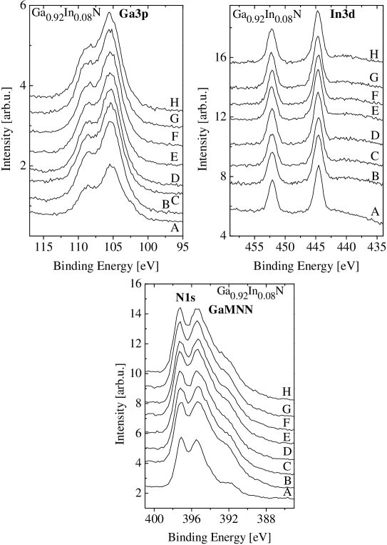
For In 3d and Ga 3p, the maxima are well discernible and spin–orbit splitting has been resolved. The N 1s peak partially overlaps the Auger GaMNN feature. The overall shape of these spectra did not change during sputtering. No appearance or disappearance of multiple components of the features could be discerned.
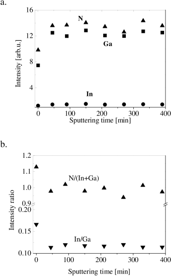
In order to evaluate possible changes in chemical composition of the surface and subsurface layer of the sample the peak intensities were determined as integrated area under the corresponding peaks. For N 1s, the area was measured under a single Gaussian extracted from the feature consisting of N 1s and GaMNN. The intensities were normalized to experimental conditions (number of scans, acquisition time etc.) and atomic sensitivity factors. For all three core levels we observed an increase of intensity after the first stage of sputtering (Fig. 2a). It was strongest for Ga 3d and relatively weak for In. Further sputtering did not lead to intensity changes, within the accuracy of our analysis. As a consequence, the intensity ratio In/Ga decreased from 0.17 (prior to sputtering) to the saturation level of 0.11 after 45 min. sputtering time (Fig. 2b). The latter value corresponds to the composition parameter x equal to 0.1 and remains reasonably consistent with its real value of 0.08. The observed change could be related to the reported non-uniform depth-compositional distribution in Ga1-xInxN layers grown by MOCVD [9, 10]. The N/(In+Ga) ratio also decreased after the first sputtering, most probably due to partial deficiency of nitrogen at the surface (induced by sputtering). Generally, this ratio is reasonably close to expected value of 1. A surface contribution of metal atoms, appearing due to sputtering, could easily be observed for Ga 3d at photon energies of 40-60 eV for [26] as well as (0001) surface. Such a component could not be discerned in the reported XPS spectra. It can be attributed to lower energy resolution and markedly higher electron escape depth for X-rays.
The measurement and analysis of the O 1s and C 1s spectra showed that Ar+ ion sputtering efficiently removes these elements from the sample surface. The most significant decrease of their content was observed after the first stage of sputtering (i.e. after 45 min. of Ar+ exposure). For the ”as mounted” surface, the O 1s feature could be decomposed into two maxima centered at 531.2 and 533.4 eV. According to Watkins et al. [27] the O 1s peak component at higher BE correspond to oxygen atoms adsorbed at the surface of GaN; the other one — to oxygen bound in the bulk of the crystal. We found that Ar+ ion cleaning leaves a trace amount of oxygen and carbon in the surface layer probed by XPS. This coincides with the results of Prabhakaran et al. [28] for surface of GaN. They attributed the residual C 1s emission to carbon atoms incorporated into the epilayer during its growth.
Concluding the analysis of cleaning the layer by Ar+ sputtering, one has to note that surface contaminants are removed efficiently and the energy positions of the core level peaks change toward lower BE due to removal of oxidized surface layer. However, the shape of Ga 3p, In 3d and N 1s peaks do not change during sputtering (no oxide-related components can be unequivocally revealed).
The surface morphology of the investigated samples was also studied by atomic force microscopy (AFM). A comparison of the patterns obtained before and after sputtering showed that such a process did not lead to marked destruction of the surface or to increase of its roughness. However, structures with step height of 1 or 1.5 nm and horizontal width of about 300 nm became discernible on the sputtered surface. The step height corresponds roughly to 2-3 lattice parameters along the c axis.
In conclusion we can state that Ar+ ion bombardment does not change the chemical composition of the surface and subsurface region of Ga1-xInxN layers markedly. Simultaneously, the sputtering provides significant reduction of oxygen and carbon concentration down to the level, where they do not influence the core–level spectra of Ga, In and N (see Figs. 1). Thus, X-ray photoemission spectroscopy shows that Ar+ ion bombardment can be used as a UHV-compatible method for preparation of clean Ga1-xInxN surfaces for photoemission experiments.
3.2 Angle-resolved photoelectron spectroscopy
Taking into account the results reported in the previous subsection we undertook an attempt to study band structure of Ga1-xInxN epitaxial layer cleaned in situ by multiple cycles of Ar+ ion sputtering and annealing at 600oC under UHV conditions. The most important aim of the study was assessment of In-related changes in the band structure of the solid solution. Therefore, parallel measurements were carried out for samples of Ga0.92In0.08N and GaN. The samples were fixed on the sample holder next to each other and cleaned together. So, the surface preparation, as well as the experimental conditions, were identical for both samples.
 |
 |
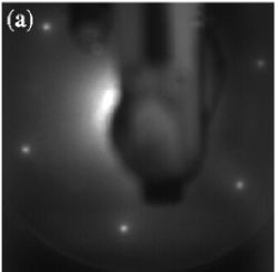
The crystallinity of the surfaces was checked using low energy electron diffraction (LEED) method. The LEED patterns indicated a hexagonal (1x1) symmetry of the surface for GaN as well as for Ga1-xInxN (Fig. 3). The surface composition of both samples was checked during the preparation process by spectroscopy of the Ga 3d level. Results of previous investigation concerning preparation of GaN(0001) (Ga-polar) surface by Ar+ ion bombardment and annealing showed that any changes in the surface conditions clearly manifested themselves in shape and position of Ga 3d structure. Sputtering efficiently removed oxidized Ga — it resulted in disappearance of relevant component of Ga 3d feature (observed for ”as grown” sample). Hence, after sputtering the Ga 3d feature was centered at the BE corresponding to pure gallium. Annealing of the sputtered sample resulted in decrease of the contribution related to pure gallium and appearance of the peak of Ga bound to N. These changes were clearly correlated with sharpening of the LEED pattern. Such a preparation procedure resulted in the clean, ordered GaN(0001)-(1x1) surface suitable for angle-resolved photoemission study [29]. Thus, the progress in the cleaning the surface during the sample treatment in this work was monitored by the observation of similar changes in the Ga 3d feature.
Angle-resolved photoemission was applied to study the electronic band structure along the -A direction in the Brillouin zone. Making use of synchrotron radiation we were able to measure the photoemission spectra for the energy range of 26-80 eV. Sets of normal emission spectra were acquired for Ga0.92In0.08N(0001)-(1x1) and for the corresponding surface of GaN (Fig. 4). A Shirley-type background was subtracted from the spectra. The origin of the BE scale has been adjusted to the valence band maximum (as determined for GaN from the experimental band structure diagram (Fig. 5)). The Fermi level position in the samples was around the edge of the conduction band, as estimated by photoemission measurement for a metallic reference sample in electric contact with investigated layers. This justifies excluding relation between features revealed at the valence band edge of Ga0.92In0.08N and appearance of any metal layer or islands on the sample surface.
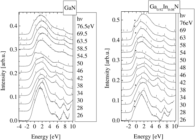
The overall shape of the spectra seems reasonably similar to those previously reported for GaN (0001) surfaces [4, 5, 30], taking into account differences between results obtained by various groups. Certain discrepancies should be attributed to modifications of surface preparation procedures. Irrespectively of differences in relative heights of the features, the spectra consist of two main groups of maxima. The first one, ranging from the valence band maximum to the BE of about 4 eV corresponds mainly to emission from the top valence bands. The second part of the curves is dominated by two features with weak dispersion (at BE of 5-6 eV and about 8 eV) and emission from the deeper valence band [31]. The corresponding spectra collected for GaN and Ga0.92In0.08N are generally similar. However, a clearly discernible feature appears at the leading edge of the spectra of In-containing layer for higher photon energies (58–76 eV). This feature overlaps with a weaker shoulder appearing for GaN at slightly higher binding energies. A similar, although weaker, modification can also be resolved for the spectra recorded for the lowest photon energies.
Two weak features could be revealed for the energies above the valence band maximum — at -2.0 and -3.4 eV for GaN, at -2.4 and -3.4 eV for Ga0.92In0.08N. It was shown by Wang et al. [34] that electronic states occur in the energy gap on the (0001)-(1x1) surface. However, it is difficult to relate our findings with the results of their calculation due to well known difficulty in determining of energy gap by DFT-LDA calculations. The energy position of the second feature coincides well with the width of GaN energy gap. The presence of such emission, although weak, may suggest strong band bending downwards and formation of an inversion layer at the surface of the samples. These features need and seem to deserve more detailed investigation.
In order to gain insight into details of the band structure of both systems the sets of photoemission spectra measured for normal emission were transformed into a band structure diagram along the -A direction (Fig. 5). Features appearing in the spectra were revealed and their energy positions were determined by means of an inverted second derivative method (marked with ticks and triangles in Fig. 4). Those BE values were used as the input data for calculation of corresponding k-vectors. We applied the free-electron final-state model using the formula:
| (1) |
The value for inner potential of the crystal V0=15.5 eV was determined by analysis of the curvature of the experimental bands and their correspondence to the available calculated band structure parameters of GaN. For almost all points, was equal to three basis vectors of the reciprocal lattice. In Fig. 5 points derived from the experimental data are marked with full and open symbols. The full lines have been drawn through the data points corresponding to the bulk bands (full dots) while dotted lines show the band structure calculated by Vogel et al. [32]. Dashed lines (drawn through open symbols) mark dispersionless features, possibly occurring due to emission from surface-related states or ”non-direct” emission from a high density–of–states parts of the bands.
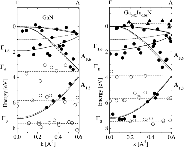
The width of the top part of the valence band (the energy separation between and ) is markedly larger in the experimental band structure than in the calculated one (about 1.9 and 1.0 eV, respectively). Similar discrepancy was previously observed for the surface of bulk GaN crystals [26], although the difference was smaller. The total width of the valence band at the point () is consistent with the results of calculations.
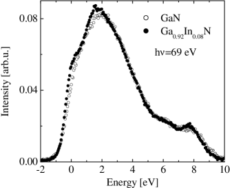
A comparison of the experimental band diagrams of both materials shows that the main modification of the band structure brought about by the admixture of In is an additional feature at the energy of 0.2 eV (marked with solid triangles). It led to an upward shift of the valence band edge of Ga0.92In0.08N. A similar effect was observed by X-ray absorption [21]. A shift of the valence band maximum by 0.15 eV was observed in N 2p soft x-ray emission spectra between GaN and Ga0.9In0.1N. Ryan et al. found it in agreement with results of empirical pseudopotential calculations of In wave functions and energy gap behavior in low-In content Ga1-xInxN. Bellaiche et al. [33] showed that the hole wave function localized around In could be interpreted as a combination of hybridized In functions with those of GaN valence band. Such a localization of states occurred above as well as below the valence band maximum of GaN. Our observation is also consistent with the results of first-principles calculations of band structure performed for GaN and Ga1-xInxN [17]. The calculations showed that some p states of nitrogen are pushed up from the top of the valence band, due to hybridization of In states and states of GaN. Thus, it seems to be justified to ascribe the dispersionless feature revealed in the Ga1-xInxN band structure to In(p,d)-N(p) hybridization states. It can easily be discerned in Fig. 6, where the differences between the spectra recorded for = 69 eV were visualized by direct comparison. The difference at the energy of 1.5 eV overlaps with bulk valence bands and cannot be discerned in the experimental band structure diagrams.
Dispersionless features discernible in the experimental band structures of GaN and Ga1-xInxN can be related to surface states or to non-direct emission from high density-of-states regions in the Brillouin zone. According to Wang et al. [34], a surface band occurs just below the lowest valence band. Its energy at the point is equal to 8 eV (with respect to the valence band maximum). Such a surface band is characteristic of the GaN(0001)-(1x1) surface terminated by additional layer of Ga atoms bound at positions. Emission from that state may contribute to the feature found at about 8 eV for both materials. However, one has to take into account the possibility of ”non-direct” emission from the lowest part of the valence band. Similarly, the feature at 4 eV can be connected with a surface band occurring around the point on a clean Ga-terminated (0001) surface, but again emission from high density of states region may be important. For the feature at 6 eV, we can consider a surface band between the K and M points of the surface Brillouin zone [34] and emission from bulk band at the K point.
4 Summary
The formation of Ga1-xInxN(0001) surface by Ar ion sputtering was investigated by X-ray photoelectron spectroscopy and atomic force microscopy. The intensities of the peaks related to emission from the Ga1-xInxN layer constituent elements (Ga, In, N) were measured for the sample ”as-mounted” and after subsequent stages of sputtering. For sputtering with Ar+ ions having relatively low kinetic energy (600 eV) no substantial modification of In/Ga ratio was observed, except for a weak change in chemical composition at the initial stage of sputtering. The main contaminants (oxygen and carbon) were efficiently removed from the surface. Therefore, we believe that argon ion sputtering can be used as a UHV-compatible method for preparation of clean Ga1-xInxN surfaces for photoemission experiments.
Comparative studies of the (0001)-(1x1) surfaces of Ga0.92In0.08N and GaN layers have been performed by angle-resolved photoemission in order to derive their band structure. The experimental band structures have been mapped along the -A direction of the Brillouin zone.
An additional dispersionless feature at the valence band maximum has been observed for Ga0.92In0.08N. The analysis based on comparison with available results of theoretical calculations enabled us to relate this feature to the states pushed up from the top of the valence band, due to hybridization of In and N states.
Acknowledgments This work was supported by KBN (Poland) project 2P03B 046 19 and by the European Commission - Access to Research Infrastructure action of the Improving Human Potential Programme (realized by MAX-lab facility in Lund). J.G. is supported by NFSR (Belgium) and F.M. by FRIA.
References
- [1] S. Nakamura, J. Vac. Technol. A 13 (1995) 705
- [2] S. Nakamura and G. Fasol The Blue Laser Diode (Springer, Berlin 1997)
- [3] R.W. Hunt, L. Vanzetti, T. Castro, K.M. Chen, L. Sorba, P.I. Cohen, W. Gladfelter, J.M. Van Hove, J.N. Kuznia, M. Asif Khan and A. Franciosi, Surf. Sci. 185 (1993) 415
- [4] S.A. Ding, S.R. Barman, K. Horn and V.L. Alperovich, Proc. 23rd Intern. Conf. Phys. Semicond. 1 (1996) 525
- [5] S.S. Dhesi, C.B. Stagarescu, K.E. Smith, D. Doppalapudi, R. Singh and T.D. Moustakas, Phys. Rev. B56 (1997) 10 271
- [6] R.A. Beach, E.C. Piquette and T.C. McGill, MRS Internet J. Nitride Semicond. Res. 4S1 (1999) G6.26
- [7] Huajie Chen, R.M. Feenstra, J.E. Northrup, T. Zywietz, J. Neugebauer and D.W. Greve, J. Vac. Sci. Technol. B18(4) (2000) 2284
- [8] Huajie Chen, R.M. Feenstra, J.E. Northrup, T. Zywietz and J. Neugebauer, Phys. Rev. Lett. 85 (2000) 1902
- [9] S. Pereira, M.R. Correia, E. Pereira, K.P. O’Donnell, C. Trager-Cowan, F. Sweeney and E. Alves, Phys. Rev. B64 (2001) 205311
- [10] S. Pereira, M.R. Correia, E. Pereira, K.P. O’Donnell, C. Trager-Cowan, F. Sweeney, E. Alves, A.D. Sequeira, N. Franco and I.M. Watson, phys. stat. sol (b) 228 (2001) 59
- [11] K. Osamura, S. Naka and Y. Murakami, J. Appl. Phys. 46 (1975) 3432
- [12] C. Wetzel, T. Takeuchi, S. Yamaguchi, H. Katoh, H. Amano and I. Akasaki, Appl. Phys. Lett. 73 (1998) 1994
- [13] M.D. McCluskey, C.G. Van de Walle, C.P. Master, L.T. Romano and N.M. Johnson, Appl. Phys. Lett. 72 (1998) 2725
- [14] C.G. Van de Walle, M.D. McCluskey, C.P. Master, L.T. Romano and N.M. Johnson Mat. Sci. Eng. B 59 (1999) 274
- [15] C.A. Parker, J.C. Roberts, S.M. Bedair, M.J. Reed, S.X. Liu, N.A. El-Masry and L.H. Robins, Appl. Phys. Lett. 75 (1999) 2566
- [16] K.P. O’Donnell, R.W. Martin, C. Trager-Cowan, M.E. White, K. Esona, C. Deatcher, P.G. Middleton, K. Jacobs, W. Van der Stricht, C. Merlet, B. Gil, A. Vantomme and J.F.W. Mosselmans, Mat. Sci. Eng. B 82 (2001) 194
- [17] P. Perlin, I. Gorczyca, T. Suski, P. Wisniewski, S. Lepkowski, N.E. Christensen, A. Svane, M. Hansen, S.P. DenBaars, B. Damilano, N. Grandjean and J. Massies, Phys. Rev. B64 (2001) 115319
- [18] A.F. Wright and J.S. Nelson, Appl. Phys. Lett. 66 (1995) 3051
- [19] S.K. Pugh, D.J. Dugdale, S. Brand and R.A. Abram J. Appl. Phys. 86 (1999) 3768
- [20] L.K. Teles, J. Furthmüller, L.M.R. Scolfaro, J.R. Leite and F. Bechstedt, Phys. Rev. B63 (2001) 085204
- [21] P. Ryan, C. McGuinness, J.E. Downes, K.E. Smith, D. Doppalapudi and T.D. Moustakas, Phys. Rev. B65 (2002) 205201
- [22] Q.X. Guo, M. Nishio, H. Ogawa, A. Wakahara and A. Yoshida, Phys. Rev. 58 (1998) 15 304
- [23] M. Leszczynski, P. Prystawko, R. Czernecki, J. Lehnert, T. Suski, P. Perlin, P. Wisniewski, I. Grzegory, G. Nowak, S. Porowski and M. Albrecht, J. Cryst. Growth 231 (2001) 352
- [24] I. Grzegory, J. Jun, M. Bockowski, S. Krukowski, M. Wróblewski, B. Lucznik and S. Porowski, J. Phys. Chem. Solids 56 (1995) 639
- [25] J.F. Moulder, W.F. Stickle, P.E. Sobol, K.D. Bomben, Handbook of X-ray Photoelectron Spectroscopy (Perkin-Elmer, Eden Prairie, MN, 1994)
- [26] B.J. Kowalski, R.J. Iwanowski, J. Sadowski, I.A. Kowalik, J. Kanski, I. Grzegory and S. Porowski, Surf. Sci. 548 (2004) 220
- [27] N.J. Watkins, G.W. Wicks and Gao Yongli, Appl. Phys. Lett. 75 (1999) 2602
- [28] K. Prabhakaran, T.G. Andersson and K. Nozawa, Appl. Phys. Lett. 69 (1996) 3212
- [29] L. Plucinski, T. Strasser, B.J. Kowalski, K. Rossnagel, T. Boetcher, S. Einfeldt, D. Hommel, I. Grzegory, S. Porowski, B.A. Orlowski, W. Schattke and R.L. Johnson, Surf. Sci. 507-510 (2002) 223
- [30] T. Maruyama, Y. Miyajima, S.H. Cho, K. Akimoto, H. Kato, Physica B 262 (1999) 240
- [31] T. Strasser, C. Solterbeck, F. Starrost and W. Schattke, Phys. Rev. B60 (1999) 11 577
- [32] D. Vogel, P. Krüger and J. Pollmann, Phys. Rev. B55 (1997) 12 836
- [33] L. Bellaiche, T. Mattila, L.W. Wang, S.-H. Wei and A. Zunger, Appl. Phys. Lett. 74 (1999) 1842
- [34] F.H. Wang, P. Krüger and J. Pollman, Phys. Rev. B64 (2001) 035305