[
Effect of impurities on transport through organic self-assembled molecular films from first principles
Abstract
We calculate electron transport through molecular monolayers of saturated alkanes with point defects from first principles. Single defects (incorporated Au ions, kinks, dangling bonds) produce deep localized levels in the gap between occupied and unoccupied molecular levels. Single defects produce steps on the I-V curve, whereas pairs of (unlike and like) defects give negative differential resistance peaks. The results are discussed in relation to the observed unusual transport behavior of organic monolayers and compared with transport through conjugated polythiophenes.
pacs:
PACS numbers: 85.65.+h] Recently, an interest towards the development and application of Langmuir-Blodgett films and self-assembled monolayers (SAM) has risen dramatically, which is in part related to widespread efforts in the area of molecular-size devices and sensors. At the same time, the fundamental understanding of these films is assessed as “very limited” [1]. Further, it has been concluded some decades ago that the conduction through absorbed [2] and Langmuir-Blodgett [3] monolayers of fatty acids (CH (we shall customarily refer to them as C) is associated with defects. In particular, Polymeropoulos and Sagiv have studied a variety of absorbed monolayers from C7 to C23 on Al/Al2O3 substrates and found that the exponential dependence on the length of the molecular chains is only observed below the liquid nitrogen temperature of 77K, and no discernible length dependence was observed at higher temperatures [2]. The current varied strongly with the temperature for LB films on Al/Al2O3 substrates in He atmosphere (believed to hinder the Al2O3 growth)[3], which is not compatible with elastic tunneling. The 100-fold increase of resistance of the annealed films was attributed to the “annealing” of “defects” with time. An absence of direct tunneling through self-assembled monolayers of C12-C18 has been reported by Boulas et al. [4]. On the other hand, an exponential dependence of monolayer resistance on the chain length , [5, 6] and no temperature dependence of the conductance in C8-C16 molecules was observed over the temperatures K, a signature of the elastic tunneling [6].
The electrons in alkane molecules are tightly bound to the C atoms by bonds, and the band gap (between the highest occupied molecular orbital, HOMO, and lowest unoccupied molecular orbital, LUMO) is large, eV [4], Fig. 1a. In conjugated systems with electrons the molecular orbitals are extended, and the HOMO-LUMO gap is correspondingly smaller, as in e.g. polythiophenes, where the resistance was also found to scale exponentially with the length of the chain, with Å-1 instead of Å-1[5]. In contrast with the temperature-independent tunneling results for SAMs [6], recent extensive studies of electron transport through 2.8 nm thick eicosanoic acid (C20) LB monolayers at temperatures 2K-300K have established that the current is practically temperature independent below K, but very strongly temperature dependent at higher temperatures K[7].
A large amount of effort went into characterizing the organic thin films and possible defects there [1, 8, 9]. It has been found that the electrode material, like gold, gets into the body of the film, leading to the possibility of metal ions existing in the film as single impurities and clusters. Electronic states on these impurity ions are available for the resonant tunneling of carriers in very thin films (or hopping in thicker films, a crossover between the regimes depending on the thickness). Depending on the density of the impurity states, with increasing film thickness the tunneling will be assisted by impurity “chains”, with an increasing number of equidistant impurities [10]. One-impurity channels produce steps on the I-V curve but no temperature dependence, whereas the inelastic tunneling through pairs of impurities at low temperatures defines the temperature dependence of the film conductance, and the voltage dependence of current [11]. This is a generic behavior observed in inorganic systems with defects[12, 13]. The tunneling may be accompanied by interaction with vibrons on the molecule, causing step-like features on the I-V curve [14, 15]. During processing, especially top electrode deposition, small clusters of the electrode material may form in the organic film, causing Coulomb blockade, which also can show up as steps on the I-V curve. It has long been known that a strong applied field can cause localized damage to thin films, presumably due to electromigration and the formation of conducting filaments[16]. Recent spatial mapping of the conductance in LB monolayers of fatic acids with the use of conducting AFM has revealed damage areas 30-100nm in diameter appearing after a “soft” electrical breakdown, sometimes accompanied by a strong temperature dependence of the conductance[17]. A crossover from tunneling at low temperatures to an activation-like dependence at higher temperatures is expected for electron transport through organic molecular films. There are recent reports about such a crossover in individual molecules like the 2nm long Tour wire with a small activation energy meV [18]. Our present results suggest that this may be a result of interplay between the drastic renormalization of the electronic structure of the molecule in contact with electrodes, and disorder in the film, illustrated by Fig. 2 (inset).
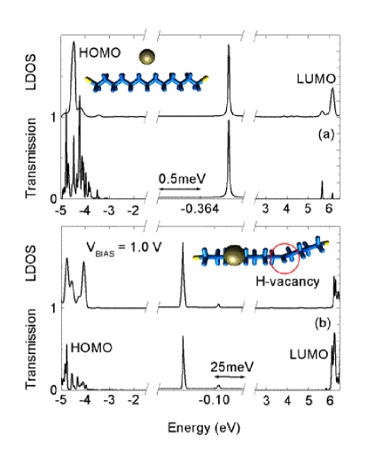
We report the ab-initio calculations of point-defect assisted tunneling through alkanedithiols S(CHS and thiophene T3 (three rings SC self-assembled on gold electrodes. The length of the alkane chain was in the range . We have studied single and double defects in the film: (i) single Au impurity, Figs. 1a, 2a, (ii) Au impurity and H vacancy (dangling bond) on the chain, Fig. 1b, 2c, (iii) a pair of Au impurities, Fig. 2b, (iv) Au and a “kink” on the chain (one C=C bond instead of a C-C bond). Single defect states result in steps on the associated I-V curve, whereas molecules in the presence of two defects generally exhibit a negative differential resistance (NDR). Both types of behavior are generic and may be relevant to some observed unusual transport characteristics of SAMs and LB films [2, 3, 7, 17, 18, 19].
We have used an ab-initio approach that combines the Keldysh non-equilibrium Green’s function (NEGF) method with self-consistent pseudopotential-based real space density functional theory (DFT) for systems with open boundary conditions provided by semi-infinite electrodes under external bias voltage [20, 21]. To construct the system Hamiltonian, we use self-consistent DFT within the local-density approximation. The atomic cores are defined using standard norm-conserving nonlocal pseudopotentials [22], and we expand the Kohn-Sham wave functions in a fireball [23] s-, p-, d- real-space atomic orbital basis[20]. We have checked that the results are reliable with respect to the size of the basis set. The Greens function is determined by direct matrix inversion. External bias is incorporated into the Hartree potential, and in this way the nonequilibrium charge density is iterated to self-consistency with imposed global charge neutrality, after which the current-voltage (I-V) characteristics have been computed. All present structures have been relaxed with the Gaussian98 code prior to transport calculations[24]. The conductance of the system at a given energy is found from
| (1) |
where is the retarded (advanced) Green’s function, is the self-energy part connecting left () and right () electrodes [20], and the current is found as
| (2) |
The equilibrium position of an Au impurity is about 3Å away from the alkane chain, which is a typical Van-der-Waals distance. Note that the conductance of alkanes is dominated by tunneling through the wide HOMO-LUMO gap (see below) and, therefore, is not sensitive to fine details of molecule-electrode coupling, unlike in the case of conjugated molecules, where the sensitivity to the geometry may be very high[25]. As the density maps show (Fig. 2), there is an appreciable hybridization between the s- and d-states of Au and the sp- states of the carbohydride chain. Furthermore, the Au ion produces a Coulomb center trapping a 6s electron state at an energy eV with respect to the Fermi level, almost in the middle of the HOMO-LUMO eV gap in Cn (DFT gaps are usually smaller than in experiment). The tunneling evanescent resonant state is a superposition of the HOMO and LUMO molecular orbitals. Those orbitals have a very complex spatial structure, reflected in an asymmetric line shape for the transmission. Since the impurity levels are very deep, they may be understood within the model of “short-range impurity potential” [26]. Indeed, the impurity wave function outside of the narrow well can be fairly approximated as
| (3) |
where , is the inverse radius of the state, where is the depth of the impurity level with respect to the LUMO, and =LUMO is the distance between the LUMO and the Fermi level of gold and, consequently, the radius of the impurity state is small. The energy distance is eV in alkane chains (CH[4] (eV from DFT calculations), and is the effective electron tunneling mass in alkanes[6]. For one impurity in a rectangular tunnel barrier [26] we obtain the Breit-Wigner form of conductance
| (4) |
where is the tunneling rate from impurity to the left (right) electrode, where is the tunneling amplitude from impurity to the electrode, is the electron band width in the electrodes. Using this model, we may estimate for an Au impurity in C13 (Å) the width , which is within an order of magnitude compared with the value eV calculated from (1). The transmission is maximal and equals unity when and which corresponds to a symmetrical position for the impurity with respect to the electrodes. The electronic structure of the alkane backbone, through which the electron tunnels to an electrode, shows up in the asymmetric lineshape, which is substantially non-Lorentzian, Fig. 1. The current remains small until the bias has aligned the impurity level with the Fermi level of the electrodes, resulting in a step in the current , (Fig.2a). This step can be observed only when the impurity level is not very far from the Fermi level such that biasing the contact can produce alignment before a breakdown of the device may occur.
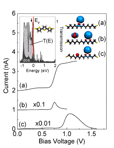
The most interesting situations that we have found relate to the pairs of point defects in the film. Indeed, some impurity levels on two sites may move in and out of resonance, see Eq.(6), and this obviously will lead to peaks on the I-V curve, or, equivalently, to Negative Differential Resistance (NDR). If the concentration of defects is , the relative number of configurations with pairs of impurities will be small, However, they give an exponentially larger contribution to the current. Indeed, the optimal position of two impurities is symmetrical, a distance apart, with current The conductance of a two-impurity chain is [26]
| (5) |
For a pair of impurities with slightly differing energies where is the distance between them. The interpretation of the two-impurity channel conductance (5) is fairly straightforward: if there were no coupling to the electrodes, i.e. the poles of would coincide with the bonding and antibonding levels of the two-impurity “molecule”. The coupling to the electrodes gives them a finite width and produces, generally, two peaks in conductance, whose relative positions in energy change with the bias. The same consideration is valid for longer chains too, and gives an intuitive picture of the formation of the impurity “band” of states. The maximal conductivity occurs when where is the width of the two-impurity resonance, and it corresponds to the symmetrical position of the impurities along the normal to the contacts separated by a distance equal to half of the molecule length, Under bias voltage the impurity levels shift as
| (6) |
where are the positions of the impurity atoms counted from the center of the molecule. Due to disorder in the film, under bias voltage the levels will be moving in and out of resonance, thus producing NDR peaks on the I-V curve. The most pronounced negative differential resistance is presented by a gold impurity next to a C chain with an H-vacancy on one site, Fig. 1b (the defect corresponds to a dangling bond). The defects result in two resonant peaks in transmission, Fig. 1b. Surprisingly, the H vacancy (dangling bond) has an energy very close to the electrode Fermi level , with eV (Fig. 1b, right peak in the middle). The relative positions of the resonant peaks move with an external bias and have crossed at 1.2V, producing a pronounced NDR peak in the I-V curve, Fig. 2c. No NDR peak is seen in the case of an Au impurity and a kink C=C on the chain because the energy of the kink level is far from that of the Au 6s impurity level. The calculated values of the peak current through the molecules were large: nA/molecule for an Au impurity with H vacancy, and nA/molecule for double Au impurities. We have observed a new mechanism for the NDR peak in a situation with two Au impurities in the film. Namely, Au ions produce two sets of deep impurity levels in C films, one stemming from the 6s orbital, another from the 5d shell, as clearly seen in Fig. 2b (inset). The 5d-states are separated in energy from 6s, so that now the tunneling through s-d pairs of states is allowed in addition to s-s tunneling. Since the 5d-states are at a lower energy than the s-state, the d- and s-states on different Au ions will be aligned at a certain bias. Due to the different angular character of those orbitals, the tunneling between the s-state on the first impurity and a d-state on another impurity will be described by the hopping integral analogous to the Slater-Koster integral. The peak current in that case is smaller than for the pair Au-H vacancy, where the overlap is of type (cf. Figs. 2b and 2c). Thiophene molecules behave very differently since the states there are conjugated and, consequently, the HOMO-LUMO gap is much narrower, just below 2 eV. The tail of the HOMO state in the T3 molecule (with three rings) has a significant presence near the electrode Fermi level, resulting in a practically “metallic” density of states and hence ohmic I-V characteristic. This behavior is quite robust and is in apparent disagreement with experiment, where the tunneling has been observed[5]. However, in actual thiophene devices the contact between the molecule and electrodes is obviously very poor, and it may lead to unusual current paths and temperature dependence[19].
We have presented the first parameter-free DFT calculations of a class of organic molecular chains incorporating single or double point defects. The results suggest that the present generic defects produce deep impurity levels in the film and cause a resonant tunneling of electrons through the film, strongly dependent on the type of defects. Thus, a missing hydrogen produces a level (dangling bond) with an energy very close to the Fermi level of the gold electrodes In the case of a single impurity, it produces steps on the I-V curve when one electrode’s Fermi level aligns with the impurity level under a certain bias voltage.
The two-defect case is much richer, since in this case we generally see a formation of the negative-differential resistance peaks. We found that the Au atom together with the hydrogen vacancy (dangling bond) produces the most pronounced NDR peak at a bias of 1.2V in C13. Other pairs of defects do not produce such spectacular NDR peaks. A short range impurity potential model reproduces the data very well, although the actual lineshape is different.
There is a remaining question of what may cause the strong temperature dependence of conductance in “simple” organic films like [CH. The activation-like conductance has been reported with a small activation energy meV in alkanes [7, 18] and even smaller, 10-100 meV, in polythiophenes [19]. This is much smaller than the value calculated here for alkanes and expected from electrical and optical measurements on C molecules, eV [4], which correspond nicely to the present results. In conjugated systems, however, there may be rather natural explanation of small activation energies. Indeed, the HOMO in T3 polythiophene on gold is dramatically broadened, shifted to higher energies and has a considerable weight at the Fermi level. The upward shift of the HOMO is just a consequence of the work function difference between gold and the molecule. In the presence of (inevitable) disorder in the film some of the electronic states on the molecules will be localized in the vicinity of . Those states will assist the thermally activated hopping of holes within a range of small activation energies eV. Similar behavior is expected for Tour wires[18], where eV[20](c), if the electrode-molecule contact is poor, as is expected. Metallic protrusions (filaments), emerging due to electromigration in a very strong electric field, and metallic, hydroxyl, etc. inclusions[16, 17] may result in a much smaller tunneling distance for the carriers and the image charge lowering of the barrier. The image charge lowering of the barrier in a gap of width is meaning that a decrease of about 3.5eV may only happen in an unrealistically narrow gap Å in a film with dielectric constant but it will add to the barrier lowering. More detailed characterization and theoretical studies along these lines may help to resolve this very unusual behavior. We note that such a mechanism cannot explain the crossover with temperature from tunneling to hopping reported for single molecular measurements, which has to be a property of the device, not a single molecule [18]. The work has been supported by DARPA.
REFERENCES
- [1] A. Ulman, Characterization of Organic Thin Films (Butterworth-Heinemann, Boston, 1995).
- [2] E.E. Polymeropoulos and J. Sagiv, J. Chem Phys. 69, 1836 (1978).
- [3] R.H. Tredgold and C.S. Winter, J. Phys.: Appl. Phys. D 14, L185 (1981).
- [4] C. Boulas et al., Phys. Rev. Lett. 76, 4797 (1996).
- [5] H. Sakaguchi et al. Appl. Phys. Lett. 79, 3708 (2001); X.D. Cui et al. Nanotechnology 13, 5 (2002).
- [6] W. Wang et al., Phys. Rev. B 68, 035416 (2003).
- [7] D.R. Stewart et al., to be published.
- [8] G.L. Fisher et al., J. Phys. Chem. B 104, 3267 (2000); K. Seshadri et al., Langmuir 15; 742 (1999).
- [9] A.V. Walker et al., J.Am.Chem.Soc. 126, 3954 (2004).
- [10] M. Pollak and J.J. Hauser, Phys. Rev. Lett. 31, 1304 (1973); I.M. Lifshitz and V.Ya. Kirpichenkov, Zh. Eksp. Teor. Fiz. 77, 989 (1979).
- [11] L.I. Glazman and K.A. Matveev, Sov. Phys. JETP 67, 1276 (1988).
- [12] Y. Xu, D. Ephron, and M.R. Beasley, Phys. Rev. B 52, 2843 (1995).
- [13] C.H. Shang et al., Phys. Rev. B 58, 2917 (1998).
- [14] N.B. Zhitenev, H. Meng, and Z. Bao, Phys. Rev. Lett. 88, 226801 (2002).
- [15] A.S. Alexandrov and A.M. Bratkovsky, Phys. Rev. B 67, 235312 (2003).
- [16] H. Carchano et al., Appl. Phys. Lett. 19, 414 (1971); N.R. Couch et al., Sol. St. Commun. 59, 7 (1986).
- [17] C.N. Lau et al., Nano Lett. 4, 569 (2004).
- [18] Y. Selzer et al., J. Am. Chem. Soc. 126, 4052 (2004).
- [19] N.B. Zhitenev, A. Erbe, and Z. Bao, Phys. Rev. Lett. 92, 186805 (2004).
- [20] J. Taylor, H. Guo and J. Wang, Phys. Rev. B 63, R121104 (2001); ibid. 63, 245407 (2001); J. Taylor et al., Phys. Rev. Lett., 89, 138301 (2002).
- [21] B. Larade and A.M. Bratkovsky, Phys. Rev. B 68, 235305 (2003); for more DFT transport studies see e.g. S. K. Nielsen et al, Phys. Rev. Lett. 89, 066804 (2002); M. Brandbyge et al., Phys. Rev. B 65, 165401 (2002); Y. Xue et al., Chem. Phys. 281, 151 (2002); A. Calzolari et al., Phys. Rev. B 69, 035108 (2004)
- [22] N. Troullier and J.L. Martins, Phys. Rev. B 43, 1993 (1991).
- [23] O.F. Sankey and D.J. Niklewski, Phys. Rev. B 40, 3979 (1989).
- [24] M. J. Frisch et al., GAUSSIAN98, Revision A.9, Gaussian, Inc., Pittsburgh, PA, 1998
- [25] A.M. Bratkovsky and P.E. Kornilovitch, Phys. Rev. B 67, 115307 (2003).
- [26] A.I. Larkin and K.A. Matveev, Zh. Eksp. Teor. Fiz. 93, 1030 (1987).