Ab initio study of reflectance anisotropy spectra of a sub-monolayer oxidized Si(100) surface
Abstract
The effects of oxygen adsorption on the reflectance anisotropy spectrum (RAS) of reconstructed Si(100):O surfaces at sub-monolayer coverage (first stages of oxidation) have been studied by an ab initio DFT-LDA scheme within a plane-wave, norm-conserving pseudopotential approach. Dangling bonds and the main features of the characteristic RAS of the clean Si(100) surface are mostly preserved after oxidation of 50% of the surface dimers, with some visible changes: a small red shift of the first peak, and the appearance of a distinct spectral structure at about 1.5 eV. The electronic transitions involved in the latter have been analyzed through state–by–state and layer–by–layer decompositions of the RAS. We suggest that new interplay between present theoretical results and reflectance anisotropy spectroscopy experiments could lead to further clarification of structural and kinetic details of the Si(100) oxidation process in the sub-monolayer range.
pacs:
78.68.+m, 71.15.Qe, 73.20.-r, 78.40.-qThe developments in the capability to monitor and to control oxidation of the silicon (100) surface at an atomic-scale resolution are a very important issue in semiconductor device technology. In fact, high quality gate insulators thinner than 2nm are today required, due to the continuous downscaling of the metal-oxide-semiconductor (MOS) devices (see, e.g., Ref. BaumvolSurfSci1999 ).
In the last two decades the adsorption of oxygen on silicon surfaces has been extensively studied, from both experimental and theoretical points of view. In particular, the effects induced by oxidation on the optical properties of the silicon surfaces are being thoroughly studied since the mid eighties SelloniPRB33_8885_1986 ; KeimSurfSci1987 . It has been known since then that O2 adsorption is dissociative, and that preferred final adsorption sites for O atoms are Si-Si bond-bridge positions. More recently, it has been shown that in the case of Si(100) the most favorable adsorption sites for O are the dimer-bridge, and the backbond site of the down atom of the surface dimer UchiyamaSurfSci1996 ; UchiyamaPRB53_7917_1996 . The latter site is slightly favored over the former when insertion of a single O atom is considered. When two oxygen atoms originated by the dissociation of an O2 molecule are present, then the most favorable configuration which can be reached in a barrierless or almost barrierless reaction (i.e. with oxygen present only on surface sites) is that with one oxygen inserted into the down atom backbond, and the other inserted into the dimer bond UchiyamaSurfSci433-435_896_1999 ; WidjayaJCP116_5774_2002 . It is in fact known that, during the first stages of oxidation, O2 adsorption and O migration to the dimer backbonds proceed as barrierless (or almost barrierless) reactions, as demonstrated by both experimental SREM1998 and theoretical works KatoPRL80_1998 ; KatoPRB62_15978_2000 . Configurations with oxygen moving deeper into the second and/or third layer have been theoretically predicted KageshimaPRL_81_5936_1998 , but require the overcoming of a non-negligible energy barrier and are not considered here. Further Si(100) oxidation has been shown to proceed in a layer-by-layer manner, giving rise to an oscillatory effect in the surface anisotropy, which has been detected by ”in situ” reflectance anisotropy spectroscopy measurements Yasuda2001 ; Matsudo-Yasuda2002 . The phenomenon of the growth of a SiO2 layer over the Si(100) surface, and the related problem of the properties of the Si-SiO2 interface, have received most of the attention, and several calculations of structural and electronic properties of the interface are available PasquarelloNature1998 ; xxxxAPL2000 . However, what happens in the very first stages of oxidation (below 1 ML coverage) is still poorly known: oxidation of the second layer starts soon NakayimaPRB63_113314_2001 , and recent experimental works Matsudo-Yasuda2002 ; Yasuda2003 do not focus on the formation of the first layer, which is completed in a very short time (less than 1 second) at the experimentally used O2 partial pressures 111The experimental conditions, with an O2 partial pressure as large as 10-2 Pa, lead an exposure at about 103 Langmuir in only a few seconds. As a consequence, the well-known surface originating negative RAS peaks at low energy disappear almost immediately (see figures 5 and 6 in reference Matsudo-Yasuda2002 ).. Since reflectance anisotropy spectroscopy is a very sensitive technique, which in the case of the clean Si(100) surface is able to detect small structural details ShiodaPRB57_R6823_1998 ; RossowManteseAspnesJvac1996 , and –in contrast with other characterization techniques based on electrons– can be used ”in situ” to monitor the process under manufacturing conditions, we suggest, with the present work, a possible application of reflectance anisotropy spectroscopy to shed light on the structural and kinetic details of the Si(100) oxidation process in the sub-monolayer range.
Our aim is to study in a detailed and quantitative way the changes on the RAS features induced by very low concentrations of chemisorbed oxygen on the Si(100) surface. To this scope, a layer-resolved analysis of the most relevant low-energy spectral features will be presented.
I Theory
The RAS is defined as the difference between the normalized reflectivities measured at normal incidence, for two orthogonal polarizations of light. Throughout this paper, the surface is perpendicular to the axis, and the direction is perpendicular to the Si-Si dimers of the reconstructed Si(100) surface. RAS is hence measured, as a function of the photon energy, as , where R is the (isotropic) Fresnel reflectivity. Describing the surface within a repeated slab geometry, one can express , () for normally incident light as manghi :
| (1) |
where is the polarization direction, are the diagonal terms of the half-slab polarizability tensor, and is the complex bulk dielectric function.
If the slab has a center of inversion or a mirror plane parallel to the surface ( symmetry, in our case), the imaginary part of can be written, in the single–quasiparticle approximation, as:
| (2) |
where are the matrix element of the velocity operator between occupied () and empty () slab eigenstates at the point in the surface Brillouin zone delsole1 . ”A” is the slab surface area, while and are conduction and valence energy eigenvalues, taken as representative of quasiparticle energies. Neglecting the pseudopotential nonlocality noi_nonloc , the velocity operator can be replaced by the momentum operator divided by the electronic mass, whose matrix elements are easy to evaluate in the plane-wave basis. If the slab has two identical surfaces, is simply obtained by dividing by two the polarizability of the full slab. There are many cases, however, where one needs to single out the contributions coming from an individual half of the slab, or from regions situated at different depths below the surface. This problem has been recently discussed by some of us hogan and by others bechstedt ; monachesi , and can be solved by introducing a real-space cutoff in the definition of the matrix elements.
This method proved itself very useful for separating surface contributions from bulk and subsurface ones in optical spectra, and has already been applied to the case of the clean Si(100) reconstructed surface hogan . In the real-space cutoff scheme, modified matrix elements are needed, which incorporate a function switching from 1 inside the selected region to zero outside the selected region. are defined as:
| (3) |
The imaginary part of the polarizability is hence given by hogan :
| (4) |
where both and (the standard momentum matrix element, calculated without the cut-off function) appear. Working in the reciprocal space, the evaluation of requires a double sum over the reciprocal lattice vectors {}, in contrast to the single sum which yields hogan , 222Because of the double sum, the computation of the matrix elements using the cutoff technique can become time consuming, especially when a high cutoff energy is required for convergence. We have checked convergence of the matrix elements calculation over the number of –vectors included in the sum. We have obtained that 4000 -vectors are enough for achieving convergence, approximatively 1/5 of the initial basis size..
II computational details
Electronic wavefunctions and eigenvalues are obtained within the local density approximation (LDA) to density-functional theory hohenberg ; sham using a plane-waves basis set. The exchange-correlation energy is evaluated according to the Ceperley and Alder results alder as parametrized by Perdew and Zunger perdew . The ion-electron interaction is represented by norm-conserving pseudopotentials. Special attention was devoted to the generation of a good norm-conserving pseudopotential for oxygen, in order to achieve an high transferability without requiring too many plane waves for convergence. To this aim, we adopted the Hamann scheme hamann , and optimized the core radii in order to find the best compromise between the basis set convergence and transferability. The latter was checked not only against logarithmic derivatives, but also performing explicit atomic calculations in several excited configurations. More extensive pseudopotential tests have been performed on three small molecules (SiO, H2SiO, Si2O) and on the -quartz crystalline phase of silica, in order to check the convergence of their structural and electronic properties with respect to the basis set (number of plane waves). As a result, the theoretical length of the Si-O bond is found to converge (within 1%) already at a 30 Ry cutoff for all three molecules. The theoretical values of 1.51 Å (SiO) and 1.52 Å (H2SiO) compare well with the experimental ones (1.51 Å vecchia_referenza_17 and 1.515 Å silanone1 respectively). Concerning -quartz, the calculated lattice constant at 30 Ry is 4.87 Å, to be compared with the experimental value of 4.916 Å expt_alpha_quartz .
The Si(100) surface was simulated by a repeated slab of twelve silicon layers and four layers of vacuum. The surface unit cell has been choosen as a (2x2) one, for computational convenience, in order to be able to consider both the (2x1) and p(2x2) reconstructions within the same cell. First, the clean surface structure has been determined by a full structural optimization (keeping only the central four Si layers as fixed), using the Broyden-Fletcher-Goldfarb-Shanno minimization algorithm as implemented in the ABINIT code abinit until the residual forces acting on each atom are less than 0.01 eV/Å. The resulting structure was p(2x2) reconstructed in agreement with previous results RamstadPRB_51_14504_1995 , with a dimer buckling of 0.79 Å. The ground state of the c(4x2) reconstruction, requiring a different surface unit cell, has also been considered for comparison.
From the structural point of view, the difference between c(4x2) and p(2x2) is very tiny: in both cases one has rows of buckled Si dimers, and the buckling (at difference with the (2x1) reconstruction) alternates along those rows. The only difference between c(4x2) and p(2x2) consists in the buckling alternance in the direction perpendicular to the rows.
Considering that, as shown in Ref. palummosi100 , the dimer-dimer interaction is much larger along the rows than between adjacent rows very small energetic and spectral differences between c(4x2) and p(2x2) are to be expected. In fact, from the theoretical point of view, the stabilities of the p(2x2) and c(4x2) reconstructions are essentially identical RamstadPRB_51_14504_1995 . Recently, ab initio calculations have shown that it is possible to induce the formation of p(2x2) domains by electric fields or charge injection SeinoPRL_93_036101_2004 .
Experimentally, the coexistence of p(2x2) and c(4x2) domains at very low temperature is supported by recent low-temperature non contact atomic force microscopy data, which show that almost 12 % of the ordered Si(100) surface is p(2x2) reconstructed UozumiSurfSci_188_279_2002 . Hence, the p(2x2) cell can be taken as a realistic model of the clean Si(100) surface.
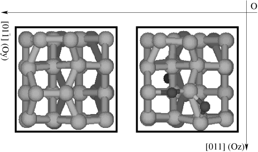
Two O atoms were then adsorbed on each of the two slab surfaces (in order to preserve the inversion symmetry), which corresponds to a 0.5 ML oxidation. Based on previous ab initio calculations of oxygen adsorption on the Si(100) surface UchiyamaSurfSci433-435_896_1999 ; WidjayaJCP116_5774_2002 , we have chosen the most stable configuration that can be reached in a barrierless or almost barrierless dissociation of the molecule: one O atom is in bridge position on a surface Si-Si dimer, and the second O atom also in bridge position on a nearest Si-Si backbond. Many previous theoretical results UchiyamaSurfSci1996 ; UchiyamaPRB53_7917_1996 ; KatoPRL80_1998 have shown that: i) the preferred adsorption site of an isolated O atom is a Si-Si backbond; ii) the backbond of the ”down atom” of the dimer is strongly preferred over the ”up atom” backbond (at the point that if adsorption occurs on the backbond of the ”up atom”, this is sufficient to induce locally the reversing of the buckling); iii) when an O2 molecule adsorbs, it dissociates leaving KatoPRB62_15978_2000 one oxygen atom into the Si-Si surface dimer bond, and the remaining atom into the ”down atom” backbond. We consider hence the configuration denoted by (h) in Ref. WidjayaJCP116_5774_2002 . The same structure is also considered (denoted by ”A”) in Fig. 1 (a) of Ref. KageshimaPRL_81_5936_1998 . This structure has been selected among the several other total energy minima for two oxygen atoms on Si(100), because it can be immediately reached after O2 dissociation (at difference with structures ”D” and ”E” of Ref. KageshimaPRL_81_5936_1998 ) and can efficiently model the effects of ”breaking” one of the surface Si-Si dimers.
III Results
After oxygen adsorption on the dimer and backbond bridge sites (Fig. 1), and a new full structural relaxation, one of the surface Si-Si dimers is broken (see Tab. 1: the dimer length after oxidation becomes 3.06 Å). Concerning the length of the oxidized Si backbond, we obtain 2.53 Å after O adsorption, to be compared with the 2.60 Å reported in Ref. UchiyamaSurfSci1996 . The structural relaxation remains limited to the immediate neighbouring of the O atom, since subsurface layers (2nd and 3rd silicon layer) are not affected appreciably. The buckling of the non-oxidized dimer, which is expected to be stabilized by O adsorption UchiyamaPRB53_7917_1996 , increases only very slightly, passing from 0.79 to 0.81 Å.
To compute optical spectra, the ground state calculation must be followed by a calculation of bandstructure energies and wavefunctions over a dense mesh in the irreducible wedge of the Brillouin zone, for both occupied and empty states. To this aim, we calculated Kohn–Sham eigenvectors and eigenvalues using the Arnoldi algorithm arnoldi , for all states up to 12 eV above the highest occupied state (i.e., about 250 empty states above the 108 filled ones) in each –point.
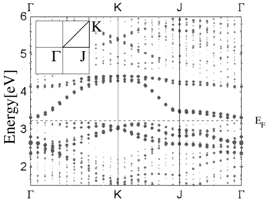
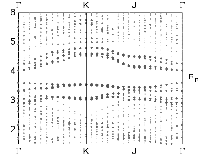
Fig. 2 shows the computed bandstructure, near the Fermi level, for both the clean and the oxidized surfaces, along the path in the irreducible wedge of the surface Brillouin zone. For the clean surface, results are in excellent agreement with previous ab initio DFT-LDA calculations RamstadPRB_51_14504_1995 on the Si(100)–p(2x2) surface. We note the strong dispersion along and for the surface bands arising from the dangling bonds which form (bonding) and (antibonding) states. This large dispersion is associated with a non-negligible interaction between adjacent silicon dimers in the direction perpendicular to the dimer axis palummosi100 ; kress (this is the direction along which the p(2x2) and c(4x2) surfaces are identical).
After oxidation, the direct gap at increases from 0.2 to 0.4 eV. However, surface states are still localized on DBs, as can be seen from a plot (not shown) of their charge densities. Even the oxidized dimers show distinct filled and empty DB-like surface states. The band dispersion in the direction perpendicular to dimers becomes smaller, which can be explained by a weakening of the interaction between adjacent dimers (in our case, an oxidized and a non oxidized one), as a consequence of oxidation. Oxidation also lifts the initial degeneracy of surface bands at the corner of the surface Brillouin zone.
Optical spectra have been computed according to Eq. (4), using increasingly large sets of –points (up to 162). The following Monkhorst–Pack monkhorst , –point meshes were considered in the upper half of the (2x2) Surface Brillouin Zone: 5x5, 7x7, 9x9, 11x11 and 18x9. In the energy window 0-3.5 eV, the 9x9 mesh is sufficient to achieve convergence, superimposing a small Gaussian broadening (75 meV) to the calculated spectrum. Similarly, in the range between 6 and 12 eV, the 11x11 mesh is sufficient, with the same small broadening. The intermediate energy window, between 3.5 and 6 eV, is the most slowly convergent one. Indeed, a fully converged RAS in this region can only be obtained by increasing the broadening up to 250 meV, with the largest –point sets used (11x11 and 18x9). These results are summarized in Fig. 3. In the right panel, the lowest-exposure experimental data from reference Yasuda2001 are also reported for comparison.
Comparing the RAS of the oxidized and clean surfaces up to 1.8 eV two differences come into evidence: i) after oxygen adsorption, there is a redshift by 0.2 eV of the main transition peak of the clean surface, and ii) a new structure appears between 1.4 and 1.75 eV (see Fig. 4). However, the overall RAS lineshape does not undergo qualitative changes. In the inset we also plot the RAS of the clean Si(100)–c(4x2) reconstruction, which below 1.6 eV is practically identical to that of p(2x2) 333The slight differences between the present results and those of Ref. palummosi100 are due to a present better convergence in the -points sampling..
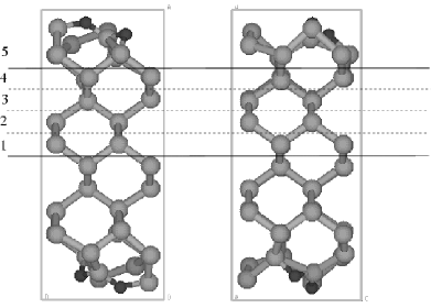
In order to clarify the origin and nature of oxygen-induced modifications, we have performed a layer-by-layer analysis of the RAS according to Eq. (3) and Eq. (4), applying the real-space cutoff method described in Ref. hogan . This allows one to quantify the contribution to the RAS originated in the different surface and subsurface regions. We divided our slab in five slices: the first four (starting from the middle of the slab) containing only silicon atoms, and the last one including surface dimers, oxygen atoms, and the subsurface Si atoms bonded to the surface dimers, as shown in Fig. 5. For the last slice, the cutoff region extends up to a distance of about 1 Å above the surface. The resulting spectra are displayed in Fig. 6: as expected, the reflectance anisotropy signal coming from slice 1 and slice 2 is almost zero up to 3.0 eV (i.e., in the whole region below the bulk Si direct gap), coherently with the fact that they are bulk representative. The presence of the surface starts to be felt in the 3rd slice, where the two main negative RAS peaks, characteristic of the clean surface, start to appear (at about 1 and 3 eV, respectively). Slice 4 gives a contribution very similar to slice 3, with a larger strength of the 1.0 eV peak. The latter peak is also strongly present in the topmost slice contribution, together with the 3 eV one. An analysis of the localization of electronic states involved in strongest dipole allowed transitions for the 1.0 eV peak show almost no contributions from electronic states involving O atoms. Indeed, the states which originate this peak are valence states corresponding mainly to dangling bonds localized on the upper Si atom of the oxidized dimer, and conduction states corresponding mainly to -like orbitals of the lower silicon atom of the non-oxidized dimer. However, besides the two main peaks at 1 and 3 eV, the topmost slice also contributes with a new structure, located at about 1.5 eV, which does not appear in slice 3 and slice 4 contributions. Empty states involved in the transitions responsible for this feature are in fact found to be strongly localized on the lower Si atom of the Si-O-Si bridge (broken dimer), and on the O atoms themselves (-like orbitals), so this feature represents a sort of oxygen signature.
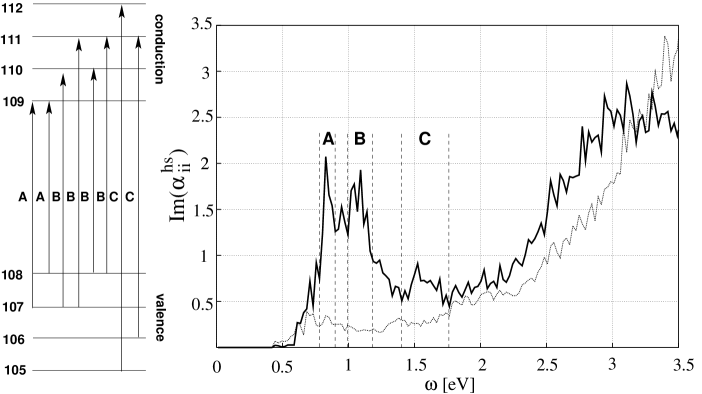
In order to obtain deeper insight on the electronic states involved in the main spectral structures, we have singled out, from the whole summation appearing in Eq. (4), the contributions which give the largest oscillator strength and the larger anisotropy, restricted to well-defined energy windows centered on the main low-energy peaks of the imaginary part of the slab polarizability tensor. To this aim, we have selected three energy windows, labeled with A, B and C (Fig. 7). based on the plot of the imaginary part of the half-slab polarizability for light polarization perpendicular () and parallel () to the silicon dimers. In each region, the contribution coming from each –point and band pairs () have been sorted on the basis of two criteria: the value of the squared modulus , and the value of the anisotropy calculated as . As a result, only the uppermost 4 valence states (labeled: 105–108) and the lowest 4 conduction states (labeled: 109–112) are found to be the main responsibles for the strongest optical transitions, with 107 109 and 108 109 contributing to peak A ([0.8,0.9] eV), and 107+108 110+111 contributing to peak B ([1.0,1.15] eV), while peak C ([1.40,1.75] eV) is due to the transitions 106 111 and 105 112, as illustrated in Fig. 7.
This result is confirmed by the comparison of the full RAS with a spectrum computed including only this set of 4 valence and 4 conduction states (i.e., based on just 16 out of 27216 - transitions): in the energy window between 0 and 1.8 eV all main features of the RAS are reproduced, apart for small difference in intensities (Fig. 8).
IV CONCLUSIONS
In conclusion, we have studied the very first stage of oxidation of Si(100)–p(2x2), at a coverage of 0.5 ML, showing that oxidation of one of the two Si–Si dimers of the p(2x2) unit cell does not change dramatically the RAS shape, despite the breaking of the dimer and the large flattening of the lowest conduction band, which reflects the weakening of the dimer–dimer interaction along the direction perpendicular to the dimer axis. In particular, the negative peak at 3.7 eV does not disappear (see footnote 42). However, oxidation of one dimer gives rise to distinguishable effects on the RAS in the lowest energy region (0 to 1.8 eV), which can be understood in terms of transitions between the four highest valence bands and the four lowest conduction bands of the slab, localized essentially on dangling bonds of silicon atoms, belonging to both types of dimers (oxidized and non-oxidized). These effects are essentially summarized by a redshift of about 0.2 eV of the first RAS negative peak, disappearance of the small structures below 1.0 eV, typical of the clean surface, and appearance of a new structure at 1.5 eV, which can be seen as an ”oxygen signature”. The latter can be clearly separated from extra artificial oscillations induced by the discreteness of the Brillouin zone sampling, when a sufficiently large number of –points is used. The shift of the first negative peak is strongly linked to the structural surface relaxation which follows oxygen adsorption, and becomes larger if the relaxation is not complete. A layer-by-layer analysis of the RAS shows that the 1.5 eV structure is extremely surface–localized (topmost 2.64 Å), while the origin of the two main negative peaks also extends somehow to the subsurface region (topmost 5.42 Å). We predict that the appearance of this feature should be detectable in reflectance anisotropy spectroscopy experiments on Si(100) in the sub-monolayer range. Our theoretical predictions could be experimentally assessed by reducing the oxygen exposure to a value of the order of 1-10 Langmuir, to be compared with the 103 Langmuir of presently available exprimental data.
V ACKNOWLEDGEMENTS
We acknowledge the European Community for financial support under the NANOQUANTA project (contract no. NMP4-CT-2004-500198), and the Italian “Ministero dell’Istruzione, dell Università e della Ricerca” for financial support within COFIN 2002. A. Incze also acknowledges support through the EEC under contract no. HPRNT-CT-2000-00167 (Univ. Tor Vergata, Roma). We would like to thank C. Hogan, M. Palummo, and M. Gatti for useful discussions, and N. Manini for a careful reading of the manuscript. Computer facilities at CINECA granted by INFM (Project ID n. 239488704824) are gratefully acknowledged.
References
- (1) I. J. R. Baumvol, Surf. Sci. Rep. 36, 1 (1999).
- (2) A. Selloni, P. Marsella, and R. Del Sole, Phys. Rev. B 33, 8885 (1986).
- (3) E. G. Keim, L. Wolterbeek, and A. van Silfhout, Surf. Sci. 180, 565 (1987).
- (4) T. Uchiyama and M. Tsukada, Surf. Sci. 357, 509 (1996).
- (5) T. Uchiyama and M. Tsukada, Phys. Rev. B 53, 7917 (1996).
- (6) T. Uchiyama, T. Uda, and K. Terakura, Surf. Sci. 433, 896 (1999).
- (7) Y. Widjaja and C. B. Musgrave, J. Chem. Phys. 116, 5774 (2002).
- (8) H. Watanabe, K. Kato, T. Uda, K. Fujita, M. Ichikawa, T. Kawamura, and K. Terakura, Phys. Rev. Lett. 80, 345 (1998).
- (9) K. Kato, T. Uda, and K. Terakura, Phys. Rev. Lett. 80, 2000 (1998).
- (10) K. Kato and T. Uda, Phys. Rev. B 62, 15978 (2000).
- (11) H. Kageshima and K. Shiraishi, Phys. Rev. Lett., 81, 5936 (1998).
- (12) T. Yasuda, S. Yamasaki, M. Nishizawa, N. Miyata, A. Shklyaev, M. Ichikawa, T. Matsudo, and T. Ohta, Phys. Rev. Lett. 87, 037403 (2001).
- (13) T. Matsudo, T. Ohta, T. Yasuda, M. Nishizawa, N. Miyata, S. Yamasaki, A. A. Shklyaev, and M. Ichikawa, J. of Appl. Phys. 91, 3637 (2002).
- (14) A. Pasquarello, M. S. Hybertsen, and R. Car, Nature 396, 58 (1998).
- (15) T. Nakayama and M. Murayama, Appl. Phys. Lett. 77, 4286 (2000).
- (16) K. Nakajima, Y. Okazaki, and K. Kimura, Phys. Rev. B 63, 113314 (2001).
- (17) T. Yasuda, N. Kumagai, M. Nishizawa, S. Yamasaki, H. Oheda, and K. Yamabe, Phys. Rev. B 67, 195338 (2003).
- (18) R. Shioda and J. van der Weide, Phys. Rev. B 57, R6823 (1998).
- (19) U. Rossow, L. Mantese, and D. E. Aspnes, J. Vac. Sci. Technol. B 14, 3070 (1996).
- (20) F. Manghi, R. Del Sole, A. Selloni, and E. Molinari, Phys. Rev. B 41, 9935 (1990).
- (21) R. Del Sole, Reflectance Spectroscopy-Theory, in Photonic Probes of Surfaces, edited by P. Halevi, (Elsevier, Amsterdam 1995), p.131.
- (22) see e.g.: A. Marini, G. Onida, and R. Del Sole, Phys. Rev. B 64, 195125 (2001).
- (23) C. Hogan, R. Del Sole, and G. Onida, Phys. Rev. B 68, 035405 (2003).
- (24) C. Castillo, B. S. Mendoza, W. G. Schmidt, P. H. Hahn, and F. Bechstedt, Phys. Rev. B 68, 041310(R) (2003).
- (25) P. Monachesi, M. Palummo, R. Del Sole, A. Grechnev, and O. Eriksson, Phys. Rev. B 68, 035426 (2003).
- (26) P. Hohenberg and W. Kohn, Phys. Rev. 136, B864 (1964).
- (27) W. Kohn and L.J. Sham, Phys. Rev. 140, A1133 (1965).
- (28) D. M. Ceperley and B. J. Alder, Phys. Rev. Lett. 45, 566 (1980).
- (29) J. P. Perdew and A. Zunger, Phys. Rev. B 23, 5048 (1981).
- (30) G. B. Bachelet, D. R. Hamann, and M. Schlüter, Phys. Rev. B 26, 4199 (1982).
- (31) Molecular spectra and molecular structure, by G. Herzberg, 2nd edition, New York, Van Nostrand Reinhold, (1950).
- (32) M. Bogey, B. Delcroix, A. Walters, and J.-C. Guillemin, J. Mol. Spectrosc. 175, 421 (1996).
- (33) L. Levien, C.T. Prewitt, and D. J. Weidner, Am. Mineral. 65, 920 (1980).
- (34) X. Gonze, J.-M. Beuken, R. Caracas, F. Detraux, M. Fuchs, G.-M. Rignanese, L. Sindic, M. Verstraete, G. Zerah, F. Jollet, M. Torrent, A. Roy, M. Mikami, Ph. Ghosez, J.-Y. Raty, and D.C. Allan, Comput. Mat. Sci. 25, 478 (2002).
- (35) A. Ramstad, G. Brocks, and P. J. Kelly, Phys. Rev. B 51, 14504 (1995).
- (36) M. Palummo, G. Onida, R. Del Sole, and B. S. Mendoza, Phys. Rev. B 60, 2522 (1999).
- (37) K. Seino, W.G. Schmidt, and F. Bechstedt, Phys. Rev. Lett. 93, 036101 (2004).
- (38) T. Uozumi, Y. Tomiyoshi, N. Suehira, Y. Sugawara, S. Morita, Appl. Surf. Sci., 188, 279 (2002).
- (39) ARPACK Users’ Guide: Solution of Large-Scale Eigenvalue Problems with Implicitly Restarted Arnoldi Methods, by R. B. Lehoucq, D. C. Sorensen, and C. Yang, edited by SIAM, Philadelphia, (1998). ARPACK-Arnoldi Package, www.caam.rice.edu/software/ARPACK.
- (40) C. Kress, A. Shkrebtii, and R. Del Sole, Surf. Sci. 377, 398 (1997).
- (41) J. D. Pack and H. J. Monkhorst, Phys. Rev. B 16, 1748 (1977).
| surface | (Å) | (Å) | ||
|---|---|---|---|---|
| clean | 19.2 | 2.33 | 19.2 | 2.33 |
| oxidized | 11 | 3.06 | 20.27 | 2.34 |
| (-43%) | (+31%) | (+6%) | (0.4%) |
|
|
|---|---|
| wavevector | wavevector |

|

|