Optical response for the d-density wave model
Abstract
We have calculated the optical conductivity and the Raman response for the d-density wave model, proposed as a possible explanation for the pseudogap seen in high cuprates. The total optical spectral weight remains approximately constant on opening of the pseudogap at fixed temperature. This occurs because there is a transfer of weight from the Drude peak to interband transitions across the pseudogap. The interband peak in the optical conductivity is prominent but becomes progressively reduced with increasing temperature, with impurity scattering, which distributes it over a larger energy range, and with inelastic scattering which can also shift its position, making it difficult to have a direct determination of the value of the pseudogap. Corresponding structure is seen in the optical scattering rate, but not necessarily at the same energies as in the conductivity.
pacs:
71.10.-w,74.72.-h,78.20.BhI Introduction
The pseudogap in the cuprates is widely believed to hold an important clue to the fundamental nature of these systems.timuskpseudo Through angular resolved photoemission studiesding ; shen of the variation around the Fermi surface of the leading edge of the electron spectral density, it has been established that the pseudogap has d-wave symmetry as does the superconducting gap. A smooth evolution of the superconducting gap into the pseudogap is also observed in tunnelingrenner which shows that, in the underdoped regime, the gap fills in with increasing temperature but does not close as one goes through . These ideas have led to a school of thought that believes that the pseudogap is a precursor to superconductivity. One model is the preformed pairkivelson ; emery model with phase coherence lost at the superconducting , but the pairs remain till the higher pseudogap temperature . Another model includes finite momentum pairschen , which exist at any finite temperature below but do not contribute to the superfluid stiffness. No zero momentum Cooper pairs remain above where superconductivity is lost.
A second school of thought envisages that the pseudogap has its origin in a competing order parameter.chakra The DDW theory is found among this group. It establishes a charge density wave order which has d-wave symmetry and which opens at the antiferromagnetic Brillouin zone as the competing order parameter. The DDW modelchakra ; chakra2 ; wang ; carbotte ; nayak breaks time reversal symmetry because it introduces bond currents which also have small orbital magnetic moments. The two dimensional Brillouin zone is halved into a lower and an upper antiferromagnetic Brillouin zone. The DDW model can be included in the group of models associated with unconventional density waves (UDW), which have been proposed to explain some phases of correlated electron systems. For instance, UDWs have been used to understand quasi-two dimensional organic conductors, such as , with and .maki ; dora Unconventional density waves have a gap which averages to zero on the Fermi surface (although in contrast, the DDW gap, not opening at the Fermi surface, can only average to zero over the Brillouin zone). Likewise, there is no periodic modulation in the charge or spin density, which makes them difficult to detect experimentally. For this reason it is very important to have predictions for transport properties in order to look for features that may characterize them.
In this paper, we calculate the optical conductivity and the electronic Raman response for the DDW model. For tight-binding bands with first-nearest-neighbours only, the chemical potential acts as the lower cutoff on the interband signal in both optical responses as first discussed by Yang and Nayaknayak in the case of optical conductivity. As the second-nearest-neighbour hopping is increased from zero, the cutoff remains, but shifts and is no longer at twice the chemical potential. The role of the chemical potential in the optical response is intimately related to the fact that the DDW order parameter opens at the antiferromagnetic Brillouin zone. As a consequence optical spectral weight is transferred from intraband to interband transitions in the energy range of the gap with little change in total spectral weight. We obtain a peak in the real part of the conductivity coming from the interband contribution. This feature is robust with respect to different dispersion relations with second-nearest-neighbours. It is modified by impurities and by inelastic scattering, which shift the energy of the structure and obscure the cutoff, making an unambiguous determination of the pseudogap difficult. As the temperature is increased, the interband spectral weight loses intensity. It is fully depleted at the pseudogap temperature at which point it has all been transferred to the intraband. A similar peak is found in the optical scattering rate, but it can be shifted in energy. This feature can be used to test for the DDW state, but so far, it has not been seen in the cuprates.
The paper is organized as follows. In the next section, we present the DDW model, then in section III, we discuss the one-particle properties relevant for our problem. Section IV treats the problem of the optical conductivity and of the optical spectral weight. Section V deals with the electronic Raman response. In section VI, we consider the effects of elastic and inelastic scattering, and in the final section our conclusions are presented.
II Hamiltonian
We consider a two dimensional system of electrons with the Hamiltonian given by:
| (1) | |||||
where and are the creation and annihilation operators of electrons with momentum over the entire Brillouin zone of the plane (2D) and spin , is the chemical potential, is the dispersion relation and is the interaction between the electrons. Following Dóra et al.dora , the interaction is taken to be of the form , where is the wavevector where the density wave order takes place.
Using the definition of the density wave order parameter,
| (2) |
then, to within an additive constant, one arrives at the following effective Hamiltonian:
| (3) |
To diagonalize the Hamiltonian in Eq. (3), we write it with momentum restricted to the first antiferromagnetic Brillouin zone using Nambu notation:
| (4) |
where , stands for the Pauli matrices, is the nesting dispersion relation and is the imperfect nesting one.
Using a standard Bogoliubov transformation, the coherence factors are found to be:
| (5) |
where . The energy eigenvalues are:
| (6) |
where refers to the upper and the lower antiferromagnetic Brillouin zone, respectively. The imperfect nesting dispersion does not enter into the coherence factors in Eq. (II), as has been previously discussedchakraphoto , however, the effects induced by the imperfect nesting term enter in Eq. (6), where the it is outside the square-root. As a consequence, in all physical quantities, this term enters linearly along with the chemical potential. This fact will be of importance for the optical response.
From the Hamiltonian of Eq. (4), we can write straightforwardly the Green’s function in Nambu notation, , as follows:
| (7) |
where the are the fermion Matsubara frequencies. The spectral functions are the following:
We observe that each depends on the upper and lower bands, which reflects the physics of DDW theory where the quasiparticles spend time in both bands (i.e., the upper as well as the lower antiferromagnetic Brillouin zone).
We study the case with and the dispersion relation is of the form , where and . We choose , which is the relevant case for the cuprates. All the quantities are in units of the nearest-neighbour hopping parameter , typically chosen to be between eV. Here, is the next-nearest-neighbour hopping parameter.
III Bands and density of states
In the following we will comment on the band structure given by Eq. (6) together with the density of states. These one-particle properties can facilitate our understanding of the optical response. In Fig. 1, we show the bands given by Eq. (6) and in Fig. 2 we plot the corresponding density of states given by:
| (9) |
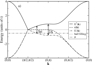
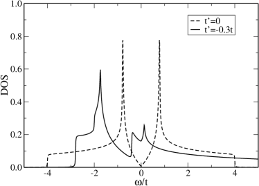
where the momentum sum is over the entire Brillouin zone, and this quantity does not depend on the chemical potential as it can be absorbed into the frequency. First, consider the case where . The upper, , and lower, , bands are shown in Fig. 1a for , illustrating that the gap is maximum at and closes at . For this band structure, at each value of momentum there are two branches, one for the upper and one for the lower antiferromagnetic Brillouin zone. This allows for vertical transitions with zero momentum transfer to be induced by the photon field from the lower to the upper band (interband transitions). Indicating schematically a Fermi level on the band structure diagram in Fig. 1a, such a transition from the Fermi level at in the lower band (hole doping) to the upper band, by an energy equal to , is shown. The significance of this result is that, in the absence of other mechanisms for absorption, such as impurity- or boson-assisted scattering, the minimum energy for an optical transition at finite frequency is . This becomes the cutoff of the interband optical signal at low frequencies as will be seen from our full calculations. The corresponding density of states for this bandstructure is shown in Fig. 2 as the dashed line, which is the conventional one for a d-wave order parameter. It has zero states at . For this case of , an analytical expression is available for the density of states in the continuum limit: , where is the complete Elliptic integral of the first kind and is the density of states at the Fermi level in the state without the pseudogap.
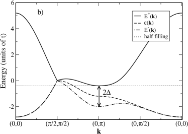
With nonzero, the bands and the density of states are modified. For small (), the band structure is similar to the one at with the lower band narrower and the upper band wider. If, on the other hand, is big (), the bands overlap, as shown in Fig. 1b for and the density of states is finite everywhere within the extended band.
IV Optical conductivity
We consider now the real part of the optical conductivity . In the long wavelength limit () the current operator in momentum space is:
| (10) | |||||
where the are the boson Matsubara frequencies. Within linear response theory, the optical conductivity is obtained from the current-current correlation function as , where is a Cartesian coordinate, . On the imaginary axis, is given in the bubble approximation in terms of the Matsubara Green’s functions by the following equation:
| (11) | |||||
When the Green’s function, given by Eq. (7), is expressed in terms of the spectral functions , the real part of the optical conductivity takes the form:
| (12) | |||||
where the Fermi function is given as and . If we do not include disorder in the system, we can express the conductivity as , where indicates the intraband conductivity or Drude weight and , the interband conductivity. Replacing the by their expressions in (II), we obtain for the weight of the intraband conductivity :
| (13) | |||||
and for the interband conductivity for :
| (14) | |||||
Concentrating first on the intraband conductivity given by Eq. (13), if we take both and the continuum limit, we can extract analytical information. For , Eq. (13) reduces to:
| (15) |
where
| (16) |
which can be further reduced in the continuum limit, after integration over energy, to:
| (17) |
where we have made the angular dependence of explicit in Eq. (17). Using the result that in two dimensions , where is the Fermi velocity, and setting to 1, Eq. (17) can be finally stated in terms of Elliptic functions as follows:
where is the Elliptic integral of the second kind. In the limit of small and relative to , one can find that:
| (19) |
For and , the Drude weight is zero, as expected from the density of states. As the temperature increases, spectral weight is transferred to the Drude, and likewise for finite .
Next, we return to the case of the interband conductivity. Setting in (14), the factor with the hyperbolic functions may be moved outside the momentum sum:
| (20) |
where we have defined:
| (21) |
It is now possible to obtain an analytical expression for in the continuum limit:
| (22) |
which can also be written in terms of Elliptic functions:
For small , and for , it is equal to . Thus the interband contribution to the conductivity varies as at low frequency, with inclusion of the thermal factors, and as at large , with a singularity expected at .
The function , which multiplies in Eq. (20), is a universal function that shows the dependence of the interband conductivity on temperature and chemical potential. Taking the limit of zero temperature, it becomes a step function ,i.e., zero, if and one, otherwise. At finite temperature, this step function becomes smeared. The fact that the interband conductivity starts abruptly at is an important feature of the DDW modelnayak . This feature does not arise, for example, in the case of the d-wave superconductor order parameterschachi , rather it is peculiar to the DDW model because the unconventional density wave gap opens up at the antiferromagnetic Brillouin zone boundary, while the d-wave superconductor order parameter opens up at the Fermi level.
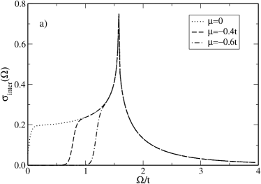
The interband conductivity for different values of the chemical potential is shown in Fig. 3 for a fixed value of the pseudogap, , and temperature, . Note that all figures for the conductivity are in arbitrary units. Fig. 3a has been calculated using the continuum limit given by Eq. (20) and Eq. (IV), and Fig. 3b using Eq. (14) with a lattice size . The main difference between the continuum limit and the discrete sum is that the singularity around is reduced for the calculation performed by summing over the full Brillouin zone. Because varies as when , the slope is set by , which becomes very steep when is small, as seen in Fig. 3 (dotted curve). On the other hand when is finite and , as we have already noted, the thermal factor in Eq. (20) provides a lower cutoff at , which is smeared in Fig. 3 due to finite temperature.
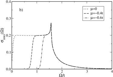
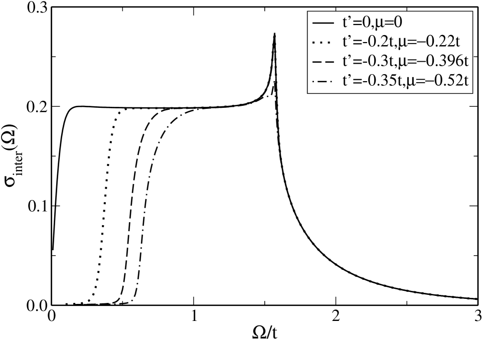
Next, considering the effect of on the interband conductivity, we return to Eq. (14). The expression in Eq. (14) depends on only through the hyperbolic cosine where the imperfect nesting dispersion adds directly onto the chemical potential. Hence, the non-nesting term will alter the lower cutoff on the interband conductivity. Indeed, numerical calculation shows that the cutoff, previously at , is shifted to lower frequency. The for different values of is shown in Fig. 4, which is to be compared with frame (b) of Fig. 3. In all cases, we have taken half filling, maintaining the doping fixed. The doping was defined, for temperature , by:
| (24) |
where is the density of states of Eq. (9), shown in Fig. 2, which is normalized to one state over the entire Brillouin zone. The shape of the interband region is not much affected by the value of , but the cutoff at low energy is now shifted down from , as discussed above. The surprising fact, that the shape of the interband contribution to the conductivity is not strongly affected by , may be understood by referring to Fig. 1. On comparison of frames (a) and (b), the essential feature is that both bands shift at any value of by the same amount , without significant change in the shape, which therefore does not affect the relative energy for vertical transitions.
We now turn to the total spectral weight, which has been discussed extensively as a key to understanding the mechanism of superconductivity.molegraaf ; bontemps ; benfatto Having obtained expressions for inter- and intraband conductivities, it is straightforward to evaluate the different contributions to the total spectral weight, and , and determine how they evolve with the various parameters of the model.
Integrating expression (14) with respect to , the interband spectral weight is given by:
| (25) |
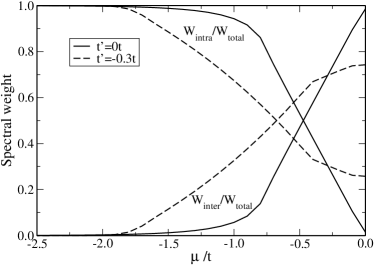
Thus, adding Eq. (25) to Eq. (13) (the intraband spectral weight), we obtain for total spectral weight . In Fig. 5, it is shown that the missing spectral weight, in the energy range from in the interband conductivity, is transferred to the Drude weight as increases. The solid curve applies to the case , which corresponds to the dashed line in Fig. 2 for the electronic density of states. For , all the optical spectral weight is in the interband contribution since at , in this case, and there can be no intraband conductivity as a result. As is increased the intraband part increases rapidly and nearly linearly as does versus of Fig. 2 in this range. As approaches in value the growth in becomes much less rapid and eventually saturates to being the total spectral weight. Thus, there is a transfer of spectral weight from the interband region to intraband when the doping is increased. While the results in Fig. 5 are based on the lattice sum expressions for and , the results just described can be understood simply from Eq. (15) in the continuum limit. At , becomes a delta function and the integral in Eq. (15) becomes equal to . This Elliptic function which describes the dependence of the intraband spectral weight on agrees remarkably well with the corresponding solid curve of Fig. 5. Next we consider the case for . The dashed curves in Fig. 5 apply to the case , which corresponds to the solid curve in Fig. 2 where we see that there is now a finite density of states even at and hence the intraband contribution starts from a finite value of approximately of the total weight. Because of the particular band structure involved, the intraband contribution first remains relatively flat until about , which is the value of the chemical potential at half filling for the particular parameters used here, and . Beyond , there is a linear behaviour similar to the one found for , although with a different slope, which finally saturates to where all the spectral weight is intraband.
In Fig. 6, we show results for (dashed), (dot-dashed) and (solid) as a function of the DDW gap in units of . In these calculations, and the doping was kept fixed at . Remarkably, the total spectral weight is only decreased from its value by about 6% at . As increases, the amount in the intraband component (which contains all the weight for ) gradually decreases, however, it is still about twice the amount of that in the interband at the largest value of considered.
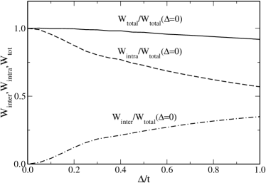
To conclude, we wish to emphasize that our most important results for the total spectral weight are: 1) there is a transfer in the spectral weight from the interband conductivity at low frequencies, , to the Drude weight at , and 2) even though a pseudogap has opened, the total spectral weight is changed only by a few percent at fixed doping in the cases we have studied.
Other aspects of the total spectral weight were considered recently by Benfatto et al.benfatto in relation to the temperature dependence of the total spectral weight and its relevance to the experimental results by Molegraaf et al.molegraaf , who found a very small decrease of with increasing temperature. Benfatto et al.’s work also examined the effect of different choice of current operators. Aristov and Zeyheraristov have also briefly commented on the spectral weight issue with respect to temperature variation. A feature of a recent work of Benfatto et al.benfatto2 is the examination of the role of ward identities and vertex corrections on the temperature dependence of the optical sum rule, where they find that the total spectral weight increases with decreasing temperature. While there is some difference between their total spectral weight and ours, upon comparison with the frequency-dependent optical conductivity, we find very little difference between our calculation and the one shown in their paper. They are virtually the same, with only a small quantitative difference at high frequency, and all the features discussed here remain intact. This indicates that these corrections, while important for the total spectral weight, may be neglected, as is common, for calculations of the frequency-dependent optical conductivity. Their work, done concurrently, is complementary to ours in that they examine primarily the issue of total spectral weight and we emphasize the details of frequency-dependent conductivity. Our aim in this work is to determine how the total spectral weight is distributed in the optical conductivity and where it transfers to upon the opening of the pseudogap.
V Electronic Raman scattering
Now that we understand the crucial role of the chemical potential in the optical conductivity (indicating the frequency above which the interband response is different from zero), we examine its effects on the Raman response. The Raman response has the advantage that different regions of the Brillouin zone may be selected via the choices of incoming and outgoing photon polarizations. In contrast, the optical conductivity is an average over all the Fermi surface. Hence, Raman experiments are relevant for unconventional density waves since they can provide information on the symmetry of the order parameter.
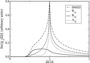
In the point group of the square lattice, we have three different channels:, , and . The channel projects out the antinodal region of the Fermi surface, the , the nodal region, and the is a weighted average over the entire Brillouin zone. In evaluating the Raman response for these different channels, we will discuss the continuum limit for simplicity.
The real part of the optical conductivity multiplied by frequency, i.e. , is related to the imaginary part of the Raman susceptibilityshastry , , in the case where the in the conductivity is replaced by , where is the Raman vertex for a particular channel. In the absence of impurities, the Drude part of the Raman signal is zero and the interband part turns out to be:
where stands for the three different channels mentioned above: , and , and we have defined:
| (26) |
The expressions for the unrenormalized Raman vertices in the continuum limit are:
| (27) | |||||
| (28) | |||||
| (29) |
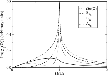
and we have absorbed additional constant factors in the and ’s which are arbitrary. The integrals in Eq. (V) can be written in terms of Elliptic integrals which have the same form as for a d-wave superconductor.dwayne The result is shown in Fig. 7 for and in Fig. 8 for . To better illustrate the role of the chemical potential in providing a lower frequency cutoff on the Raman signal, we have used . This is certainly not realistic. In fact, in the tight-binding approximation, the signal in is proportional to instead of ,t and as a consequence we expect that the signal will be much smaller than the other ones. In the low frequency regime, the (dotted) and the (solid) signals are proportional to , while (dashed) is proportional to . For comparison we have also included our results for (dash-dotted curve) based on Fig. 3a.
The Raman signal has recently been studied by Zeyher and Grecogreco within the model, with particular attention paid to the renormalization of the Raman vertices and to the role of superconductivity. Here, we are only interested in the mean field prediction for the region of the phase diagram where the DDW order prevails.
From Fig. 8 we conclude that the effect of the cutoff is easily seen in the and the signals, but less so for the channel, which is already quite small in magnitude at small . This is because the symmetry probes the antinodal quasiparticles where the pseudogap is largest.
VI Scattering
We now turn to the problem of scattering by impurities and inelastic scattering. We study only the optical conductivity since the results can be easily extrapolated to the Raman response. To include quasiparticle scattering, we replace the delta functions inside the spectral functions in Eq. (II), with Lorentzians of the form:
| (30) |
where and is the self-energy due to impurities or coupling to inelastic scattering. These are inserted in the optical conductivity given by Eq. (12).
We study two cases, the scattering rate equal to a constant: , and the scattering rate of the marginal Fermi liquid: where and are constants.
VI.1
If , then . The effect of adding a constant scattering rate is that the interband contribution can no longer be separated from the Drude contribution. Still, these two contributions can be clearly discerned in the real part of the conductivity for a large range of parameters.
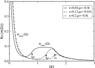
For the numerical calculations of the optical conductivity given by Eq. (12), we have used a lattice size of 300x300 for the Brillouin zone sum. The evolution with doping of the is shown in Fig. 9. In this figure, we can clearly see the redistribution of the spectral weight between the Drude contribution and the interband contribution when the doping is varied. In all these curves, solid for , dashed for and dash-dotted for x=0.2, the lower edge of the interband region is at as indicated by arrows with some smearing due to temperature and impurity scattering. This edge moves upwards with increasing doping. There is little change however in the upper edge of the band at approximately . For the dash-dotted curve, the interband region is almost completely gone and has been transfered to the Drude peak which has increased optical strength as compared to the solid curve. The effect of varying the impurity parameter is very straighforward and, therefore, not shown. As is increased the Drude component at low frequency is broadened in width and the peak drops, likewise the interband contribution is further smeared out and reduced in height.
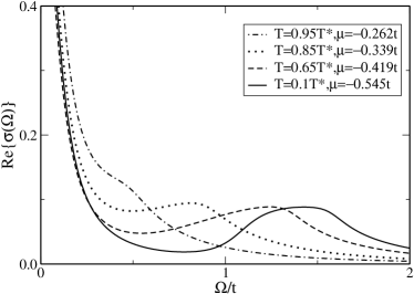
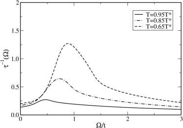
We now turn to the question of how varies with temperature for fixed doping. For this calculation we have used a fitted dependence of the gap with temperaturebenfatto : , where we have chosen . As the temperature is increased, the gap seen as the upper edge of the interband transitions moves to lower frequencies because the pseudogap closes. Secondly, the depression between low frequencies and is filled in with increasing temperature. More importantly, the Drude weight increases with increasing temperature because of the collapse of the interband region. The DC conductivity displays a typical semiconducting behaviour with resistivity decreasing with increasing temperature. However, in these calculations we have kept the scattering rate constant. In any realistic case, the inelastic scattering will increase with . This can be modelled by a temperature dependent scattering rate which increases with temperature, therefore reducing the DC conductivity, and as a result there can be a change of its behaviour from semiconducting to metallic. Such inelastic scattering would modify the result of Fig. 10. It would broaden the Drude peak relatively to what is seen and fill in the region between the intraband and interband contributions even more, obscuring the cutoff.
Experimentally, the spectral weight distribution at low frequency and its temperature dependence has been studied in reference bontemps . For their underdoped sample, the spectral weight in the pseudogap region, does not move to lower frequencies with increasing temperature as is predicted in DDW theory, but rather it has the opposite behaviour; the spectral weight at low frequencies moves to the Drude with decreasing temperature.puchkov ; bontemps This behaviour could only be obtained in the DDW model with strong inelastic scattering.
Next, we calculate another important quantity that is obtained in optical experiments, namely the optical scattering rate. For this, we use the extended Drude model:tanner-timusk ; puchkov
| (31) |
where we have calculated numerically the by Kramers-Kronig relations, and for the plasma frequency we have used that derived from the Drude weight in the case of . The result is shown in Fig. 11. The most striking feature in this figure is a peak which arises from the interband contribution. This is an important result since, in principle, it can be verified experimentally. We note that as the temperature increases, the size of the peak decreases in magnitude and shifts to lower energy before disappearing completely at the pseudogap temperature . Also the position of the peak in the scattering rate of Eq. (31) is not at the same position as the peak in the real part of the conductivity. It is lower. In particular for the solid curve in Fig. 11, which is the highest temperature shown, the peak falls below while the corresponding structure in the real part of the conductivity in Fig. 10 is nearer , although in that case it cannot be characterized simply as a peak. Later, we will comment on the origin of these shifts, between the scattering rate and the optical conductivity, of the interband structure. A second feature to be noted in Fig. 11 is that the scattering rates at are considerably larger than twice the value of the impurity scattering rate that we have used. This feature will also be addressed at the end of this section. Finally, as discussed before, if the impurity parameter is increased, the conductivity is broadened and the effect on the peak seen in the scattering rate is for it to be broadened and reduced. Recently a peak in in the region of to has been observed in the cobaltatestimuskCo . This peak reduces and eventually vanishes with increasing temperature. There appears to be a corresponding peak in the conductivity, as well, at higher frequency (400 to 6000 cm-1), not unlike what we find in our model.
VI.2 Inelastic scattering
To present a more realistic comparison with experiments, we should include the inelastic scattering. It is important to check whether or not the strong feature found above, in the optical scattering rate, will be washed out by the inelastic scattering. We can do this using the self-energy of the marginal Fermi liquidmfl in our spectral functions . This phenomenological model assumes that the excited charge carriers interact with a wide, flat spectrum of excitations over , where is a high energy cutoff of the spectrum. This model was introduced to explain the observed linear behaviour in the scattering rate measured in the optical conductivity, as well as in the resistivity, and in the Raman cross-section.varma ; tanner-timusk
The marginal Fermi liquid ansatz is:tanner-timusk ; mfl
| (32) |
where is a dimensionless coupling constant.
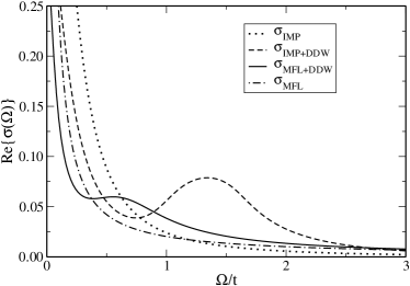
Results based on the MFL self-energy are shown in Fig. 12, where they are also compared with previous results for impurities alone (i.e., a constant scattering rate). The dotted line is for and the dash-dotted curve is for plus the MFL contribution to the self-energy. On comparing these two curves, both calculated at temperature , we note that considerable optical spectral weight is lost at small in the dash-dotted curve, as compared to the dotted Drude curve. There is a crossing at slightly above 1 and for the MFL there is a long tail in the mid-infrared region of the optical spectrum, extending to high and staying well above the Drude curve. These tails are an essential feature of the conductivity in the cuprates, an indication of a strong electron-boson inelastic contribution (Holstein band). The depletion of the optical weight at small reflects the fact that the quasiparticle spectral weight in the MFL, , varies as at small and therefore vanishes logarithmically at the Fermi surface. The other two curves in Fig. 12 include a DDW. The dashed curve is based on a constant quasiparticle scattering rate of while the solid curve is for . The interband contribution manifests itself as a broad peak centered around , in the dashed curve, which is also reasonably well separated from the Drude contribution centered around . As the impurity scattering is increased, the region between the interband and the intraband fills in, and the interband peak broadens and is reduced in height (not shown). In a sense, the MFL result (black curve) can be understood as a case where impurity scattering effectively increases with increasing frequency. This has the outcome of spreading the interband spectral weight over a much larger frequency range reducing the prominence of the peak seen in the dashed curve and shifting it to lower energy. Because of this shift, it is not possible to accurately determine the size of the pseudogap from the effective position of the interband transitions in the real part of the conductivity. Nevertheless, a peak still remains in the MFL case, although now it is not so well separated from the intraband contribution at low energies and the cutoff is no longer visible.
We also note from Eq. (12), that for the DC conductivity at zero temperature, the electron spectral functions are all evaluated at zero frequency. In this case, only the impurity self-energy remains, since in Eq. (32), therefore, both the impurity and the marginal Fermi liquid models will have the same DC value because we have chosen the same and plasma frequency in both cases. However, for finite temperature, the marginal Fermi liquid DC conductivity will be reduced because of the inelastic scattering, a feature not present in the impurity case. When the DDW gap is included, spectral weight is transferred to the interband processes. In both cases of impurity only and impurity plus MFL, this transfer of spectral weight is about for the parameters chosen, namely and . This is consistent with the solid curves in Fig. 5 which cross at this value of the chemical potential for . For the impurity case the value of the DC conductivity is reduced to of its original value while for the marginal Fermi liquid the percentage is .
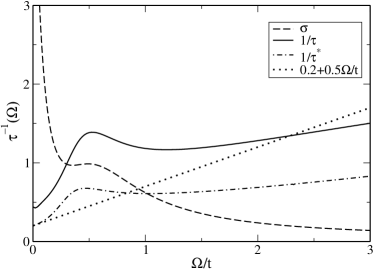
In Fig. 13, we show our results for the optical scattering rate obtained from the marginal Fermi conductivity of Fig. 12. What is shown as the solid curve is the usual of Eq. (31). It is this quantity that is used in the experimental literature. However, it is useful to define a new scattering rate denoted by which is related to by a simple multiplicative constant. For , what is used for forming the righthand side of Eq. (31) is the value of the DC conductivity divided by , rather than . For the impurity case without the DDW, this would give , as would also be the case for the pure MFL at . At , an inelastic contribution to the scattering would also need to be added to . For the case shown here, where , this is about a 10% correction. As we have seen, when the DDW is present, considerable spectral weight is transferred from the intraband to the interband absorption, and so the Drude centered about is strongly depleted, and the DC conductivity is correspondingly reduced. This means that is about one half the value of for the case considered here when the DDW is present. An important feature of is that as , it agrees exactly with the residual scattering rate with two modifications. First, when quasiparticle scattering is present, the interband contribution can make a contribution to the DC conductivity, and second, at finite temperature in the MFL, there can also be a small increase in the DC scattering due to the inelastic scattering. Both these effects can modify somewhat the of the . Returning now to Fig. 11, we can understand why, in the lower temperature run, the DC limit of is more than twice the value of . It reduces with increasing temperature but even for the solid curve at , it is still above . Returning to the solid curve of Fig. 13, we note that its DC value is also above mainly due to the depletion of the intraband contribution. At higher frequencies, it shows the interband peak slightly below and then takes on a quasilinear behaviour as expected of the pure MFL, but with a slope which is considerably reduced over the input scattering rate, shown as the dotted curve. The reduction in slope can be traced to the presence of the interband transitions as will be made clear in the following.
We now turn to the shift in the interband structure toward lower frequency seen in the scattering rate of Fig. 13 when compared to the structure in the conductivity of Fig. 12. This also holds for Fig. 11 when compared to Fig. 10. Some understanding of this can be obtained from the study of a simplified model. For convenience, we use a simplified form for the marginal Fermi liquid conductivity:tanner-timusk
| (33) |
Note that for the conductivity, it is which enters as the damping rate. The constant impurity scattering rate is twice its quasiparticle counterpart, but the MFL piece remains unaltered. Eq. (33) is a reasonably useful approximation to the more accurate calculation that would arise from implementing the exact form for the normal state conductivity:frank
| (34) |
with the marginal Fermi liquid self-energy given in Eq. (32). Adding to Eq. (33) a form based on a displaced Lorentzian oscillator in the dielectric function of energy , which is used to model the interband contribution:ziman
| (35) |
we form the optical scattering rate defined in Eq. (31) for the combined system with one change. Instead of using the complete plasma frequency coming from interband and intraband combined, we use only the intraband contribution. This is done to define . We use Eq. (33) and Eq. (35) to model as well as possible the solid curve (MFL+DDW) in Fig. 12. The result is shown in Fig. 13 as the dashed line. The parameters used are , , , and . With these parameters we can calculate the scattering rate for our model. It is given by the dash-dotted curve which can be compared with the dotted straight line equal to . These quantities agree at as expected. It is to be noted that this graph provides a good qualitative confirmation of the complete numerical results of Fig. 13 (solid curve). We note that differs from of formula Eq. (31) mainly by a constant numerical factor. We also note that the peak in the scattering rate has shifted downward as compared with its position in the conductivity. This is clearly due to the particular combination of real and imaginary part of the conductivity defined in Eq. (31). The reduced slope of the quasi-linear behaviour of the dash-dotted curve at large when compared with the pure MFL slope is reproduced in our model (solid curve). It can now be seen that it has its origin in the fact that an interband contribution is present and is not due to an alteration of the MFL representation of the remaining intraband contribution (with the lorentzian term set to zero, we recover the straight dotted line as expected). We can conclude from this analysis that, to good approximation, the complete conductivity can be nicely modelled as a superposition of a MFL component of reduced spectral weight, but otherwise unaltered, plus an interband component given approximately by Eq. (35). This reproduces the full numerical calculation reasonably well, however, the original pseudogap value and cutoff could never be inferred from fitting the experimental data to this model.
In principle, the formation of a DDW will also lead to changes in the self-energy of the charge carriers. For example in the DDW model the electronic density of states acquires additional energy dependence as seen in Fig. 2 which, in turn alters the quasiparticle scattering.hirschfeld ; kimcarbotte Here, we have modelled this scattering either with a constant elastic scattering rate or, to be more realistic, by a marginal Fermi liquid (MFL) contribution. This contribution to the inelastic scattering is directly responsible for the quasilinear dependence, in frequency , of the optical scattering rate, seen in Fig. 13 at beyond the interband contribution. This quasilinear dependence is a hallmark of the cuprates and is central to the MFL phenomenology which was introduced to correlate a large number of the normal state properties of the high oxides, which are anomalous. Unfortunately, there is no generally accepted underlying microscopic frameworkmicro to the marginal Fermi liquid ansatz, which could be employed to introduced the necessary modifications to the self-energy that result from the DDW formation. Such considerations go beyond the scope of the present study.
The effects of energy dependence in the electronic density of states on the self-energy and on the conductivity have recently been studiedmeirong for elastic impurity scattering and are well understood. For example, a depression in below its constant background value around the Fermi energy, leads directly to a corresponding reduction in the optical scattering rate in this same frequency region. In a non-self-consistent approach, the constant quasiparticle scattering rate of the flat case, is simply multiplied by to lowest order. In our case, this would be the of the DDW as shown in Fig. 2. This would correspondingly reduce the scattering rate of Fig. 13 at small . However, it was found in referencemeirong that such a procedure overestimates the effect of on the quasiparticle as well as on the optical scattering rate. In a self-consistent approach, the impurities and, even more importantly, the inelastic scattering of the MFL smear out the structures in which are due to the opening of the DDW gap. Nevertheless, a reduction of below the value seen in Fig 13 is expected for frequencies below the gap and would be associated with self-energy corrections.
Finally, we discuss the issue of comparison with experiment. This model predicts the appearance of an interband contribution in the pseudogap phase and an accompanying peak in the optical scattering rate. This interband contribution should have a feature at lower energy corresponding to a lower cutoff set by and a higher cutoff of about . The lower feature should shift to higher energy with increased doping, however, from experiment the gap decreases with doping and hence the upper edge in the conductivity should decrease with increased doping. This has not been seen in experiments on the high cuprates. Examples of optical experiments examining the underdoped state of various cuprates are given in Refs. puchkov ; puchkovprl ; takenaka for YBCO, Bi2212, and LSCO materials. There is no evidence for an interband feature with energy scales as described here and the optical scattering ratepuchkov does not show a peak. The most up-to-date review on optical conductivity experiments in high cupratesbasov does not give further evidence that could support this model. Indeed the DDW model has been controversial in its applicability to experiments in the cuprates. Some criticisms have involved the variance of the model with regard to photoemissionzxshen and tunnelingkimcar2 , but some of these issues have been possibly rectified by further calculationchakraphoto ; greco2 . Here we find that the experimental evidence from optical conductivity, at this time, does not support the DDW model for the cuprates. However, this model may find application in other systems in the future.
VII Conclusions
We have calculated the optical conductivity and the Raman response for a DDW system. There is a cutoff at low frequencies in the interband response for both the optical conductivity and the Raman response. This cutoff is at if there is no imperfect nesting term in the dispersion relation. The imperfect nesting adds directly to the chemical potential and shifts the cutoff to lower frequency but does not eliminate it. Including scattering makes the cutoff harder to discern.
As the chemical potential is changed we find a readjustment of the spectral weight between the inter- and intraband conductivities. That part of the interband contribution, ranging from frequencies zero to , is transferred at zero temperature to the Drude weight as the chemical potential is increased with increasing doping. However, contrary to a first expectation there is little loss in the total spectral weight with the opening of the pseudogap. This result agrees with experiments.bontemps
As mentioned above, the cutoff also appears in the electronic Raman scattering. The best channels to observe the cutoff at are and . The channel projects out the antinodal region where the gap is biggest, and the low intensity of the Raman scattering at small , where it goes like , may make the cutoff difficult to see.
The behaviour with temperature of the optical conductivity has two characteristics: 1) the expected shift of the feature to lower frequencies, for a mean field theory with order parameter vanishing at , and 2) the transfer of spectral weight from interband to intraband as the interband contribution collapses. There is also a filling of the depression between low frequencies and .
An important result of this paper is that there is a peak in the real part of the optical conductivity in the region that comes from the interband conductivity with for . This peak is robust against different dispersion relations including second-nearest-neighbours. It is reduced by the impurity scattering and by the inelastic scattering, which can also shift it. It is washed out with increasing temperature vanishing completely at the pseudogap critical temperature. Similar structure is found in the optical scattering rate, but it is shifted relative to that in the optical conductivity. With strong inelastic scattering, as may be found in the MFL model, the cutoff and features become more difficult to determine directly. To the best of our knowledge, this interband structure has not yet been identified in experiments on cuprates.
Acknowledgements.
EJN acknowledges funding from NSERC and the Government of Ontario (Premier’s Research Excellence Award), and the University of Guelph. JPC acknowledges support from NSERC and the CIAR. We thank L. Benfatto, W. Kim, and D. Basov for helpful discussions.References
- (1) T. Timusk and B. Statt, Rep. Prog. Phys. 62, 61 (1999) and references therein.
- (2) H. Ding, T. Yokoya, J. C. Campuzano, T. Takahashi, M. Randeria, M.R. Norman, T. Mochiku, K. Kadowaki, and J. Giapintzakis, Nature (London) 382, 51 (1996).
- (3) A.G. Loeser, Z.-X. Shen, D.S. Dessau, D.S. Marshall, C.H. Park, P. Fournier, and A. Kapitulnik, Science 273, 325 (1996).
- (4) Ch. Renner, B. Revaz, J.-Y. Genoud, K. Kadowaki, and O. Fischer, Phys. Rev. Lett. 80, 149 (1998).
- (5) V. J. Emery and S.A. Kivelson, Nature (London) 374, 134 (1995).
- (6) E. Carlson, V.J. Emery, S.A. Kivelson, and D. Orgad in The Physics of Conventional and Unconventional Superconductors edited by K.H. Bennemann and J.B. Ketterson (Springer-Verlag, New York, 2004).
- (7) Q.J. Chen, I. Kosztin, B. Jankó, and K. Levin, Phys. Rev. Lett. 81, 4708 (1998).
- (8) S. Chakravarty, R.B. Laughlin, D.K. Morr, and C. Nayak, Phys. Rev. B 63, 094503 (2001).
- (9) S. Chakravarty, H.-Y. Kee, and C. Nayak, Int. J. Mod. Phys. B 15, 2901 (2001).
- (10) Q. -H. Wang, J.H. Han, and D -H. Lee, Phys. Rev. Lett. 87, 077004 (2001).
- (11) J. -X. Zhu,W. Kim, C. S. Ting, and J. P. Carbotte, Phys. Rev. Lett. 87, 197001 (2001).
- (12) X. Yang and C. Nayak, Phys. Rev. B 65, 064523 (2002).
- (13) B. Dóra, A. Virosztek, and K. Maki, Phys. Rev. B 65, 155119 (2002). K. Maki, B. Dóra, M. Kartsovnik, A. Virosztek,B. Korin-Hamzic,and M. Basletic, Phys. Rev. Lett. 90, 256402 (2003).
- (14) B. Dóra, K. Maki, and A. Virosztek, Mod. Phys. Lett. B. 18, 327 (2004).
- (15) S. Chakravarty, C. Nayak, and S. Tewari Phys. Rev. B 68, 100504 (2003).
- (16) I. Schürrer, E. Schachinger and J.P. Carbotte, Physica C 303, 287 (1998).
- (17) H.J.A. Molegraaf, C. Presura, D. van der Marel, P.H. Kes, and M. Li, Science 295 2239 (2002).
- (18) A. F. Santander-Syro, R.P.S.M. Lobo, N. Bontemps, Z. Konstantinovic, Z. Li,and H. Raffy, Phys. Rev. Lett. 88 97005 (2002).
- (19) L. Benfatto, S.G. Sharapov and H. Beck, Eur. Phys. J. 39, 469 (2004).
- (20) D.N. Aristov and R. Zeyher, cond-mat/0406419
- (21) L. Benfatto, S.G. Sharapov, N. Andrenacci, and H. Beck, Phys. Rev. B 71, 104511 (2005).
- (22) B.S. Shastry and B.I. Shraiman, Int.J.Mod.Phys. B 5 365 (1991). D. Branch and J.P. Carbotte, Jour. Supercon. 13 535 (2000).
- (23) D. Branch, MSc Thesis McMaster University, (1995).
- (24) Strictly speaking, is a universal function only for . However, since we already know that the effect of is to shift the cutoff at , we still use this universal function in the continuum limit.
- (25) R. Zeyher and A. Greco, Phys. Rev. Lett. 89, 177004 (2002).
- (26) A.V. Puchkov, D.N. Basov, and T. Timusk, J. Phys.: Condens. Matter 8, 10049 (1996).
- (27) D.B. Tanner and T. Timusk, in The Physical Properties of High Temperature Superconductors III,D.M. Ginsberg, Ed. (World Scientific, Singapore, 1992),pp. 363-469.
- (28) J. Hwang, J. Yang, T. Timusk, and F.C. Chou, cond-mat/0405200.
- (29) C. M. Varma, P. B. Littlewood, S. Schmitt-Rink, E. Abrahams and A. E. Ruckenstein, Phys. Rev. Lett. 63, 1996 (1989).
- (30) C. M. Varma, Phys. Rev. B 55, 14554 (1997).
- (31) F. Marsiglio, T. Startseva, and J.P. Carbotte, Phys. Lett. A 245, 172 (1998).
- (32) See for instance, J.M. Ziman, Principles of the Theory of Solids (Cambridge University Press, 1965).
- (33) P.J. Hirschfeld, P. Wölfle, and D. Einzel, Phys. Rev. B 37, 83 (1988); P.J. Hirschfeld, W.O. Putikka, and D.J. Scalapino, Phys. Rev. B 50 10250 (1994).
- (34) W. Kim and J.P. Carbotte, Phys. Rev. B 66, 033104 (2002).
- (35) Theories that reproduce the marginal Fermi liquid behaviour for a specific region of the phase diagram of the cuprates are the nested Fermi liquid, A. Virosztek and J. Ruvalds, Phys. Rev. B 42,4064 (1990) and the so-called Van Hove scenario, J. González, F. Guinea, and M.A.H. Vozmediano, Nucl. Phys. B 485, 694 (1997).
- (36) M.-R. Li and J.P. Carbotte, Phys. Rev. B 60, 155114 (2002).
- (37) A.V. Puchkov, P. Fournier, T. Timusk, and N.N. Kolesnikov, Phys. Rev. Lett. 77, 1853 (1996).
- (38) K. Takenaka, J. Nohara, R. Shiozaki, and S. Sugai, Phys. Rev. B 68, 134501 (2003).
- (39) D.N. Basov and T. Timusk, Rev. Mod. Phys., in press.
- (40) A. Damascelli, Z. Hussain, and Z-X. Shen, Rev. Mod. Phys. 75, 473 (2003).
- (41) W. Kim, J.-X. Zhu, J.P. Carbotte, and C.S. Ting, Phys. Rev. B 65, 064502 (2002).
- (42) A. Greco and R. Zeyher, Phys. Rev. B 70, 024518 (2004).