[
Highly polarized injection luminescence in forward-biased ferromagnetic-semiconductor junctions at low spin polarization of current
Abstract
We consider electron tunneling from a nonmagnetic -type semiconductor (-S) into a ferromagnet (FM) through a very thin forward-biased Schottky barrier resulting in efficient extraction of electron spin from a thin -S layer near FM-S interface at low spin polarization of the current. We show that this effect can be used for an efficient polarization radiation source in a heterostructure where the accumulated spin polarized electrons are injected from -S and recombine with holes in a quantum well. The radiation polarization depends on a bias voltage applied to the FM-S junction.
]
The desire of building scaleable devices using an electron spin created a new field of spintronics [1]. Some spintronics effects, like a giant magnetoresistance of multilayers and tunnel structures [2, 3, 4], already found many applications. Of particular interest is an injection of spin-polarized electrons into nonmagnetic semiconductors (NS) because of a long spin-relaxation time [1, 5] and a prospect of using this phenomenon for ultrafast spintronic devices and possibly quantum computers [1]. Different ferromagnet-semiconductor-ferromagnet (FM-S-FM) structures have been suggested including those where electron spin is affected by an applied electric field [6], an external magnetic field [7], or a magnetic field produced by a nanowire current [8]. All these devices are controllable spin valves where one of FM-S junctions acts as a spin source and another one as a spin filter. The latter efficiently transmits electrons with a certain spin projection and reflects electrons with the opposite spin. The spin polarization of photoexcited electrons in NS, some effects and devices due to spin reflection off a ferromagnet have been studied in Refs. [9]. Spin injection from magnetic semiconductor in NS has been reported in Refs. [10]. Spin accumulation and extraction from NS was predicted in Ref. [11] in forward-biased p-n junctions containing magnetic semiconductors and observed recently in MnAs/GaAs junction [12]. Spin injection from FM into NS was demonstrated in Refs. [13, 14]. Optimal conditions of the spin injection from FM into NS have been discussed in Refs. [7, 8, 15, 16, 17, 18, 19, 20].
The injection of spin polarized electrons from FM into NS is determined by a current in a reverse-biased FM-S Schottky junction. Such a current is negligible due to a high Schottky barrier usually forming at FM-S interface [21]. Therefore, an ultrathin heavily doped interfacial semiconductor layer (doped layer) is used to thin down the barrier considerably and increase the current [14, 7, 8, 18, 19]. The conditions for the most efficient spin injection in a reverse-biased FM-S junction have been studied in Refs. [18, 7, 8, 19]. In forward-biased FM-S Schottky junctions, thermionic emission current reaches large values at a bias voltage close to , where is the barrier height and the elementary charge. Realization of the spin injection due to such a current is problematic since electrons in FM with an energy are weakly spin polarized ( is the Fermi level in FM). Recently we considered a forward-biased FM-S junction with a doped layer and showed [20] that tunnelling of electrons from a NS into a FM through the doped layer can result in efficient extraction of electrons with a certain spin and accumulation of electrons with the opposite spin in NS near the interface.
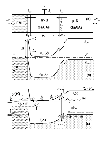
In this paper we consider a structure containing a FM-S junction with the doped layer and a double heterostructure where -region made from narrower gap semiconductor, Fig. 1. We show that the following effects can be realized in the structure when both FM-S junction and the heterostructure are biased in forward direction and electrons are injected from -semiconductor region into FM and -region. Due to a spin selection property of FM-S junction [20], spin polarized electrons appear in -region with a spatial extent near the FM-S interface, where is the spin diffusion length in NS. When thickness of the -region is smaller than the spin polarized electron from the -region and holes from -region are injected and accumulated in a thin narrow-gap -region (quantum well) where they recombine and emit polarized photons. The degree of the polarization depends on the bias voltage of FM-S junction, , since different correspond to electron states in FM with different polarization [see curve for in Fig. 1(c)]. Thus, the structure allows to study the dependence and find the optimal bias such that the polarization of spin and radiation is maximal.
Let us now consider these effects in greater detail. The spatial distribution of a spin density in a semiconductor is determined by the continuity equation [15, 17]
| (1) |
where is the current of electrons with spin , , and are the density and the spin-relaxation time of electrons in the -semiconductor region. In Ref. [20] we showed that a tunneling current in a forward-biased FM-S junction with the doped layer is
| (2) | |||||
| (3) |
the current of electrons with spin near the interface, and , given by
| (4) |
and the distribution of is characterized by a length , where and are the diffusion and the drift lengths of electron spin in the NS, respectively [15, 17]; and are the diffusion constant and the mobility of electrons, and is the electric field in S. We have introduced , the tunneling transparency of the modified FM-S junction [7, 8, 20], the spin polarization of nonequilibrium electrons near interface that defines the degree of spin extraction from S, , the spin factor , and the effective spin polarization characterizing spin selection of the modified FM-S junction [7, 8, 20]
| (5) |
Here is the velocity of electron with spin in the FM, the tunneling “velocity” in the NS, and are the thermal velocity and the effective mass of electrons in NS, the voltage drop across the FM-S interface, is height of potential barrier at FM-S interface, , the bottom of conduction band in -region in equilibrium, Fig. 1(b).
The conditions for maximal polarization are obtained as follows. When the thickness of -region is we can assume that and . In this case, integrating Eq. (1) over the volume of the -semiconductor region (with area and thickness ), we obtain
| (6) |
Here ; and are the electron currents with spin flowing into the -region from FM and the -region, respectively; is the spin current out of the -region in a contact, Fig. 1(a). The current is determined by injection of electrons with from the -region into the p-region, equal to , where is the total current in the junction. The current of metal contact is not spin polarized, hence , where is the total current in FM-S junction. Thus, we can rewrite (6) with the use of Eq. (4) as
| (7) |
The current in FM-S junction approaches a maximal value at rather small bias, since at (2). When and we get from Eq. (7)
The way to maximize is evident from Eq.(5) showing that it depends on and , i.e. it corresponds to an electron energy , Fig.1. Therefore, depends on bias voltage of FM-S junction and one may be able to maximize a spin extraction and accumulation by adjusting . The maximal can be achieved for the process of electron tunneling through the -doped layer when the bottom of conduction band in a semiconductor is close to a peak in the density of states of minority carriers in the elemental ferromagnet, Fig. 1(c, curve g). Indeed, the density of states for minority d-electrons in Fe, Co, and Ni at ( eV) is much larger than that of the majority electrons, , and electrons, [22]. Therefore, due to the polarization may be close to 100%.
Polarization of injection luminescence is determined by recombination of injected spin polarized electrons and holes inside the -region of the double heterostructure of thickness , Fig. 1. The injection current of electrons with into the -region is
| (8) |
where is the density of electrons with spin , , ( is the time of spin relaxation (recombination) of electrons in the -region. We notice that in III-V compound semiconductors, including GaAs and GaAlAs, there are light holes with spin and heavy holes with spin . Recombination of light and heavy holes with electrons having spin results in radiation of photons with an opposite polarization (. To exclude this undesirable effect, the thickness and the hole potential well in the narrow-gap -region, Fig. 1, should be such that the light holes, unlike the heavy holes, cannot be localized inside the well. In this case we can neglect the light holes, assuming that the concentration of heavy holes in the well is much larger than that of the light holes. Then, the rate of polarized radiation recombination is and the polarization of radiation is . Since we find from (8) that , so that . Thus, the radiation polarization can approach maximum at large current when . The latter condition can be met at high concentration when the time of radiation recombination . For example, in GaAs s at cm-3 [23] and can be larger than [1, 5].
We emphasize that spin polarization of current near a forward-biased FM-S junction is very small. Indeed, according to Ref. [20] at as Thus, polarization of the recombination radiation would be high, , while the spin polarization of current in FM-S junction is low.
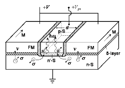
Practical structures may have various layouts, with one example shown in Fig. 2. It is clear that the distribution of in such a two-dimensional structure is characterized by the length in the direction where the electrical field can be strong, and by the diffusion length in the () plane where the field is weak. Therefore, the spin density near FM and junctions will be close to when the size of -region is . Thus, the above derivation and results for one-dimensional structure, Fig. 1, are also valid for more complex geometry shown in Fig. 2. The predicted effect should also exist for a reverse-biased FM-S junction where the radiation polarization can approach
REFERENCES
- [1] S. A. Wolf et al., Science 294, 1488 (2001); Semiconductor Spintronics and Quantum Computation, edited by D. D. Awschalom et al. (Springer, Berlin, 2002).
- [2] J. S. Moodera et al., Phys. Rev. Lett. 74, 3273 (1995); M. Baibich et al., ibid. 61, 2472 (1988); A. E. Berkowitz et al., ibid. 68, 3745 (1992).
- [3] J. C. Slonczewski, Phys. Rev. B 39, 6995 (1989).
- [4] A. M. Bratkovsky, Phys. Rev. B56, 2344 (1997).
- [5] A. G. Aronov et al., Sov. Phys. JETF 57, 680 (1983) [Zh. Eksp. Teor. Fiz. 84, 1170 (1983)]; J. M. Kikkawa et al., Science 277, 1284 (1997); D. Hagele et al., Appl. Phys. Lett. 73, 1580 (1998); J. M. Kikkawa and D. D. Awschalom, Nature 397, 139 (1999); I. Malajovich et al., Nature 411, 770 (2001).
- [6] S. Datta and B. Das, Appl. Phys. Lett. 56, 665 (1990); S. Gardelis et al., Phys. Rev. B 60, 7764 (1999).
- [7] A. M. Bratkovsky and V. V. Osipov, Phys. Rev. Lett. 92, 098302 (2004).
- [8] V. V. Osipov and A. M. Bratkovsky, Appl. Phys. Lett. 84, 2118 (2004).
- [9] C. Ciuti et al., Appl. Phys. Lett. 81, 4781 (2002); R. J. Epstein et al., Phys. Rev. B 65, 121202 (2002); C. Ciuti et al., Phys. Rev. Lett. 89, 156601 (2002).
- [10] R. M. Stroud et al., Phys. Rev. Lett. 89, 166602 (2002); M. Tanaka and Y. Higo, ibid. 87, 026602 (2001); Y. Ohno et al., Nature 402, 790 (1999); R. Fiederling et al., ibid. 402, 787 (1999).
- [11] I. Zutic et al., Phys. Rev. Lett. 88, 066603 (2002).
- [12] J. Stephens et al., cond-mat/0404244 (2004).
- [13] J. Zhu et al., Phys. Rev. Lett. 87, 016601 (2001); P.R. Hammar et al., ibid. 83, 203 (1999); W.Y. Lee et al., J. Appl. Phys. 85, 6682 (1999); R. Meservey and P.M. Tedrow, Phys. Rep. 238, 173 (1994).
- [14] A. T. Hanbicki et al., Appl. Phys. Lett. 82, 4092 (2003); A. T. Hanbicki et al., ibid. 80, 1240 (2002).
- [15] A. G. Aronov and G. E. Pikus, Sov. Phys. Semicond., 10, 698 (1976).
- [16] M. Johnson and R.H. Silsbee, Phys. Rev. B 35, 4959 (1987); P.C. van Son et al., Phys. Rev. Lett. 58, 2271 (1987); G. Schmidt et al., Phys. Rev. B62, R4790 (2000); E.I. Rashba, ibid. 62, R16267 (2000).
- [17] M.E. Flatte and J.M. Byers, Phys. Rev. Lett. 84, 4220 (2000); Z. G. Yu and M. E. Flatte, Phys. Rev. B 66, R201202 (2002); Z. G. Yu and M. E. Flatte, ibid. 66, 235302 (2002).
- [18] J. D. Albrecht and D. L. Smith, ibid. 66, 113303 (2002).
- [19] V.V. Osipov and A.M. Bratkovsky, cond-mat/0307030.
- [20] A.M. Bratkovsky and V.V. Osipov, cond-mat/0307656.
- [21] S.M. Sze, Physics of Semiconductor Devices (Wiley, New York, 1981); W. Mönch, Semiconductor Surfaces and Interfaces (Springer, Berlin, 1995).
- [22] I.I. Mazin, Phys. Rev. Lett. 83, 1427 (1999); V. L. Moruzzi et al., Calculated Electronic Properties of Metals (Pergamon, New York, 1978).
- [23] A.P. Levanyuk and V.V. Osipov, Sov. Phys. Usp. 24, 3 (1981) [Usp. Fiz. Nauk 133, 427 (1981)].